國 立 交 通 大 學
電子工程學系 電子研究所碩士班
碩 士 論 文
考量閘極可靠度之
晶片上靜電放電防護電路設計
Design of On-Chip ESD Protection
Circuits with Consideration of
Gate-Oxide Reliability
研究生 : 陳 穩 義
指導教授 : 柯 明 道 教授
中華民國九十四年四月
考量閘極可靠度之晶片上靜電放電防護電路設計
Design of On-Chip ESD Protection Circuits
with Consideration of Gate-Oxide Reliability
研 究 生:陳穩義 Student:Wen-Yi Chen
指導教授:柯明道 教授 Advisor:Ming-Dou Ker
國 立 交 通 大 學
電子工程學系 電子研究所碩士班
碩 士 論 文
A ThesisSubmitted to Institute of Electronics
College of Electrical Engineering and Computer Science National Chiao-Tung University
in partial Fulfillment of the Requirements for the Degree of
Master in
Electronic Engineering April 2004
Hsinchu, Taiwan, Republic of China
考量閘極可靠度之晶片上靜電放電防護電路設計
學生:
陳穩義
指導教授:
柯明道
教授
國立交通大學
電子工程學系
電子研究所碩士班
摘
要
本論文旨在討論由於製程進步與電路結構改變,所造的靜電放電防護設計的問題,並進 一步提出解決方案。設計宗旨為不需額外光罩與製程步驟,僅利用電路上的設計來提升靜電 放電防護能力。並可將本論文所提出的設計應用於不同製程上,不會侷限於某些特定製程才 能達到效果,因此可廣泛地應用在不同晶片設計上。 第一個設計為利用一閘極電壓鉗制電路,將 N 型金氧半導體的閘極電壓,在靜電放電 發生的情況下,有效鉗制在一電位,避免過高的閘極電壓吸引過高的靜電放電電流,燒毀元 件的氧化層,藉以有效克服閘極過度耦合效應的問題。本設計並可簡單調整靜電放電時的閘 極耦合電壓大小,以應用於具有不同閘極厚度的製程設計。本設計實際驗證於0.35-μm 互補 式金氧半導體製程。於此驗證中,具有閘極電壓鉗制電路設計的 N 型金氧半導體,其機器 放電模式的靜電放電防護能力獲得30%的改善。 第二個設計為一電源線間的靜電放電防護電路。本設計的特點在於可操作在3.3-V 的高 電源電壓下,但只使用1-V/2.5-V 的低壓元件,且不會有閘極可靠度的問題。本應用特別適 用於高/低壓共容輸出/入介面的設計上,並搭配內部電路的設計,無需使用較厚閘極氧化層 的3.3-V 元件而使用較薄閘極氧化層的 2.5-V 元件,使電路可應用在較高的操作頻率,縮短 產品的市場導入時程,並可避免製程限制的窘境。本設計驗證於具 1-V/2.5-V 邏輯元件的 0.13-μm 互補式金氧半導體製程。實驗結果證明本設計在正常工作電壓下具有極小的漏電電 流,對靜電放電事件具有極快的反應時間,並具有優異的靜電放電防護能力。Design of On-Chip ESD Protection Circuits
with Consideration of Gate-Oxide Reliability
Student: Wen-Yi Chen Advisor: Ming-Dou Ker
Department of Electronics Engineering and Institute of Electronics
National Chiao-Tung University
A
BSTRACTThe aim of this thesis is to propose solutions of ESD protection problems under the consideration of gate-oxide reliability. Objectives of the proposed designs are to achieve the desired ESD protection capabilities in circuit technique without modifying process steps or increasing mask layers. Therefore, the proposed designs are suitable to different CMOS processes and therefore can be widely applied to different circuit designs.
The first proposal is a gate-voltage-limited circuit that can clamp the coupled gate voltage of an gate-coupled NMOS device during ESD transition. The over-coupled gate voltage of an NMOS device draws over-huge ESD current in the channel region and burns out the gate oxide of the NMOS device. The gate-voltage-limited circuit can therefore prevent the gate-coupled devices from the over-gate-driven effect. This design was fabricated and verified in a 0.35-μm CMOS process. Experimental results show that a gate-coupled NMOS with the proposed gate-voltage-limited circuit can have a 30% improvement on its MM ESD protection level compared to a gate-coupled NMOS without the proposed circuit.
The second proposal is a power-rail ESD clamp circuit. The specialty of this proposed design is that it is designed with only 1-V and 2.5-V low voltage devices to be operated under the 3.3-V high power-supply voltage without the gate oxide reliability issue. This proposed design can collocate with mixed-voltage I/O designs to achieve a higher circuit operation frequency. This
proposed design was fabricated and verified in a 0.13-μm 1-V/2.5-V CMOS process. Experimental results show that the proposed design has extremely small standby leakage current under the normal circuit operating condition. This design also shows fast turn-on speed under ESD stresses and high ESD protection robustness.
Contents of this thesis have already been published on two international conferences and submitted to two international journals.
誌
謝
碩士班能順利畢業,第一個要感謝的是我的指導教授 柯明道博士,從大學部的專題到 研究所,一路上的諄諄教誨以及辛勤督導,還有盡可能在研究資源上的幫助,讓我在碩士學 位的路途上,得到許多的成長。 柯老師教導給我的不只在知識上,還有對自己應負責任的 堅持,未來工作上應有的正面態度…等。回想現在的自己與大學剛畢業的我,從 柯老師身 上學到的身教以及言教,實在太多太多。 其次,我要特別感謝已從本實驗室畢業的 徐國鈞博士,以及目前在聯詠科技的 張智毅 先生。他們在我求學的路上對我所請教的問題不厭其煩地替我解說,引領我在短時間內進入 碩士班的領域。並且三不五時被我拉去吃飯聊天,在生活的態度,以及人生路途的抉擇上讓 我獲益良多。在這段路途上沒有二位,我也不能走得如此順遂,在此對兩位獻上特別的感謝。 另外,我要感謝在工研院以及華邦電子的學長、朋友們,有他們的支持與陪伴,讓我在 學校以外還有另一塊生活圈,也有另一個知識的來源,也讓了解到學校以外的業界是怎麼樣 的情形。工研院的莊哲豪學長,陳子平學長,林昆賢學長,彭政傑學長,世宏,項彬;以及 在華邦電子的林奕成先生,曾仁洲先生…等。實驗室的學長朋友們也伴我良多,許勝福,陳 榮昇,陳世倫,張瑋仁,鄧至剛,徐新智學長們,還有同學吳偉琳,陪我一起走過碩士班的 路程,一起熬夜做實驗,在這裡一併獻上對你(妳)們的感激。 最後我要感謝的是自己的父母親 陳世霖先生與 林清珠女士。父母對我在生活上以及經 濟上的支持,是讓我無後故之憂唸完碩士班的最大支柱。對父母該感謝的太多,不是三言兩 語可用文字寫盡,在這裡誠心地對我偉大的父母親致上感謝。以及哥哥陳瑞宗,來自家人的 關照還是最溫暖的來源。還有我的女朋友陳瑩柳小姐,從大學到研究所畢業,總是在背後替 我打點瑣事,也在背後鼓勵我渡過每一個低潮,盡力給我協助。 其他該感謝的人還有很多,對一路上曾經幫助過我的各位,在此一併獻上感激之情。 陳穩義 94年3月Content
ABSTRACT (CHINESE)………..……….…i
ABSTRACT (ENGLISH)………..………...…………ii
ACKNOWLEDGEMENT………...iv
CONTENTS………...………v
TABLE CAPTIONS………...……viii
FIGURE CAPTIONS………...…..ix
Chapter 1 Introduction………...1
1.1 M
OTIVATION………..………...….1
1.2 T
HESISO
RGANIZATION……….………..2
Chapter 2 Introduction to ESD and the Effects of
Process Migration to ESD Protection Designs………4
2.1 G
ENERALI
NTRODUCTION TOESD……….4
2.1.1 Human Body Model (HBM)……….…...4
2.1.2 Machine Model (MM)………5
2.1.3 Charged Device Model (CDM)………..5
2.2 ESD
T
ESTM
ETHODS………..6
2.2.1 ESD Test on I/O Pins……….…...6
2.2.2 Pin to Pin ESD Test………6
2.2.3 VDD-to-VSS ESD Test………7
2.5 T
RIGGERINGT
ECHNIQUES TOESD
P
ROTECTIOND
EVICES………10
2.5.1 Gate-driven Technique……….…...10
2.5.2 Substrate-triggered Technique………11
2.6 E
FFECTS OF THEP
ROCESSM
IGRATION TOESD
P
ROTECTIOND
ESIGNS….…11
2.6.1 The Over-Gate-driven Effect……….…...12
2.6.2 High Voltage Tolerant ESD Protection Design……….…...12
Chapter 3 Circuit Solution to Overcome the Over-Gate-Driven
Effect on ESD Protection Circuits in Deep-Submicron
CMOS Processes………18
3.1 I
NTRODUCTION………18
3.2 T
HEO
VER-G
ATE-D
RIVENE
FFECT………19
3.2.1 Non-uniform Turn-on Behavior……….…...19
3.2.2 Gate-coupled Technique……….….…………20
3.2.3 Over-Gate-Driven Effect……….….…………21
3.3 C
IRCUITS
OLUTION TOO
VERCOME THEO
VER-G
ATE-D
RIVENE
FFECT…...…23
3.3.1 Design Concept……….…...23
3.3.2 Gate Voltage Monitor Circuit……….…...23
3.4 E
XPERIMENTALR
ESULTS………...…25
3.4.1 Clamping by NMOS String……….….…………25
3.4.2 Clamping by Diode String……….….…………29
3.5 C
ONCLUSION………...…30
Chapter 4 Design on Power-Rail ESD Clamp Circuit for 3.3-V I/O
Interface By Using Only 1-V/2.5-V Low-Voltage Devices
in a 130-nm CMOS Process………44
4.1 I
NTRODUCTION………44
4.2 ESD P
ROTECTIONS
CHEME FOR1-V/3.3-V
M
IXED-V
OLTAGEI/O
I
NTERFACE………45
4.2.1 ESD Protection Scheme……….….…………45
4.2.2 Review on High Voltage Tolerant Power-Rail ESD Clamp Circuit…46
4.3 N
OVELP
OWER-R
AILESD
C
LAMPC
IRCUIT FORH
IGH-V
OLTAGEA
PPLICATIONS………48
4.3.1 Circuit Operation Under Normal Power-on Transition….…………49
4.3.2 Circuit Operation Under ESD Transition……….…………49
4.4 E
XPERIMENTALR
ESULTS………51
4.4.1 Standby Leakage Current………51
4.4.2 Turn-on Verification………52
4.4.3 ESD Robustness………54
4.4.4 Failure Analysis………55
4.4.5 Silicon Controlled Rectifier (SCR) as ESD Clamp Device…………55
4.5 C
ONCLUSION………56
Chapter 5 Conclusion and Future Work……….68
5.1 C
ONCLUSION………68
5.2 F
UTUREW
ORK………69
References……….70
Table Captions
Table 4.1
Device Dimensions of the ESD Protection Circuit in this Work………58Table 4.2
Leakage Current of Prior Arts and the New Proposed Power-Rail ESD Clamp Circuit……….58Table 4.3
ESD Robustness of STNMOS Devices with or without the New Proposed ESD Detection Circuit……….58Figure Captions
Fig. 2-1 The equivalent circuit of the human body model ESD event……….13 Fig. 2-2 Definition of the HBM pulse decay time (td). ………13 Fig. 2-3 The equivalent circuit of the machine model ESD event………14 Fig. 2-4 The current waveform of a 400-V MM ESD stress discharging through a short wire…14 Fig. 2-5 Comparison on waveforms of a 2-kV HBM ESD stress, 200-V MM ESD stress,
and a 1-kV CDM ESD tress………15 Fig. 2-6 (a) PS-mode, (b) NS-mode, (c) PD-mode, and (d) ND-mode, ESD test on I/O pins…15 Fig. 2-7 (a) Positive mode, (b) Negative-mode, pin-to-pin ESD test………16 Fig. 2-8 (a) Positive mode, (b) Negative-mode, VDD-to-VSS ESD test………16 Fig. 2-9 The ESD current discharging paths (path 1 and path 2) during the pin-to-pin
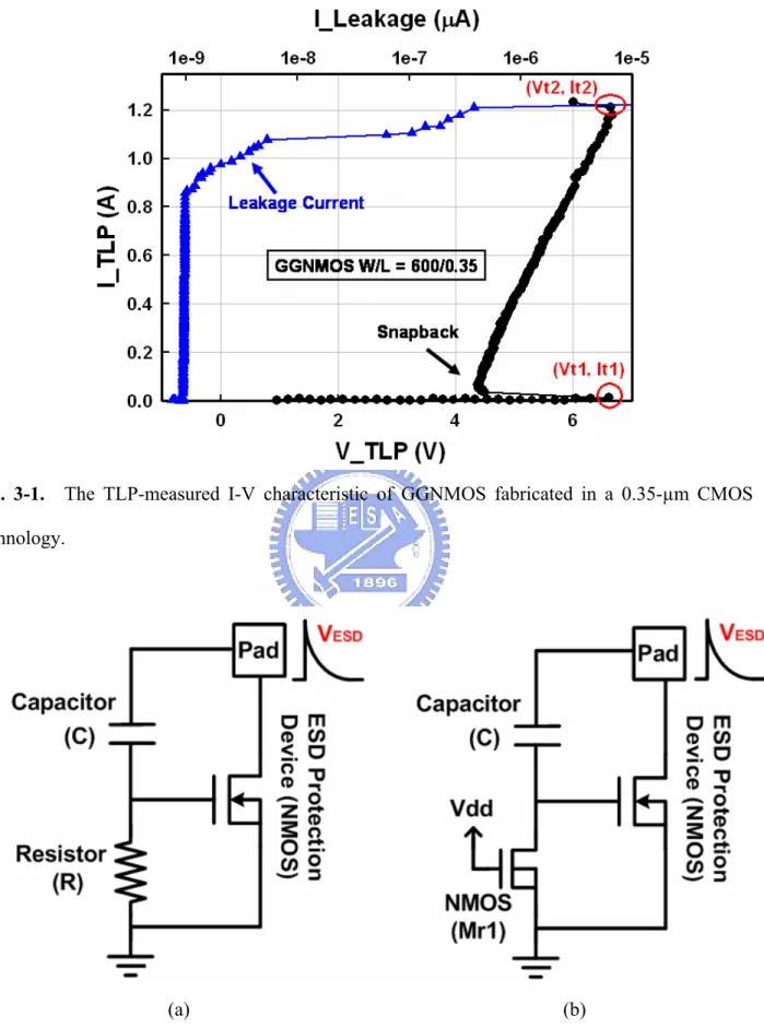
ESD stress condition………17 Fig. 2-10 Cross sectional view of a SCR device………17 Fig. 3-1 The TLP-measured I-V characteristic of GGNMOS
fabricated in a 0.35-µm CMOS Technology………31 Fig. 3-2 Two traditional circuit design methods to carry out the gate-coupled technique and
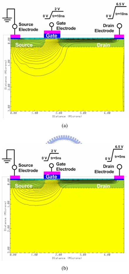
to solve the non-uniform turn-on behavior in the ESD protection NMOS………31 Fig. 3-3 The simulated current flow lines of NMOS with a bipolar trigger voltage of 5.7 V.
Voltages applied to drain and gate electrodes are respectively ramped to 6.5 V and 2 V with simultaneous rise time of (a) 10 ns, and (b) 5 ns………..…32 Fig. 3-4 MM ESD levels of NMOS (W/L= 600 μm/0.35 μm) under different gate voltages…33 Fig. 3-5 A novel circuit design concept which can overcome the over-gate-driven effect for
ESD protection circuits with gate-coupled or gate-driven technique………33 Fig. 3-6 The gate voltage monitor circuit added on-chip can monitor Vg of GCNMOS during
Fig. 3-7 The measured Vdet voltages when (a) 10-V, and (b) 15-V, voltage pulse with a rise time of 10 ns is applied to the GCNMOS without gate-voltage-limited circuit………..35 Fig. 3-8 Id-Vg curve of the gate voltage monitor circuit in a 0.35-μm CMOS process…………36 Fig. 3-9 The measured Vdet voltages when (a) 10-V, and (b) 20-V, voltage pulse with a rise
time of 10 ns is applied to the GCNMOS with two stacked NMOS devices in the gate-voltage-limited circuit. Each stacked NMOS has a device dimension (W/L)
of 50 μm/0.35 μm………37 Fig. 3-10 The measured Vdet voltages when the 20-V voltage pulse with a rise time of 10 ns
is applied to GCNMOS with (a) three, and (b) five, stacked NMOS devices in the gate-voltage-limited circuit. Each stacked NMOS has a device dimension (W/L) of
50 μm/0.35 μm………...………..…………38
Fig. 3-11 The measured Vdet voltages when 20-V voltage pulses with rise time of 10 ns are applied to GCNMOS with two different gate-voltage-limited circuits. One consists of three stacked NMOS devices with each device dimension (W/L) of 20 μm/0.35 μm, the other consists of three stacked NMOS devices with each device dimension
of 50 μm/0.35 μm………39 Fig. 3-12 MM ESD levels of the GCNMOS with different numbers or different device
dimensions of stacked NMOS devices in the gate-voltage-limited circuit……..………39 Fig. 3-13 SEM image of the GCNMOS with two stacked NMOS devices in the
gate-voltage-limited circuit after 550-V MM ESD stress. Each stacked NMOS
has device dimension (W/L) of 70 μm/0.35 μm………40 Fig. 3-14 SEM image of (a) the GCNMOS with five stacked NMOS devices in the
gate-voltage-limited circuit after 600-V MM ESD stress. Each stacked NMOS has device dimension (W/L) of 20 μm/0.35 μm. (b) The enlarged image of its ESD
Fig. 3-15 SEM image of (a) the GCNMOS with five stacked NMOS devices in the gate-voltage-limited circuit after 650-V MM ESD stress. Each stacked NMOS has device dimension (W/L) of 70 μm/0.35 μm. (b) The enlarged image of its
ESD failure location………42 Fig. 3-16 MM ESD levels of the GCNMOS with different numbers or different device
dimensions of stacked diodes in the gate-voltage-limited circuit………43 Fig. 4-1 ESD protection schemes for mixed-voltage I/O interfaces (a) with, and (b) without, the
dummy supply line VESD………59
Fig. 4-2 The cross-sectional view of a forward-biased stacked-diode string to show the
parasitic p-n-p BJTs and its leakage current path. ………60 Fig. 4-3 The new proposed power-rail ESD clamp circuit with only 1-V and 2.5-V devices
for operating under high-voltage VDD_h of 3.3V………60 Fig. 4-4 Hspice-simulated voltages on nodes of the ESD detection circuit under normal
power-on transition with a rise time of 1ms………61 Fig. 4-5 Hspice-simulated voltages on nodes of the ESD detection circuit and the current
of Mp2 under 0-to-7V ESD-like transition………61 Fig. 4-6 The snapback I-V characteristic curve of a stand-alone STNMOS device………62 Fig. 4-7 The leakage currents of STNMOS with or without the ESD detection circuit under
different temperatures………62 Fig. 4-8 The clamped voltage waveforms by STNMOS with or without the ESD detection
circuit under the voltage pulse stress with the pulse height of 20V and the rise time of 10ns……….………63 Fig. 4-9 The measured substrate-triggered current generated by the ESD detection circuit
under 0-to-7V voltage pulse with a rise time of 10ns on the VDD_h pin………63 Fig. 4-10 TLP-measured I-V curves of STNMOS with ESD detection circuit under
Fig. 4-11 The (a) OBIRCH, and (b) SEM, images of a 400μm/0.3μm STNMOS with
ESD detection circuit after 325-V MM ESD stress………65 Fig. 4-12 SEM image of (a) a stand-alone 400μm/0.3μm STNMOS after 175-V MM ESD
stress. (b) The enlarged image of its ESD failure location………66 Fig. 4-13 SEM image of a stand-alone 400μm/0.3μm STNMOS
after 1.5-kV HBM ESD stress………67 Fig. 4-14 TLP-measured I-V characteristics of both SCR with and without ESD detection
Chapter 1
Introduction
━━━━━━━━━━━━━━━━━━━━━━━━━━━━━━━━━━━━━━━
1.1 M
OTIVATIONESD protection design has already been granted as one of the major challenges for deep-submicron CMOS technologies [1]. To reduce the power consumption and to increase the operating speed of IC chips, both the gate oxide thickness and the operating voltage of MOS devices keep scaling down. The progress is positive to the performance of IC chips but negative to the ESD protection because the on-chip devices are more and more fragile. Some problems are therefore comes into being with the progress of CMOS processes.
The gate-driven (or gate-coupled) technique has been widely used on ESD protection designs to shorten the turn-on time and to improve the turn-on uniformity of ESD protection devices for a long time [2]–[7]. However, with the constant shrinkage on gate-oxide thickness of MOSFET devices in deep-submicron CMOS processes, the gate-coupled technique has been found to adversely affect the ESD robustness of NMOS devices [8]-[10]. It has been also found that the thinner the gate oxide is, the severer degraded is the ESD robustness of NMOS devices [9]. In deep-submicron CMOS processes, the over-gate-driven effect is a problem in urgent. A new approach to overcoming the over-gate-driven-effect through the circuit structure is proposed in this thesis [11]. The proposed design is portable to different process technologies without modifying mask layers or process steps. With the proposed design, the gate-driven or gate-coupled technique can be devised more easily and properly.
In modern IC chips, though the power supply voltage of internal circuits keeps lowering to reduce the power consumption and the heat dissipation, their input/output interfaces are still
operated at higher voltage levels to cooperate with the peripheral components. For such mixed-voltage applications, special design through circuit structure or process modification is needed to avoid the gate-oxide reliability issue. Though the process technology can provide devices with different gate-oxide thickness to meet the requirement, it is not cost-effective and will lower the production yield in manufacturing. Devices with thicker gate-oxide also have worse device characteristics such as the inferior device driving capability, impeding the high speed system performance. A better solution to both overall system performance and cost is to propose a high-voltage tolerant circuit that can be operated under high power-supply voltage but is fabricated with only low-voltage devices. In this thesis, a substrate-triggered power-rail ESD protection circuit with only 1-V/2.5-V devices to sustain 3.3-V power supply voltage is proposed [12]. This substrate-triggered ESD clamp circuit is specially designed without suffering the gate-oxide reliability issue under the 3.3-V power supply voltage. The proposed ESD clamp circuit is fabricated and verified in a 130-nm 1-V/2.5-V CMOS process and shows extremely low standby leakage current, which is only 1/100 compared to the prior arts.
1.2 T
HESISO
RGANIZATIONThe chapter 2 of this thesis introduces ESD events, ESD test methods, and general ESD protection techniques. The motivation of bringing up proposed designs, the gate-voltage limited circuit to overcome the over-gate-driven effect (in chapter 3), and the power-rail ESD protection circuit for 1-V/3.3-V mixed-voltage I/O interfaces (in chapter 4), is also concisely introduced in this chapter.
The chapter 3 of this thesis discusses the benefits and the problems of the gate-driven technique. This chapter includes methods to overcome the over-gate-driven effect, its design concept, measurement setup, and experimental results. This design is fabricated and verified in a 0.35-μm CMOS process. The usefulness of the gate-voltage limited circuit on protecting
gate-driven devices against the over-gate-driven effect is proven through the measured ESD protection levels and the failure analyses.
In the chapter 4, a power-rail ESD clamp circuit for 1-V/3.3-V I/O interfaces is proposed. The proposed power-rail ESD clamp circuit is designed with only 1-V/2.5-V low-voltage devices but can be safely operated under 1-V/3-3-V mixed-voltage environment without the gate-oxide reliability issue. The proposed clamp circuit has an on-chip ESD detection circuit that can provide substrate-triggered current to substantially improve the turn-on efficiency of ESD protection devices. This protection design is successfully verified in a 130-nm 1-V/2.5-V CMOS process. Experimental results of the proposed clamp circuit show high ESD protection capability with very low leakage current, which is one of the main concerns for portable designs. As a result, the proposed power-rail ESD clamp circuit is an excellent ESD solution especially to the portable electronic devices with mixed-voltage I/O interfaces.
Chapter 2
Introduction to ESD and the Effects of
Process Migration to ESD Protection Designs
━━━━━━━━━━━━━━━━━━━━━━━━━━━━━━━━━━━━━━━
2.1
G
ENERALI
NTRODUCTION TOESD
ESD is a phenomenon caused by the discharging of electrostatic charges on IC pins. It can be arose from events such as a physical contact of a human body and an IC products, touch of manufacturing machines and wafers, or discharge of secondhand induced electrical field on an IC chips. Because ESD can be brought about by different origins, it can be classified to human-body model (HBM), machine-model (MM), and charged-device model (CDM) according to different discharging methods and sources of electrostatic charges.
2.1.1 Human-Body Model (HBM)
HBM is a typical ESD event arose from the contact of an electrified human body and an IC
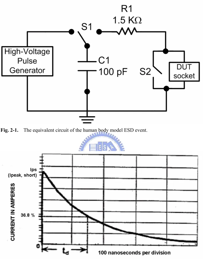
product. The ESD static charges are initially stored in the human body and then transfer into the IC when the human body touches the IC. The equivalent circuit for HBM ESD event is shown in Fig. 2-1 [13], where the 1.5-kΩ resistor and the 100-pF capacitor represent the equivalent parasitic resistor and capacitor of a human body. The DUT in Fig. 2-1 represents the device under test. The HBM circuit is designed to eliminate the weak protection designs and susceptible devices of the DUT. Fig. 2-2 shows the specifications of a HBM ESD waveform generated by the ESD HBM tester to a short wire [13]. Generally, commercial ICs are requested to pass 2-kV HBM ESD stress at least, which can generate ESD current with a peak value of ~1.3Amp and a rise time of ~10ns.
2.1.2 Machine Model (MM)
The equivalent circuit diagram of MM ESD event is shown in Fig. 2-3 [14], where there is no equivalent resistor on the equivalent discharging path because the MM ESD stress is to replicate the ESD event arose from the contact of a machine and a semiconductor device. Fig. 2-4 shows the waveform of a 400-V MM ESD pulse generated by the MM ESD tester [14]. A commercial IC product is generally required to pass at least 200-V MM ESD stress, which can generate an ESD current with a peak value of ~3.5Amp and a rise time of ~10ns. The MM ESD level of a semiconductor device is generally 8~12 times smaller than its HBM ESD level for the faster rise time and voltage resonance of a MM ESD pulse.
2.1.3 Charged-Device Model (CDM)
The CDM ESD event is caused by the discharging of electrostatic charges initially stored in the
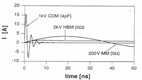
body of a floating IC. Most of the CDM charges are stored in the body (the p-substrate) of a CMOS IC at first. When one or more pins of this charged IC is touched by an external grounded object, charges in the p-substrate will be discharged from the IC inside to the grounded pin outside. There is no standard equivalent parasitic capacitor for the CDM ESD stress because different dimension of chips, different form and size of packages result in different values of the parasitic capacitor of IC chips. A commercial IC is generally requested to pass at least 1-kV CDM ESD stress, which can generate an ESD current with peak current value as high as ~15A within a rise time less than 200ps [15]. Fig. 2-5 compares the waveforms of a 2-kV HBM ESD stress, a 200-V MM ESD stress, and a 1-kV CDM ESD stress which has 4-pF equivalent capacitor of the device under test.
2.2
ESD
T
ESTM
ETHODSSince electrical charges in natural environment can be either positive or negative, ESD tests have positive and negative modes, too. Moreover, since ESD event can occur on input/output (I/O) pins, power pins, or between different I/O pins of an IC chip, ESD test methods have pin combinations as follows:
2.2.1 ESD Test on I/O Pins
For every I/O pin of an IC chip under the human-body model and the machine-mode ESD tests, there are four test modes as illustrated through Fig. 2-6(a) to 2-6(d) [16], [17]:
(1). PS mode
Positive ESD voltage applied to the tested I/O pin with VSS pins relatively grounded. VDD pins and all other pins are kept floating during the test, as shown in Fig. 2-6(a).
(2). NS mode
Negative ESD voltage applied to the tested I/O pin with VSS pins relatively grounded. VDD pins and all other pins are kept floating during the test Fig. 2-6(b).
(3). PD mode
Positive ESD voltage applied to the tested I/O pin with VDD pins relatively grounded. VSS pins and all other pins are kept floating during the test, Fig. 2-6(c).
(4). ND mode
Negative ESD voltage applied to the tested I/O pin with VDD pins relatively grounded. VSS pins and all other pins are kept floating during the test, Fig. 2-6(d).
2.2.2 Pin-to-Pin ESD Test
Besides the ESD test on I/O pins, ESD events can happen on one of the I/O pins with another I/O pin relatively grounded. If the two I/O pins are not correlated to each other in circuitry, ESD current will first be diverted from the stressed I/O pin to the VDD or VSS power line, and then be
discharged to the grounded I/O pin. Therefore, during the pin-to-pin ESD tests, power pins of the tested chip are kept floating. However, it could take a long testing period if every I/O pin of an IC chip is tested one by one. To shorten the testing period, positive or negative ESD voltage is applied on the tested I/O pin with all other I/O pins relatively grounded, as illustrated in Fig. 2-7(a) and Fig. 2-7(b).
2.2.3 ESD Test on Power Pins (VDD-to-VSS ESD Test)
The ESD test on power pins, or the VDD-to-VSS ESD stresses, simulate ESD events that happen between two power pins. A positive or a negative ESD voltage during the VDD-to-VSS ESD stress is applied to the VDD power pin of the device under test while the VSS power pin is relatively grounded, as shown in Fig. 2-8.
2.3
ESD
P
ROTECTIONN
ETWORKThe various ESD test methods suggest that ESD events can damage not only I/O circuits but also internal circuits, especially under the pin-to-pin and the VDD-to-VSS ESD stresses. These two ESD test modes often lead to some unexpected ESD current through the I/O ESD protection circuits and the power lines into the internal circuits and result in ESD damage on the internal circuits [18], [19]. Therefore, to effectively protect chips from the ESD damage, ESD protection designs are required on both I/O circuits and between the power lines. Fig. 2-9 illustrates the impact of the power-rail ESD clamp circuit to the discharging paths of ESD current (IESD) under the
specified pin-to-pin ESD stress. When a positive ESD voltage is applied to some input pin (I/P) with some output pin (O/P) grounded and the VDD and VSS pins floating, some ESD current will be diverted from the input pin to the floating VDD power line and then to the internal circuits (path 1), if the power-rail ESD protection circuit is not designed in Fig. 2-9. The ESD protection circuits at the I/O pins are often designed strong enough to discharge the huge ESD current, but the internal
circuits are easily damaged to cause unexpected damages on internal circuits. If an effective ESD clamp circuit is added between the VDD and VSS power lines, the ESD current can be discharged through the power-rail ESD clamp circuit (path 2) instead of the internal circuits (path 1). Therefore, the internal circuits can be safely protected against such unexpected ESD damage. Moreover, the power-rail ESD clamp circuit can also protect the whole chip against the VDD-to-VSS ESD testing mode. Thus, an effective power-rail ESD clamp circuit between the VDD and VSS power lines is necessary for the whole-chip ESD protection [19].
Therefore, a whole-chip ESD protection network should include not only ESD protection circuits at the I/O pins but also power-rail ESD clamp circuits. The whole-chip ESD protection network, appropriate ESD protection devices, and effective techniques to trigger the ESD protection devices are the keys for IC products to carry off high ESD robustness.
2.4
ESD
P
ROTECTIOND
EVICES INM
ODERNCMOS
IC
STo protect ICs from being damaged by ESD current, it is important to choose appropriate ESD protection device under different ESD protection networks and different system specifications. In modern CMOS ICs, ESD protection devices in common use include:
(1). P-N Junction Diode:
A diode device has low forward cut-in voltage (~ 0.6 V) and high reverse breakdown voltage, which can be higher than 10 V. Both forward diodes in series and a reverse diode can serve as the ESD protection circuit to protect internal circuits from being damaged by ESD current. When a reverse diode is used as an ESD protection device, its reverse breakdown voltage is required to be smaller than the gate oxide breakdown voltage of MOS devices so that ESD current can be discharged to ground through the reverse diode without damaging the gate oxide of internal circuits. A larger device dimension of the ESD protection diode is also required when it is operated
in reverse mode because the high reverse breakdown voltage generates huge heat to be dissipated during ESD stresses.
(2). MOS Device (NMOS or PMOS):
MOS devices are the most common ESD protection devices in CMOS ICs. The n+ drain junction, p-substrate and the n+ source junction of an NMOS device construct a parasitic n-p-n bipolar junction transistor. When the high ESD stress voltage occurs, the parasitic n–p-n bipolar junction transistor inherent in NMOS’s device structure can be turned-on to carry the huge ESD current and to clamp down the ESD voltage to protect gate oxide of internal circuits. As a result, the I-V characteristic curve of an NMOS device under ESD stresses often has the snapback phenomenon due to the turn on of the parasitic n-p-n bipolar.
The p+ drain junction, n-well substrate and p+ source junction of PMOS device form a parasitic p-n-p bipolar junction transistor inherent in its device structure. PMOS devices in CMOS ICs can therefore serve as an ESD protection device. However, the beta gain of p-n-p bipolar junction transistor in CMOS process is much smaller than that of n-p-n bipolar junction transistor; I-V characteristic curves of PMOS under ESD stresses have no, or weak, snapback phenomenon. (3). Field Oxide Device (FOD):
The field oxide device has similar device structure to that of NMOS device in CMOS process except the gate oxide of NMOS is replaced by the field oxide structure. The I-V characteristic curves of FOD under ESD stresses have larger turn-on resistance compared to that of NMOS because the depth of field oxide structure makes the ESD current discharging path of FOD longer than that of NMOS.
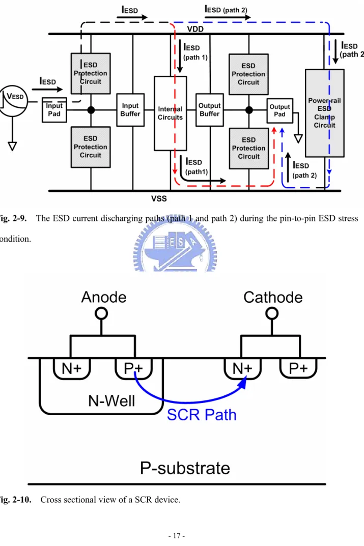
(4). Silicon Controlled Rectifier (SCR):
SCR device is a component with p-n-p-n structure, as shown in Fig. 2-10. A SCR device has a p-n-p and an n-p-n bipolar junction transistor with regenerative feedback to each other, so that SCR device can clamp the ESD voltage at a relatively low holding voltage (~1.2 V) compared to that of NMOS and FOD devices. Therefore, SCR device can achieve high ESD protection level
within small layout area due to its low holding voltage. However, a SCR device has drawbacks such as high turn-on voltage, low turn-on speed, and latch-up issue.
To sum up, different ESD protection devices have respective advantages and disadvantages. Therefore, it is important to pick the appropriate device as an ESD protection element according to different power-supply voltages, ESD protection networks, system specifications, and device characteristics.
2.5
T
RIGGERINGT
ECHNIQUES TOESD
P
ROTECTIOND
EVICESIn most applications, MOS devices are used as ESD protection elements in CMOS ICs. With the process scaling down, thickness of gate oxide of MOS devices in deep-submicron CMOS technologies keeps shrinking to achieve higher system operating frequency, lower power consumption and lower heat dissipation. As a result, the gate oxide breakdown voltages of MOS devices keep going down toward their junction breakdown voltages. Internal circuits protected by stand-alone ESD protection devices, which have no triggering techniques to increase their turn-on efficiencies, are therefore easily damaged under ESD stress. Moreover, it is also found that ESD levels of large-device-dimension NMOS devices are constrained by the non-uniform turn-on behavior [20]-[23], making it difficult for IC chips to have high ESD robustness. There are two popular measures that can be realized in circuitry to effectively increase the turn-on efficiency and uniformity of ESD protection devices: the gate-driven and the substrate-triggered techniques.
2.5.1 Gate-driven Technique
To prevent ESD protection devices from interacting with the signals in normal operation, the gate electrode of the ESD protection NMOS is grounded in most applications. This can also ensure that the NMOS has its minimum leakage under normal operation. However, a MOS device can be a more robustness ESD protection element if its gate is coupled high during ESD transition [2]-[7].
The gate-driven (or the gate-coupled) technique is to design a special ESD detection circuit that can drive the gate voltage of ESD protection NMOS high during ESD transition but keep the gate potential low to ensure the chip function during normal circuit operation. The gate-driven technique drives gate voltage of NMOS high to induce its channel current during ESD transition. The induced channel current can therefore help forward bias the base-emitter junction of parasitic n-p-n bipolar and increase its turn-on efficiency during ESD transition.
2.5.2 Substrate-Triggered Technique
The other method to improve the turn-on efficiency of ESD protection devices is the substrate-triggered technique. The basic concept of the substrate-triggered technique is to design an ESD detection circuit that can provide substrate-triggered current to the substrate of an ESD protection device during ESD transition. The trigger current can help forward bias the base-emitter junction of the parasitic bipolar junction transistor. As a result, the bipolar turn-on voltage, bipolar turn-on speed, and the ESD protection robustness of a substrate-triggered ESD protection device can be substantially improved. During normal circuit operation, the ESD detection circuit shall be kept off to ensure the regular function of internal circuits.
2.6
E
FFECTS OF THEP
ROCESSM
IGRATION TOESD
P
ROTECTIOND
ESIGNSIn modern technologies, the power consumption of systems is pushing lower and lower so that the battery life time of handheld systems can stand longer, the operating frequency of CMOS processor can be driven faster, the complex circuit functions of multi-chips can be merged into a single SOC chip, etc. Therefore, the power supply voltages of internal circuits becomes smaller and smaller. The gate oxide thickness of MOS devices also keeps scaling down to attain the same, or better, device driving capability at a lower power supply voltage. With the migration from a
thicker gate oxide to a thinner one, some problems and demands on ESD protection designs are revealed.
2.6.1 The Over-Gate-Driven Effect
As mentioned in 2.5.1, the gate-driven technique can induce the channel current of an NMOS device to increase its ESD protection efficiency. However, the induced channel current also draws higher temperature beneath the gate oxide during ESD transition [22]. Therefore, the gate oxide of the ESD protection NMOS is more likely to be burned out during ESD stress. The gate-driven technique turns into a hazard to the ESD protection NMOS. This effect is so-called the “over-gate-driven effect”, and it happens more often when the thickness of gate oxide keeps scaling down. Therefore, in this thesis, a solution to the over-gate-driven effect is proposed and canvassed in chapter 3.
2.6.2 High Voltage Tolerant ESD Protection Design
Though the power supply voltages keep lowering, voltages at I/O circuits are often higher than the internal circuits in order to cooperate with peripheral devices. For example, a standard PCI interface device has 3.3-V I/O voltage but its core voltage (power supply voltage of internal circuits) can be 1.2 V. Devices in the internal circuits are low voltage devices in order to minimize the chip size and to achieve better circuit performance. Devices in the I/O circuits are often designed with low voltage devices as well to increase the circuit performance, to meet the process limitation, or to fulfill the system specification. Therefore, the high voltage tolerant ESD protection design is required to collocate with the mixed-voltage applications. In chapter 4, a power-rail ESD clamp circuit that can be operated under 1-V/3.3-V mixed-voltage I/O interfaces is proposed. The proposed clamp circuit is specially designed with only 1-V/2.5-V devices. The proposed clamp circuit has an ESD detection circuit that can provide substrate-triggered current to the ESD protection device to substantially increase its ESD protection efficiency.
Fig. 2-1. The equivalent circuit of the human body model ESD event.
Fig. 2-3. The equivalent circuit of the machine model ESD event.
Fig. 2-5. Comparison on waveforms of a 2-kV HBM ESD stress, 200-V MM ESD stress, and a
1-kV CDM ESD stress.
Fig. 2-7. (a) Positive mode, (b) Negative-mode, pin-to-pin ESD test.
Fig. 2-9. The ESD current discharging paths (path 1 and path 2) during the pin-to-pin ESD stress
condition.
Chapter 3
Circuit Solution to Overcome the Over-Gate-Driven Effect
on ESD Protection Circuits in Deep-Submicron CMOS Processes
━━━━━━━━━━━━━━━━━━━━━━━━━━━━━━━━━━━━━━━
3.1
I
NTRODUCTIONTo sustain reasonable ESD robustness in deep-submicron CMOS ICs, on-chip ESD protection circuits must be added to the silicon chips. The typical ESD levels required by general commercial IC products are 2kV in human-body-model (HBM) ESD test and 200V in machine-model (MM) ESD test. To sustain the required ESD levels, ESD protection devices are often designed and drawn with large device dimensions, which are often realized in the multi-finger layout style to reduce the total occupied silicon area [24]. However, due to the non-uniform triggering among the multiple fingers of NMOS devices, the ESD robustness of NMOS devices are restricted and not linearly increased when the device dimension is increased [20]–[23]. To improve the turn-on uniformity of the ESD protection NMOS, the gate-driven (or gate-coupled) technique has been reported and widely used in CMOS technologies [2]–[7]. However, the ESD robustness of the gate-coupled NMOS has been found to be degraded dramatically due to the over-gate-driven effect [8]–[10]. It has been also found that the over-gate-driven effect occurs more easily when the thickness of gate oxide is shrunk with process migration [9]. When the CMOS technology is moving into the very deep sub-micron generation, the over-gate-driven effect could cause some difficulty in optimizing the gate-coupled ESD protection devices. The design margin for the gate-coupled NMOS devices to achieve high ESD robustness could be greatly reduced or even vanish in the very deep sub-micron CMOS technologies. Especially, the MM ESD robustness of NMOS devices in sub-quarter-micron CMOS process has been found to degrade seriously [25].
In this chapter, a new circuit design solution to overcome the over-gate-driven effect is proposed [11]. The proposed circuit design has been successfully verified in a 0.35-μm CMOS process with a great improvement on the machine-model ESD robustness. With the proposed circuit solution, the gate-driven or gate-coupled technique for ESD protection can be optimized more easily and properly.
3.2. T
HEO
VER-G
ATE-D
RIVENE
FFECT3.2.1 Non-uniform Turn-on Behavior
The snapback I-V curve of a gate-grounded NMOS (GGNMOS) fabricated in a 0.35-μm CMOS process is measured by the transmission-line-pulse (TLP) system with the pulse width of 100 ns [26], [27], and the result is shown in Fig. 3-1. The device dimension of the measured GGNMOS is 600 μm/0.35 μm with each finger width of 30 μm. Under the ESD stress condition, the drain-substrate junction of the NMOS device begins to avalanche due to the high overstress ESD voltage, and some electron-hole pairs are generated. The electrons are swept into the drain while the holes drift to the source of NMOS. These electron-hole pairs serve as the base current of the parasitic lateral n-p-n bipolar junction transistor (BJT) inherent in NMOS device structure. Once the source-substrate junction of NMOS becomes forward biased, the lateral n-p-n BJT is triggered on to discharge ESD current.
For this lateral BJT to carry amperes of ESD current, the device width of ESD protection NMOS is often drawn over several hundred micrometers. The multi-finger layout structure is often used to realize such large-dimension NMOS device to save the occupied silicon area [24]. A P+ guardring in the P-type substrate is often surrounding the whole NMOS device to provide the substrate bias at ground. Therefore, the central fingers of the multi-finger NMOS is relatively farther from the substrate guardring. The lateral BJTs inherent in these central fingers equivalently have larger base resistance to the grounded P+ guardring. During ESD stress, these BJTs inherent
in the central fingers are often triggered on earlier than those in the sided regions of the multi-finger NMOS structure. The NMOS device is hence driven into snapback region, and the ESD transient voltage is clamped down to the holding voltage of the NMOS device, as shown in Fig 3-1. The ESD current is discharged through the earlier-turned-on fingers to cause the non-uniform turn-on behavior among the fingers of ESD protection NMOS device. If the secondary breakdown voltage (Vt2) of NMOS is smaller than its trigger voltage (Vt1), those BJTs inherent in the sided fingers of NMOS cannot be turned on. This non-uniform turn-on effect suppresses ESD robustness of NMOS, even if it is drawn with a large device dimension. Consequently, ESD robustness of NMOS cannot be linearly increased when the device dimension is increased.
3.2.2 Gate-Coupled Technique
Since the non-uniform turn-on effect results from the fact that the Vt2 of ESD protection NMOS is smaller than its Vt1, this effect can be diminished by increasing the Vt2 value or by decreasing the Vt1 value. The Vt2 can be increased by introducing the back-end-ballasting [28] or N-Well extension resistor [29] into NMOS device structure. The Vt1 can be lowered by the gate-driven (or gate-coupled) technique [2]-[7]. The gate-coupled technique realized with simple RC circuit has been used to ensure uniform turn-on behavior among all fingers of NMOS during ESD stress. Two traditional gate-coupled circuit implementations are shown in Figs. 3-2(a) and 3-2(b). The capacitor C of the gate-coupled structure is used to couple ESD-transient voltage to the gate of ESD protection NMOS. As long as the gate voltage (Vg) of the gate-coupled NMOS (GCNMOS) is coupled higher than its threshold voltage (Vt), the channel current is induced and helps to forward bias the source-substrate junction of GCNMOS. Therefore, the parasitic BJT can be triggered on earlier, and the Vt1 of GCNMOS can be lowered. If the Vt1 value is lowered and smaller than the Vt2 value, the lateral BJT inherent in the sided fingers of NMOS can be further turned on to shunt the huge ESD current before the earlier-turned-on fingers are unrecoverably
thermally damaged. With all fingers being triggered on during ESD stresses, the ESD robustness of NMOS with the gate-coupled technique can be significantly improved [5].
Under normal circuit operating conditions, the ESD protection circuits are kept off to avoid interacting with the input/output signals. To achieve the correct RC time constant in the gate-coupled design, the resistor used in Fig. 3-2(a) is usually required in the order of several ten thousand ohms [5], which takes a large layout area in silicon chips. To save silicon area, another gate-coupled design is shown in Fig. 3-2(b), where the resistor is realized by an NMOS transistor Mr1 with its gate being connected to Vdd. Both methods shown in Figs. 3-2(a) and 3-2(b) have been widely used today for application to the input/output pin and even to the power-rail ESD clamp circuits. In this work, the structure shown in Fig. 3-2(b) is chosen to carry out the GCNMOS for further study.
3.2.3 Over-Gate-Driven Effect
Though the gate-coupled technique is useful for solving the non-uniform turn-on behavior in NMOS devices, the over-gate-driven effect [9] will turn this beneficial technique into a hazard. The gate-coupled technique enables the ESD current to be initially discharged through the surface channel of GCNMOS. With higher gate voltage on NMOS during ESD stress, the ESD current will generate higher temperature beneath the gate oxide [10], [22]. If the gate voltage of GCNMOS is over coupled during ESD stress, in deep-submicron CMOS technologies with the ultra thin gate-oxide thickness, the surface channel or the gate oxide of NMOS is easily burned out by the localized ESD current. As a result, the over-gate-driven effect could reversely affect the effectiveness of gate-coupled technique and dramatically decrease the device capability for ESD protection.
For ESD transient voltage with faster rise time, the over-gate-driven effect is found to affect NMOS more easily and critically. Figs. 3-3(a) and 3-3(b) show the transient simulation results of an NMOS device with 0.5-μm gate length when 6.5-V voltage pulses with different rise time are
applied on it. The simulated NMOS has a bipolar trigger voltage of 5.7 V when its gate is biased at 2 V. Fig. 3-3(a) shows the current flow lines along the NMOS when the 6.5-V voltage pulse with a rise time of 10 ns is applied to the drain electrode. Meanwhile, the gate voltage of NMOS is simultaneously ramped to 2 V. Under this condition, the current flow lines distribute a depth of 1.5 μm into the substrate. When the rise time of the applied transient voltage pulses on both drain and gate electrodes are further shortened to 5 ns, a large number of current flow lines are drawn beneath the gate oxide, as shown in Fig. 3-3(b), and the total current distributes only a depth of 1 μm into the substrate. So, ESD transient voltage with faster rise time will result in larger peak current under the gate oxide of NMOS, which in turn easily burns out the device. The MM ESD stress without series resistance in its discharging path has a faster rise time than that of HBM ESD stress. The GCNMOS during MM ESD stress will suffer more serious over-gate-driven effect.
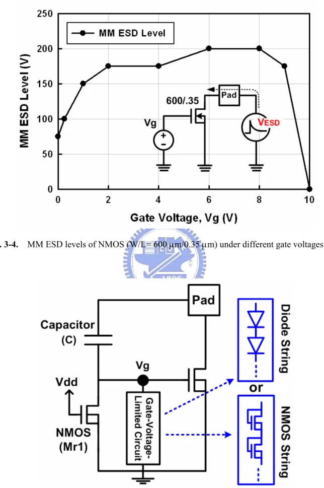
To practically investigate the over-gate-driven effect, the MM ESD levels of NMOS fabricated in a 0.35-μm CMOS process with gate-oxide thickness of ~75Å are tested under different gate voltages. The failure criteria of tested devices are judged by the leakage current over 1 μA under 3.3 V drain bias. The tested NMOS devices have device dimension of 600 μm/0.35 μm with each finger width of 30 μm. As shown in Fig. 3-4, when the gate voltage is 0 V (namely the GGNMOS), the non-uniform turn-on behavior causes a lower MM ESD level. With the increase of gate voltage up to 2 V, the non-uniform turn-on behavior can be diminished, and therefore the MM ESD level increases because more fingers of NMOS can be turned on to shunt ESD current. When the gate voltage is larger than 2 V, the trend of increase on MM ESD level is limited because all fingers have been fully triggered into snapback during ESD stress. When the gate bias voltage is over 8 V, the MM ESD level is dropped down dramatically due to the over-gate-driven effect in this 0.35-μm CMOS process.
3.3.
C
IRCUITS
OLUTION TOO
VERCOME THEO
VER-G
ATE-D
RIVENE
FFECT3.3.1 Design Concept
Since the over-gate-driven effect results from the over-coupled transient voltage at the gate of GCNMOS during ESD stress, this unwanted effect can be successfully overcome by a gate-voltage-limited circuit, which is added between the gate and the source of GCNMOS, to clamp the coupled gate voltage to a desired voltage level during ESD stress. In this work, the diodes or NMOS connected in series are used to realize the gate-voltage-limited circuit, as shown in Fig. 3-5. The coupled gate voltage on the GCNMOS during ESD stress can be controlled by varying the number and the device dimension of stacked diodes (or NMOS). Ideally, with the gate-voltage-limited diode (or NMOS) string, the coupled gate voltage (Vg) of GCNMOS during ESD stress can be clamped at Vt × n, where n and Vt are the number and the threshold voltage of the clamping device, respectively.
3.3.2 Gate Voltage Monitor Circuit
To verify the effectiveness of the proposed gate-voltage-limited circuit, a special on-chip gate voltage monitor circuit is added onto GCNMOS to monitor the coupled gate voltage (Vg) of GCNMOS during ESD stress. To monitor the gate voltage of GCNMOS under different transient voltages, the parasitic capacitance in the measurement setup should be minimized. The gate of GCNMOS cannot be directly connected to a bond pad or a voltage probe because the parasitic capacitance of the bond pad and the measurement instrument will affect the quantity of the coupled gate voltage on GCNMOS during ESD transition to cause the monitored gate voltage different from the practical cases. The special gate voltage monitor circuit is made up of an on-chip NMOS Mn2 and an external resistor Rext, as shown in Fig. 3-6. The device dimension
(W/L) of Mn2 is 10 μm/1 μm and the resistance of Rext is 1 kΩ. The gate of Mn2 and the gate of
using this gate voltage monitor circuit, the parasitic capacitance from Mn2 that affects the quantity of coupled gate voltage on GCNMOS is small enough to be negligible.
With the gate voltage monitor circuit, the coupled gate voltage of GCNMOS can be monitored through the drain voltage of Mn2 (indicated as Vdet in Fig. 3-6). When a voltage pulse is applied to
the pad, the gate voltage of GCNMOS is coupled high through the capacitor C. If the gate voltage of GCNMOS, which is the same potential of the gate voltage of Mn2, is not lifted greater than the threshold voltage of Mn2 (VtMn2), Mn2 is kept off and Vdet voltage is biased at 3 V through Rext.
When the gate voltage of GCNMOS is coupled higher than VtMn2, Mn2 is turned on to drop the
potential on Vdet from 3 V to (3 V – IMn2 × 1 kΩ), where IMn2 is the current flowing through Mn2.
Vg can be figured out with the help of HSPICE simulation because the gate voltage of an NMOS device is a function of its drain current. Therefore, the gate voltage of GCNMOS can be estimated from the Vdet voltage of the gate voltage monitor circuit and the HSPICE simulation.
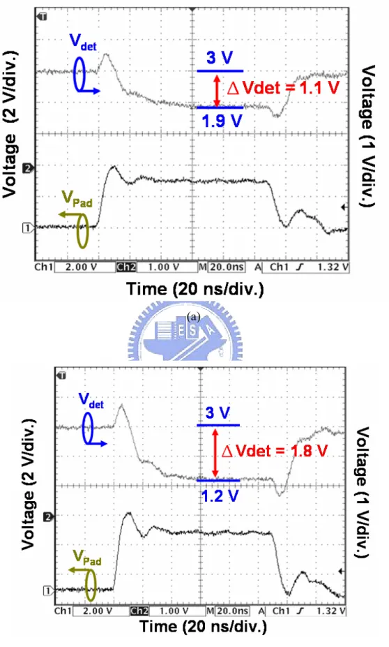
Figs. 3-7(a) and 3-7(b) show the measured results of the gate voltage monitor circuit on a GCNMOS without the gate-voltage-limited circuit. As shown in Fig. 3-7(a), when a 10-V voltage pulse was applied to the pad, the coupled Vg turned on Mn2 and the voltage on Vdet dropped from
3 V to 1.9 V. IMn2 can be calculated from (3 V-Vdet)/Rext as 1.1 mA. When a 15-V voltage pulse
was applied, because there was no gate-voltage-limited circuit added to the GCNMOS, the coupled gate voltage of GCNMOS was higher than that when a 10-V voltage pulse was applied. Therefore, Vdet voltage dropped from 3 V to a lower value, 1.2 V, as shown in Fig. 3-7(b), whereas the IMn2 is
calculated as 1.8 mA. From the HSPICE-simulated Id-Vg curve of the gate voltage monitor circuit, as shown in Fig. 8, GCNMOS without gate-voltage-limited circuit under 10-V and 15-V voltage pulses has the peak voltages of 1.85 V and 2.45 V, respectively. If no gate-voltage-limited circuit is added to GCNMOS, the larger ESD voltage pulse results in the higher coupled gate voltage on GCNMOS to suffer the over-gate-driven effect.
3.4. E
XPERIMENTALR
ESULTSIn this work, the gate-voltage-limited circuit is realized by the stacked diode string or the stacked NMOS string with different numbers or different dimensions. Every NMOS (diode) in the stacked NMOS (diode) string has the same device dimension. The GCNMOS is realized with a 3-pF coupling capacitor and an NMOS device (W/L) of 30 μm/1.5 μm, whose gate is connected to Vdd. The gate voltage monitor circuit is added to every GCNMOS for further exploring the effectiveness of the gate-voltage-limited circuit. ESD levels of GCNMOS were measured by ZapMaster and the tested devices were stressed by three continuous ESD zaps at every ESD test level under positive-to-VSS mode. The failure criteria of tested devices were judged by the leakage current over 1 μA under 3.3-V drain bias.
3.4.1. Clamping by NMOS String
To verify the effectiveness of the gate-voltage-limited circuit, voltage pulses with different pulse heights were applied to GCNMOS with the stacked NMOS string, which consists of two stacked 50 μm/0.35 μm NMOS. When a 10-V voltage pulse with a rise time of 10 ns was applied to GCNMOS, the Vdet voltage dropped from 3 V to 2.3 V with a ΔVdet of 0.7 V, as shown in Fig.
3-9(a). When the applied voltage pulse was increased to 20 V, the maximum ΔVdet was still 0.7 V,
as shown in Fig. 3-9(b). The applied voltage pulse with a larger pulse height results in a larger overshooting peak voltage coupled to the gate of GCNMOS. More charges are expected to be coupled to the gate of GCNMOS when a 20-V voltage pulse was applied on the GCNMOS. However, the measured ΔVdet between Figs. 3-9(a) and 3-9(b) do not increase when the applied
voltage pulse has the larger pulse height. Moreover, the ΔVdet of 0.7 V represents the IMn2 of 0.7
mA and the Vg voltage of 1.5 V, which is smaller than the Vg voltage of 2.45 V when a 15-V voltage pulse was applied on the GCNMOS without gate-voltage-limited circuit. Thus, the gate voltage of GCNMOS is successfully clamped by the gate-voltage-limited circuit.
For the GCNMOS with gate-voltage-limited circuit, the voltage coupled on its gate during ESD stress can be easily modulated by varying the number of stacked NMOS devices (or diodes). When the gate-voltage-limited circuits consist of more stacked NMOS devices, it is expected that a higher coupled voltage will stay on the gate of GCNMOS during ESD stress. Voltage pulses with 20-V pulse height and rise time of 10 ns were applied on GCNMOS with three or five stacked NMOS devices to measure the clamping voltage across the NMOS strings. When the GCNMOS has three (five) stacked NMOS devices in the gate-voltage-limited circuit, the measured ΔVdet is
1.4 V (2 V), as shown in Fig. 3-10(a) (Fig. 3-10(b)). From the voltage waveforms shown in Figs. 3-9(b), 3-10(a), and 3-10(b), the gate voltages of GCNMOS with two, three, and five stacked NMOS devices can be clamped to 1.5 V, 2.1 V, and 2.9 V, respectively, under the stress of a 20-V voltage pulse.
Since the gate voltage on GCNMOS can be modulated by varying the stacked NMOS devices (or diodes) in the gate-voltage-limited circuit, when a process has devices with thinner gate oxide, the number of stacked NMOS devices should be decreased to avoid the over-gate-driven effect. Therefore, the gate-voltage-limited circuit is portable between different CMOS technologies without modifying process steps or mask layers. Moreover, with a limited gate voltage on the GCNMOS during ESD stress, the optimization of gate-coupled design for GCNMOS becomes simpler.
Ideally, during ESD stress, the gate-voltage-limited circuit can clamp the gate voltage of GCNMOS at its total cut-in voltage, Vt × n, where n is the number and Vt is the threshold voltage of NMOS (diode). However, the equation of Vt × n should be modified to [(Vt × n) + (ION ×
RON)], where ION is the current flowing through the gate-voltage-limited circuit and RON is the
turn-on resistance of the NMOS string.
Voltage pulses with 20-V pulse height and rise time of 10 ns were applied on two GCNMOS with different sizes of stacked NMOS devices in the gate-voltage-limited circuits. Both of the GCNMOS have three stacked NMOS devices in their gate-voltage-limited circuit. However, one
of the gate-voltage-limited circuits consists of NMOS string where each NMOS device has device dimension of 50 μm/0.35 μm. The other consists of NMOS string where each NMOS device has device dimension of 20 μm/0.35 μm. When 20-V voltage pulses were applied to the two GCNMOS, the measured Vdet waveforms are shown in Fig. 3-11, where difference of 0.2 V is
found between the Vdet voltages. The gate-voltage-limited circuit which consists of NMOS devices
with smaller device dimension results in the lower Vdet voltage, and therefore has the larger IMn2
and the higher gate voltage of GCNMOS during ESD stress. This result is owing to the larger turn-on resistance of smaller NMOS device dimension in the gate-voltage-limited circuit. From the Id-Vg curve shown in Fig. 3-8, the 0.2 V voltage difference on Vdet represents a voltage difference
of 0.15 V on the gate voltage of GCNMOS. In nano-scale CMOS technologies, to limit the gate voltage of GCNMOS within the small design window, where the over-gate-driven effect is minimized or nullified during ESD stress, can be easily achieved by varying the device dimension and the device number of stacked NMOS (diode) devices in the gate-voltage-limited circuit.
Comparing the MM and HBM ESD stresses, the MM ESD stress with fast transition is more sensitive to suffer the over-gate-driven effect. The MM ESD levels per square micrometer of GCNMOS with different NMOS strings are shown in Fig. 3-12. For GCNMOS without the NMOS string, it has the lowest MM ESD level of 490 V. This lowest MM ESD level apparently does not result from the non-uniform turn-on behavior but the over-gate-driven effect, because the gate-coupled technique has been applied on the GCNMOS. With the NMOS string, a 30% increase on the MM ESD level of GCNMOS has been achieved. As shown in Fig. 3-12, the highest MM ESD level of GCNMOS is increased from 490 V to 645 V.
Comparing the MM ESD levels of GCNMOS with different numbers or different sizes of stacked NMOS devices, the trend of these curves is consistent with the characteristics of the gate-voltage-limited circuit. The more number of stacked NMOS devices in the gate-voltage-limited circuit results in the higher MM ESD level because the higher clamped gate voltage can further trigger on more fingers of GCNMOS during ESD stress. For the smaller
NMOS device dimension in the gate-voltage-limited circuit, it has larger turn-on resistance, resulting in the higher gate voltage to trigger on more fingers of GCNMOS during ESD stress. Therefore, under the same number of stacked NMOS devices, the NMOS devices with smaller device dimension in the gate-voltage-limited circuit result in the higher MM ESD level.
When the gate-voltage-limited circuit is composed of five stacked NMOS devices, the clamped gate voltage of GCNMOS during ESD stress is too high to overcome the over-gate-driven effect. Therefore, the MM ESD levels degrade again, except for the gate-voltage-limited circuit with the largest NMOS device dimension of 70 μm/0.35 μm. The gate-voltage-limited circuit with five stacked NMOS devices of 70 μm/0.35 μm can still protect GCNMOS from the over-gate-driven effect due to its lowest turn-on resistance to limit the over-coupled gate voltage on GCNMOS during ESD stress. For GCNMOS under HBM ESD stress which has slow ESD transition due to the 1.5-kΩ resistor in its discharging path, every GCNMOS (both with and without the gate-voltage-limited circuit) can pass 8-kV HBM ESD stress because the multiple fingers of GCNMOS with a large device dimension of 600 μm/0.35 μm can be uniformly triggered on by the gate-coupled design.
To further support the effectiveness of the gate-voltage-limited circuit on MM ESD levels shown in Fig. 3-12, failure analyses on these failed GCNMOS were carried out through the scanning electron microscope (SEM) images. Fig. 3-13 shows the ESD failure location of GCNMOS with gate-voltage-limited circuit, which consists of two stacked NMOS devices with each device dimension of 70 μm/0.35 μm. Because the over-gate-driven effect is overcome by the gate-voltage-limited circuit, the drain-substrate junction of the GCNMOS was damaged by MM ESD stress but its gate oxide is still intact.
When GCNMOS has five stacked NMOS devices with each device dimension of 20 μm/0.35 μm, its MM ESD level is degraded, as shown in Fig. 3-12. The SEM image shown in Fig. 3-14(a) indicates that the gate of this GCNMOS was damaged by the ESD current, supporting the interpretation that the over-gate-driven effect causes such ESD failure on this GCNMOS. The
image of its ESD failure location on the gate is enlarged in Fig. 3-14(b).
For GCNMOS with five stacked NMOS devices with each device dimension of 70 μm/0.35 μm, its MM ESD level is still increased, as shown in Fig. 3-12. The ESD failure on this GCNMOS has been found at the drain-substrate junction instead of its gate oxide, indicating that the over-gate-driven effect can still be overcome due to the lowest turn-on resistance of the NMOS string with larger device size. Fig. 3-15(b) shows the enlarged image of its ESD failure location on the drain contacts. From these visual evidences, the effectiveness of the gate-voltage-limited circuit has been strongly confirmed.
3.4.2 Clamping by Diode String
The other implementation of the gate-voltage-limited circuit in this work is with the diode string, composed of stacked diodes with different numbers and different device dimensions. The diode string has similar characteristics to that of the clamping NMOS string. The larger number of stacked diodes in the gate-voltage-limited circuit will cause the higher clamped gate voltage on GCNMOS during ESD stress. Turn-on resistance of the stacked diodes should be also finely tuned to control the gate voltage of GCNMOS during ESD stress.
The MM ESD levels of GCNMOS with different numbers or different device dimensions of stacked diodes are shown in Fig. 3-16. The larger number and the smaller device dimension of the stacked diodes in the diode string result in the higher MM ESD level, which has a higher coupled gate voltage to help the turn-on uniformity of GCNMOS. With the diode string, the highest MM ESD level of GCNMOS is 645 V, which is a 30% increase compared with that of GCNMOS without the gate-voltage-limited circuit. When the number of stacked diodes with device dimension of 25×25 μm2 in the gate-voltage-limited circuit is increased up to 3, the MM ESD
level becomes saturated, as shown in Fig. 3-16. This implies that somewhat over-gate-driven effect was initiated in the GCNMOS. If the diode device dimension is enlarged, the MM ESD level becomes increased again. So, the over-gate-driven effect can be successfully overcome by circuit
design technique without involving the process modification. The ESD robustness of GCNMOS can be optimized in different CMOS processes by the proposed circuit design technique.
3.5 C
ONCLUSIONThe effectiveness and the characteristics of the proposed gate-voltage-limited circuit have been successfully verified. The new proposed ESD design method with the gate-voltage-limited circuit can successfully prevent the over-gate-driven effect and continually improve the ESD level of ESD protection circuits with the gate-coupled or gate-driven technique in the sub-quarter-micron CMOS processes. From the experimental results in a 0.35-μm CMOS process, a 30% increase of MM ESD robustness of GCNMOS has been achieved by adding the gate-voltage-limited circuit to the GCNMOS. The new proposed portable design method provides a high flexibility to realize the gate-voltage-limited circuit in different CMOS processes without process modification to save the fabrication cost of IC products.
Fig. 3-1. The TLP-measured I-V characteristic of GGNMOS fabricated in a 0.35-µm CMOS
technology.
(a) (b)
Fig. 3-2. Two traditional circuit design methods to carry out the gate-coupled technique and to
(a)
(b)
Fig. 3-3. The simulated current flow lines of NMOS with a bipolar trigger voltage of 5.7 V.
Voltages applied to drain and gate electrodes are respectively ramped to 6.5 V and 2 V with simultaneous rise time of (a) 10 ns, and (b) 5 ns.
Fig. 3-4. MM ESD levels of NMOS (W/L= 600 μm/0.35 μm) under different gate voltages.
Fig. 3-6. The gate voltage monitor circuit added on-chip can monitor Vg of GCNMOS during
(a)
(b)
(a)
(b)
Fig. 3-9. The measured Vdet voltages when (a) 10-V, and (b) 20-V, voltage pulse with a rise time
(a)
(b)
Fig. 3-10. The measured Vdet voltages when the 20-V voltage pulse with a rise time of 10 ns is
applied to GCNMOS with (a) three, and (b) five, stacked NMOS devices in the gate-voltage-limited circuit. Each stacked NMOS has a device dimension (W/L) of 50 μm/0.35 μm.
Fig. 3-11. The measured Vdet voltages when 20-V voltage pulses with rise time of 10 ns are
applied to GCNMOS with two different gate-voltage-limited circuits. One consists of three stacked NMOS devices with each device dimension (W/L) of 20 μm/0.35 μm, the other consists of three stacked NMOS devices with each device dimension of 50 μm/0.35 μm.
Fig. 3-12. MM ESD levels of the GCNMOS with different numbers or different device
Fig. 3-13. SEM image of the GCNMOS with two stacked NMOS devices in the
gate-voltage-limited circuit after 550-V MM ESD stress. Each stacked NMOS has device dimension (W/L) of 70 μm/0.35 μm.
(a)
(b)
Fig. 3-14. SEM image of (a) the GCNMOS with five stacked NMOS devices in the
gate-voltage-limited circuit after 600-V MM ESD stress. Each stacked NMOS has device dimension (W/L) of 20 μm/0.35 μm. (b) The enlarged image of its ESD failure location.