國 立 交 通 大 學
電子工程學系 電子研究所碩士班
碩 士 論 文
臨場共製之 REFET 與 ISFET 對於感測氧化層厚度調變的
飄移特性之研究
The Study of Drift Characteristics
with Sense Oxide Thickness Modulation
by Co-Fabricating REFET and ISFET
學生: 徐信佑
Student: Hsin-Yu Hsu
指導教授: 張國明 博士
Advisor: Dr. Kow-Ming Chang
臨場共製之 REFET 與 ISFET 對於感測氧化層厚度調變的
飄移特性之研究
The Study of Drift Characteristics
with Sense Oxide Thickness Modulation
by Co-Fabricating REFET and ISFET
研 究 生:徐信佑 Student:Hsin-Yu Hsu
指導教授:張國明 博士 Advisor:Kow-Ming Chang
國 立 交 通 大 學
電 子 工 程 學 系
碩 士 論 文
A ThesisSubmitted to Department of Electronics Engineering & Institute of Electronics College of Electrical Engineering and Computer Science
National Chiao Tung University in Partial Fulfillment of the Requirements
for the Degree of Master of Science
in
Electronics Engineering June 2006
Hsinchu, Taiwan, Republic of China
臨場共製之 REFET 與 ISFET 對於感測氧化層厚度調變的
飄移特性之研究
學生:徐信佑 指導教授:張國明 博士
國立交通大學
電子工程學系 電子研究所碩士班
摘 要
本論文係利用電漿輔助化學氣象沈積的二氧化矽當作離子感測電晶體的 感測材料,以及利用濺鍍的五氧化二鉭當作參照電晶體的感測材料,來研究其 感測度及飄移特性。由此兩種材料製成的感測電晶體的感測度顯示,其感測特 性主要是由材料的表面特性所影響。但是其飄移特性則是由材料的塊材特性所 決定。飄移現象的產生是因為感測層材料表面的水合作用,以及氫離子在水合 層中的殘留所造成。電漿輔助化學氣象沈積的二氧化矽材料會導致嚴重的水合 作用,因此以此材料當作感測層的離子感測電晶體相對於其他材料的離子感測 電晶體而言,會產生明顯的閘極電壓飄移現象。六小時的量測結果顯示,電漿 輔助化學氣象沈積的二氧化矽材料層的水合深度大約是 500 埃,並且最大的閘 極電壓飄移是 81 毫伏。The Study of Drift Characteristics with Sense Oxide
Thickness Modulation by Co-Fabricating REFET and
ISFET
Student: Hsin-Yu Hsu Advisor: Dr. Kow-Ming Chang
Department of Electronics Engineering & Institute of Electronics
National Chiao Tung University
ABSTRACT
The ISFETs of PECVD SiO2 as the sensing membrane and the REFETs with a
sensing layer of sputtered Ta2O5 were fabricated to study the sensitivity and the drift
characteristics. The sensitivity characteristics of SiO2-gate ISFETs and Ta2O5-gate
REFETs showed that the pH responses were dependent on the surface characteristics of materials. But the drift characteristics were dependent on the characteristics of the material bulks. The drift phenomenon was due to the hydration effect of the sensing layer surface and the contamination of hydrogen ions in the hydrated layer. PECVD deposited SiO2 can lead to a critical hydration effect such
that the gate voltage drift of a PECVD SiO2-gate ISFET is obvious relative to other
ISFETs with sensing layers of different materials. In the measurement with duration of 6 hours, the hydration depth of a PECVD SiO2 layer was about 500Å and the
誌 謝
能完成此一論文,首先要感謝的是張國明老師能讓我有機會參與 ISFET 的 研究,並且提供一個資源豐富的研究環境讓我得以在短時間內完成論文。老師 對學生的關心與照顧,是讓我得以在挫敗中重新站起來的最大助力,張老師也 是我今生永遠不會忘記的恩師。 其次要感謝的是趙高毅學長對此論文實驗部分的完善規劃,以及對此研究 過程中對於遇到的問題提供非常有幫助的建議與討論,使得研究能夠順利進行 並且達到預期的實驗成果。 另外我還要感謝庭暐在實驗製程上的幫助以及經驗上的分享,讓我得以順 利的完成實驗;還有感謝知天學長在歷次的討論當中所提出來很有幫助性的討 論內容,讓我得以在短時間內能夠快速瞭解 ISFET 的內涵。 最後還要感謝閔媛以及在我最低潮的時候給我鼓勵與支持的所有學長與 同學,讓我能有勇氣能繼續完成此論文。衷心的感謝與祝福所有陪伴我一起走 過碩士班生涯的每個人,有你們的幫助才是我完成碩士論文的最大動力來源!Contents
Abstract
(in Chinese)
……….. iAbstract
(in English)
……….. iiAcknowledgement
……….. iiiContents
……….. ivTable Captions
……….. vFigure Captions
……….. viChapter 1
Introduction
……… 11.1 The Importance of pH Detection………. 1
1.2 Techniques for pH Detection……….. 1
1.3 The Problem of pH ISFET and the Investigation of this Problem……… 2
Chapter 2
Theories for the Investigation of Drift
Characteristics
………... 42.0 Introduction………. 4
2.1 Fundamental Principles of ISFET……… 4
2.1.1 From MOSFET to ISFET……… 4
2.1.2 The pH Response at Oxide-Electrolyte Interface……… 6
2.2 Drift Phenomenon……… 7
2.3 Physical Model for Drift……….. 8
2.3.1 Dispersive Transport……… 8
2.3.2 Expression for Drift………. 9
Chapter 3
Experiment and Measurement
………. 123.0 Introduction……….. 12 3.1 Differential Sensing………. 12 3.1.1 Reference Electrode………. 12 3.1.2 Reference FET………. 13 3.2 Fabrication Process……….. 13 3.3 Measurement Principle……… 15
Chapter 4
Results and Discussions
……….. 164.1 Sensitivities of PECVD SiO2 and Sputtered Ta2O5…………. 16
4.2 Drift Characteristics………. 17
4.3 Conclusions……….. 18
Chapter 5
Future Work
………... 205.1 Electric Field Enhanced Migration of Hydrogen Ions………. 20
References
……….. 21Table Captions
Table 4-1 SiO2 and Ta2O5 responses to pH electrolyte………... 39
Figure Captions
Figure 2-1 Schematic representation of (a) MOSFET, (b) ISFET………... 23
Figure 2-2 Series combination of the (a) initial (b) hydrated insulator capacitance……….. 23
Figure 3-1 Fabrication process flow………. 25
Figure 3-2 Measurement setup………. 25
Figure 3-3 Detection principle of pH……… 26
Figure 3-4 Detection principle of drift……….. 26
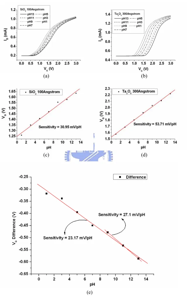
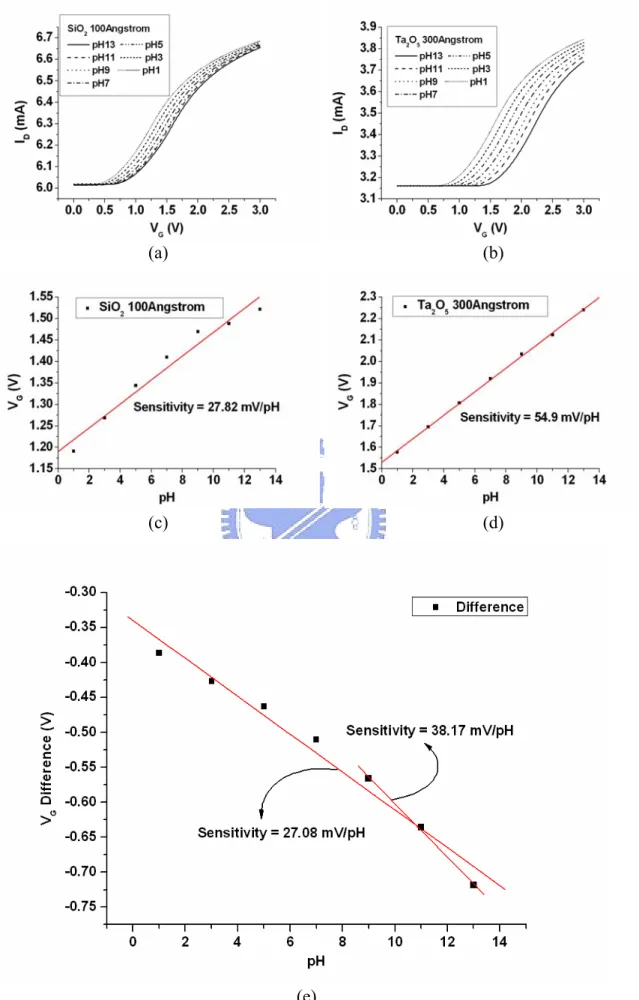
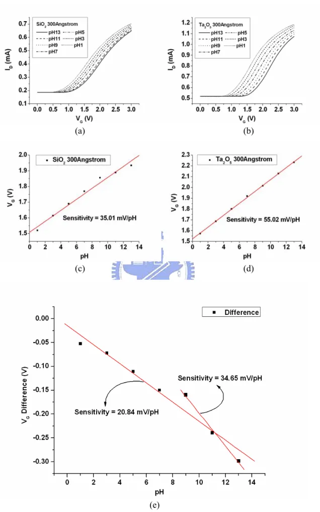
Figure 4-1 Sensitivities of ISFET and REFET with xU=100Å, W/L=400μm/20μm……….. 27
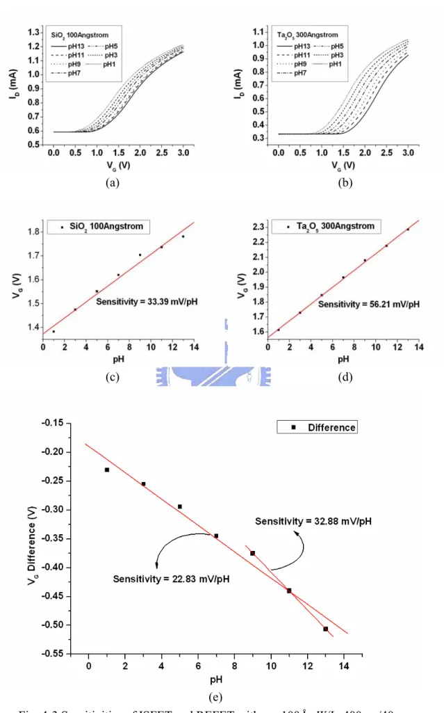
Figure 4-2 Sensitivities of ISFET and REFET with xU=100Å, W/L=400μm/30μm……….. 28
Figure 4-3 Sensitivities of ISFET and REFET with xU=100Å, W/L=400μm/40μm……….. 29
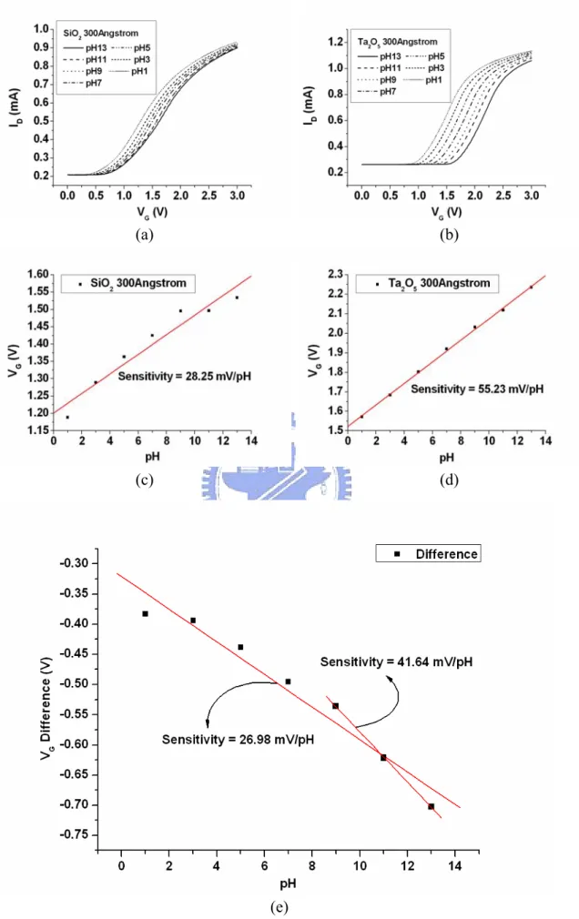
Figure 4-4 Sensitivities of ISFET and REFET with xU=300Å, W/L=400μm/20μm……….. 30
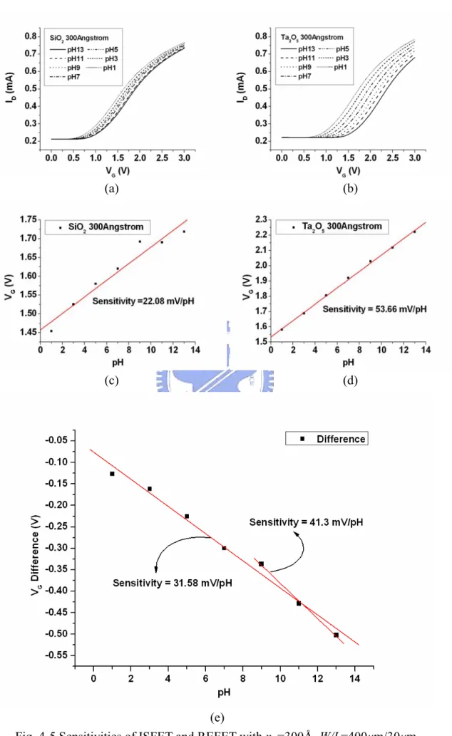
Figure 4-5 Sensitivities of ISFET and REFET with xU=300Å, W/L=400μm/30μm……….. 31
Figure 4-6 Sensitivities of ISFET and REFET with xU=300Å, W/L=400μm/40μm……….. 32
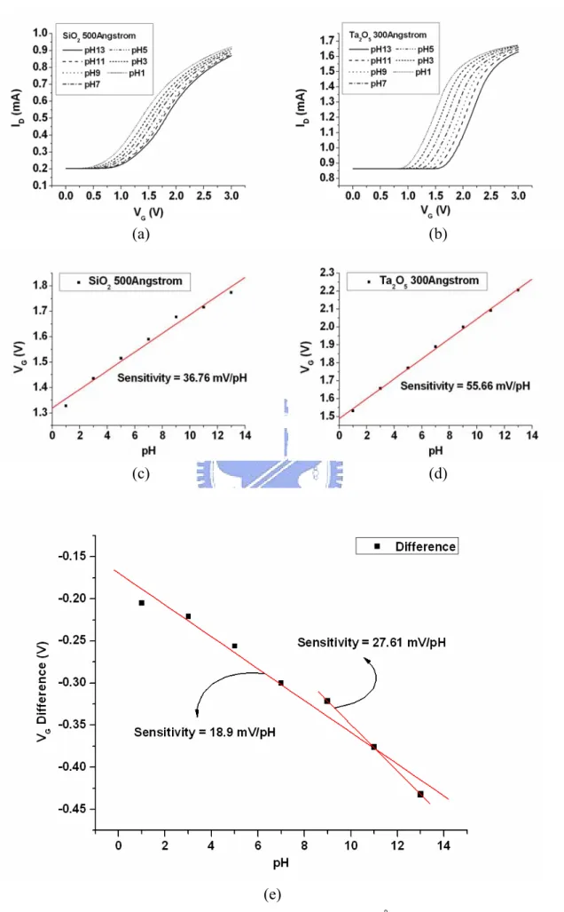
Figure 4-7 Sensitivities of ISFET and REFET with xU=500Å, W/L=400μm/20μm……….. 33
Figure 4-8 Sensitivities of ISFET and REFET with xU=500Å, W/L=400μm/30μm……….. 34
Figure 4-9 Sensitivities of ISFET and REFET with xU=500Å, W/L=400μm/40μm……….. 35
Figure 4-10 Sensitivities of ISFET and REFET with xU=1000Å, W/L=400μm/20μm……….. 36
Figure 4-11 Sensitivities of ISFET and REFET with xU=1000Å, W/L=400μm/30μm……….. 37
Figure 4-12 Sensitivities of ISFET and REFET with xU=1000Å, W/L=400μm/40μm……….. 38
Figure 4-13 Drift characteristics of the 100Å PECVD SiO2-gate ISFET………….. 40
Figure 4-14 Drift characteristics of the 300Å PECVD SiO2-gate ISFET………….. 40
Figure 4-15 Drift characteristics of the 500Å PECVD SiO2-gate ISFET………….. 41
Figure 4-16 Drift characteristics of the 1000Å PECVD SiO2-gate ISFET………… 41
Figure 4-17 Average drift of the PECVD SiO2-gate ISFET during the last 5 hour………. 42
Figure 4-18 Drift characteristics of the 300Å Ta2O5-gate ISFET……….. 42
Figure 4-19 ID-VD curve of the 100Å SiO2-gate ISFET………. 44
Figure 4-20 ID-VD curve of the 300Å SiO2-gate ISFET………. 44
Figure 4-21 ID-VD curve of the 500Å SiO2-gate ISFET………. 45
Figure 4-22 ID-VD curve of the 1000Å SiO2-gate ISFET………... 45
Chapter 1
Introduction
1.1 The Importance of pH Detection
pH is one of the most common laboratory measurements because so many chemical and biomedical process are dependent on pH [1].
(1) Both the solubility of many chemicals or biomolecules in solution and the speed or rate of (bio-)chemical reactions are dependent on pH.
(2) The body fluid of living organisms usually has specific pH range that can reflect the health situation of the body. The pH values of lakes, rivers, oceans and soil differ and depend on the kinds of animals and plants living there. The wastewater from factories and households may cause the pH changes of water and cause the destruction of the environment.
(3) All the industries that deal with water: from the drinking water, the food and the drugs to the paper, plastics, semiconductors, cements, glass or textiles.
1.2 Techniques for pH Detection
Traditionally, the methods for the measurement of pH values include indicator reagents, pH test strips, metal electrode and glass electrode. Because of some limitations in practical applications of the first three methods, the glass electrode becomes the most widely used method for the pH measurement, and it is considered to be the standard measuring method.
Nernstian response independent of redox interferences, short balancing time of electrical potential, high reproducibility and long lifetime. However, glass electrode has several drawbacks for many industrial applications. Firstly, they are unstable in alkaline or HF solutions or at temperatures higher than 100°C. Also, they exhibit a sluggish response and are difficult to miniaturize. Moreover, they cannot be used in food or in in vivo applications due to their brittle nature [1]. There is an increasing need for alternative pH electrodes.
New trends of pH measurements include optical-fiber-based pH sensor, mass-sensitive pH sensor, metal oxide sensor, conducting polymer pH sensor, nano-constructed cantilever-based pH sensor, ISFET-based pH sensor and pH-imaging sensor.
In this study, the problems in practical applications of ISFETs are continuing to be investigated.
1.3 The Problem of pH ISFET and the Investigation of this Problem
As mentioned in the first section, the environment of pH detection is always in a wet condition. That is, the devices used for the pH measurement must be immersed in the water solution, and then the sensing materials react with the solution and exhibit the pH responses. For ISFETs, the sensing materials used for pH detections are the gate oxides, such as SiO2, Si3N4, Ta2O5, Al2O3, etc., however, these materials are not
completely waterproof in nature. Some solution will permeate into the oxide surfaces and that may lead to the hydration effect. The hydration effect is a reaction correlated with time. The period of the hydration effect for Si3N4 to reach a steady state was
about 50-60 hours in pH 7 solution [2], and for Al2O3 was about 7 hours [2].
the commercialization speed and lowers the reliability of ISFET. Hydration can lead to a drift phenomenon of the gate voltage during the measurement, especially in the first two to three hours. When measuring the pH responses, the stability and accuracy are seriously influenced by the drift voltage.
In order to have a further understanding of the drift phenomenon, SiO2 grown by
plasma-enhanced chemical vapour deposition (PECVD) was used for the sensing layer of ISFET. PECVD SiO2 is relatively poor in structural integrity and is expected
to have an obvious hydration effect which can help us to observe the drift phenomenon more clearly. Detailed experiment steps will be presented in chapter 3, and the results will be discussed in chapter 4.
Chapter 2
Theories for the Investigation of Drift Characteristics
2.0 Introduction
In this chapter, the theories of metal oxide semiconductor field effect transistor (MOSFET) which are relevant to ISFET will firstly be presented. The fundamental principles of ISFET will be developed from these MOSFET theories. The pH response at the oxide-electrolyte interface will also be characterized in the first section. Subsequently, the drift phenomenon which is caused by the hydration effect and the ions transport in the insulator will be discussed. In the final section, a physical model for drift developed by Jamasb [12] will be presented. This model can help us to have a further understanding of the mechanism responsible for the instability of ISFET under long-term operating.
2.1 Fundamental Principles of ISFET
Since the first report of the ISFET by Bergveld, research on new material and fabrication process to improve the sensitivity and stability has been continuously proposed [3-5]. At the same time, the mechanism of the pH response of pH ISFET has also been studied extensively [4-10]. The followings are the theoretical foundations which are mostly adopted to characterize the ISFET.
Seen by the history of the development of ISFET, it is not difficult to find out the similarities between ISFET and MOSFET. The most obvious characteristic is the similarity between their structures. Therefore, the best way to comprehend the ISFET is to understand the operating principle of a MOSFET first. When MOSFET is operated in the so-called ohmic or non-saturated region, the drain current ID is given
by:
(
GS T)
DS DS OX D V V V V L W C I ⎭ ⎬ ⎫ ⎩ ⎨ ⎧ − − = 2 1 μ (2-1) where COX is the gate insulator capacitance per unit area, μ the electron mobility in the channel and W/L the width-to-length ratio of the channel.The threshold voltage VT of Eq. (2-1) is described by the following expression:
F OX B FB T C Q V V = − +2φ (2-2)
where VFB is the flat-band voltage, QB the depletion charge in the substrate, and B ψF
the potential difference between the Fermi levels of doped and intrinsic silicon. For a MOSFET with charge present in the oxide and at the oxide-semiconductor interface, the flat-band voltage can be given by:
OX SS OX Si M FB C Q Q q V = Φ −Φ − + (2-3)
where ΦM is the workfunction of the gate metal, ΦSi the workfunction of silicon, QOX the charge in the oxide and QSS the surface state density at the oxide-silicon interface. Substitution of Eq. (2-3) in Eq. (2-2), the general form of the threshold voltage of a MOSFET becomes: F OX B SS OX Si M T φ C Q Q Q q V =Φ −Φ − + + +2 (2-4)
This equation holds true for the metal gate MOSFET. But in case of the ISFET, the metal gate is no longer present, so that the term ΦM/q must be revised. Figure 2-1 illustrates the similarities and differences between these two devices. It can be seen
that the reference electrode, the aqueous solution and the phenomena occurring at the oxide-solution interface must be accounted for instead of ΦM/q. Hence the threshold voltage of the ISFET becomes:
F OX B SS OX Si sol ref T φ C Q Q Q q Ψ χ E V = + − 0 −Φ − + + +2 (2-5)
where Eref represents the constant potential of the reference electrode, χsol is the surface dipole potential of the solution which also has a constant value. The term Ψ0 representing the surface potential at the oxide-electrolyte interface is the key element that makes ISFET pH-sensitive.
2.1.2 The pH Response at Oxide-Electrolyte Interface
The surface of any metal oxide always contains hydroxyl groups, in the case of silicon dioxide SiOH groups. These groups can be protonated and deprotonated, and thus, when the gate oxide contacts an aqueous solution, a change of pH will change the SiO2 surface potential. These reactions can be expressed by
+ ++ ←⎯→ 2 1 SiOH SiOH H K S (2-6) + + ⎯→ ←K SiO- HS SiOH 2 (2-7)
where HS+ represents the protons at the surface of the oxide.
The pH response, which is generally called the sensitivity, is defined as the surface potential change over a pH unit change. This response is given by
α q kT . δpH δΨ B 3 2 0 =− (2-8) with 1 3 2 1 int 2 + = β q kTC . α dif (2-9)
where pHB is the pH value in the solution bulk, k is the Boltzmann constant, T is the absolute temperature, C
B
dif is the differential capacitance, and βint is the intrinsic buffer capacity. α is a dimensionless sensitivity parameter. The value of α varies between 0 and 1 depending on the intrinsic buffer capacity and the differential capacitance. If α equals 1, the theoretical maximum sensitivity of -59.2mV/pH at room temperature can be obtained.
The potential between electrolyte solution and insulator surface causes a proton concentration difference between bulk and surface that is according to Boltzmann:
kT qΨ a a B S H H 0 exp− = + + (2-10)
where + and are the activity of H S
H
a +
B
H
a + at the oxide surface and in the solution
bulk, respectively. According to the definition of pH, Eq. (2-10) can be expressed by
kT qΨ pH pHS B 3 . 2 0 + = (2-11)
(2-11) correlates the pHS in (2-6) and (2-7) with the pHB in (2-8).
2.2 Drift Phenomenon
Drift phenomenon can be considered by two aspects of view, the hydration of the insulator surface after immersing it in pH buffer solution, and the trap of hydrogen-bearing species by the binding sites when they transport through the insulator. The former’s influence on drift is generally smaller than the latter. This result can be found in the previous work [2, 11-13] and also in the measurement data of this research. The following models, which are classified according to the location where the mechanism of pH-sensitivity is presumed to occur, will help us to have a further understanding of the transport of mobile ions [14]:
the insulator react with ions in the solution and build up a surface potential. This will lead to the formation of the electrical double layer in the electrolyte at the interface with the insulator. This model is generally regarded as the site-binding model.
(2) Models based on the presence of mobile ions in the insulating layer. This implies the existence of a transport mechanism to establish the required thermodynamic equilibrium, and leads directly to a Nernst equation. This model is generally regarded as the gel model.
(3) Models based on the modification of the Si/SiO2 interface through a
pH-controlled change in the surface state density via transport of a hydrogen-bearing species.
The above discussions are only the characteristics of ions transport in the insulator, while the physical model for the gate voltage drift is going to be presented in the next section.
2.3 Physical Model for Drift
The physical model for drift was firstly proposed by Jamasb in 1997 [11]. The key point of this model was that employing the dispersive transport theory to express the gate voltage drift which is caused by the hydration effect at the insulator-electrolyte interface.
2.3.1 Dispersive Transport
Dispersive transport was brief reviewed in [12] and it could be characterized by a power-law time decay of the mobility or diffusivity of the form tβ-1, 0<β<1. This time dependence is based on a model that interprets transport in terms of a “random walk”.
The origin of random walk is either a) hopping motion through localized states giving rise to hopping transport, or b) multiple trapping from a band of extended states or localized states leading to multiple-trap transport. The multiple-trap transport is generally associated with the motion of electrons or holes in disordered materials. Regardless of the specific dispersive mechanism involved, dispersive transport leads to a characteristic power-law time decay of diffusivity which can be described by 1 0 00( ) ) (t =D ω t β− D (2-12) where D00 is a temperature-dependent diffusion coefficient which obeys an Arrhenius
relationship, ω0 is the hopping attempt frequency, and β is the dispersion parameter
satisfying 0<β<1. Dispersive transport leads to a decay in the density of sites/traps occupied by the species undergoing transport. This decay is described by the stretched-exponential time dependence given by
] ) / exp[( ) 0 ( ) ( / / t N t τ β NS T =Δ S T − Δ (2-13)
where ΔNS/T(t) is the area density (units of cm-2) of sites/traps occupied, τ is the time constant associated with structural relaxation, and β is the dispersion parameter.
2.3.2 Expression for Drift
Since hydration leads to a change of the chemical composition of the sensing oxide surface, it is reasonable to assume that the dielectric constant of the hydrated surface layer differs from that of the sensing oxide bulk. The overall insulator capacitance, which is determined by the series combination of the surface hydration layer and the underlying oxide, will exhibit a slow, temporal change. When drift phenomenon occurs at the surface of an actively-biased ISFET, the gate voltage will
simultaneously exhibit a change to keep a constant drain current. The change of the gate voltage can be written as
) 0 ( ) ( ) ( G G G t V t V V = − Δ (2-14) Since the voltage drop inside of the semiconductor is kept constant, ΔVG(t) becomes
)] 0 ( ) ( [ )] 0 ( ) ( [ ) ( FB FB ins ins G t V t V V t V V = − + − Δ (2-15) where VFB is the flatband voltage and Vins is the voltage drop across the insulator. VFB and Vins are given by
OX SS OX Si sol ref FB C Q Q q Ψ E V = +χ − 0 −Φ − + (2-16) OX inv B ins C Q Q V = −( + ) (2-17)
where Qinv is the inversion charge. If the temperature, pH, and the ionic strength of the solution are held constant, Eref, χsol, Ψ0, and ΦSi can be neglected, so the drift can be
rewritten as ⎥ ⎦ ⎤ ⎢ ⎣ ⎡ − + + + − = Δ ) 0 ( 1 ) ( 1 ) ( ) ( I i inv B SS OX G C t C Q Q Q Q t V (2-18)
In this study, the gate oxide of the fabricated ISFET was composed of two layers, a lower layer of thermally-grown SiO2 of thickness, xL, and an upper layer of PECVD SiO2 of thickness, xU.. CI(0) is the effective insulator capacitance given by the series combination of the thermally-grown SiO2 capacitance, εL/xL, and the PECVD SiO2
capacitance, εU/xU. Ci(t) is analogous to CI(0), but an additional hydrated layer of capacitance, εHL/xHL, at the oxide-electrolyte interface must be took into consideration, and the PECVD SiO2 capacitance is now given by εU/[xU-xHL]. The series combinations of the capacitances are illustrated in Figure 2-2. Therefore, the drift is given by ) ( ) ( ) (t Q Q Q Q x t V HL HL U HL U inv B SS OX G ⎟⎟ ⎠ ⎞ ⎜⎜ ⎝ ⎛ − + + + − = Δ ε ε ε ε (2-19)
From this equation, we observed that drift is directly proportional to the thickness of the hydrated layer. By applying dispersive transport theory, an expression for xHL(t) is given by [12]
[
]
{
1 exp ( /τ)β}
) ( ) (t x t xHL = HL ∞ − − (2-20) with hydr D T S HL N A N D x β ωβ (0) ) ( / 1 0 00 Δ = ∞ − (2-21)where AD represents the cross-sectional area, and Nhydr is the average density of the hydrating species per unit volume of hydration layer. Thus, the overall expression for the gate voltage drift is
[
{
τ β ε ε ε ε ) / ( exp 1 ) ( ) ( ) (t Q Q Q Q x t V HL HL U HL U inv B SS OX G ⎟⎟ ∞ − − ⎠ ⎞ ⎜⎜ ⎝ ⎛ − + + + − = Δ]
}
(2-22)From this equation, we can expect that if the time of gate oxide immersing in the test-solution is long enough (determined by the constant τ ), the gate voltage drift will approach a constant value which is greatly dependent on the hydration depth,
Chapter 3
Experiment and Measurement
3.0 Introduction
In this chapter, the advantage of making differential measurements between an ISFET and a reference FET (REFET) will be interpreted in the first section. The importance of a stable reference electrode (RE) in the miniaturized device will also be discussed. The second section is the fabrication process flow of the ISFET and REFET devices which are used for investigating the drift characteristics. Finally, the measurement setup, and the detection principles of pH and drift will be presented.
3.1 Differential Sensing
How to detect a correct and consistent pH value is always the direction of research. Besides adopting materials that have good linearity, sensitivity, and stability, there are two important subjects in measurement that provide alternative ways to obtain a reliable pH value. One is the design of a stable reference electrode, the other is the introduction of a REFET.
3.1.1 Reference Electrode
An ideal reference electrode for use as the ISFET gate terminal should provide [15]
b) an electrode/solution potential difference (Eref) that does not vary with solution composition.
The conventional silver chloride or calomel electrode provides both of these functions by maintaining an electrochemical equilibrium with the solution. Novel techniques are to fabricate the reference electrodes in miniaturized dimensions [16,17]. The on-chip fabrication of a reference electrode with IC-compatible techniques would make ISFETs suitable for biomedical sensing because of the low cost, small size and rigidity.
3.1.2 Reference FET
An alternative technique to achieve consistent pH detections is through the co-fabricating of an ISFET and a REFET. An ideal REFET is a FET that insensitive to ions in pH measurement [18], but identical to the ISFET in terms of transconductance, thermal response, etc. The differential measurement between an ISFET and a REFET thus eliminates the variations of the environment, such as temperature, light, instable reference electrode/solution contact potential, etc.
In this study, an alternative approach to the implementation of a REFET is introduced. Ta2O5 is a material that exhibits good linearity, sensitivity, and stability in
the pH measurement, so we are trying to take this material as the sensing layer material instead of an ion-insensitive one.
3.2 Fabrication Process
As mentioned in the previous section, Ta2O5 was taken as the sensing layer
deposited by sputtering, and SiO2 was deposited using plasma-enhanced chemical
vapour deposition (PECVD). Because of the relatively low deposition temperature, PECVD SiO2 is poor in structural integrity in comparison with other preparation
methods, such as LPCVD and thermally grown silica [19]. The poor integrity of the gate oxide structure is expected to have an obvious hydration effect which can help us to observe the drift phenomenon more clearly during the pH measurement. The following is the procedure for fabricating the ISFET and REFET devices, and the process is illustrated in Figure 3-1:
a) RCA clean
Wet-oxidation, 6000Å, 1050°C b) Defining of S/D (mask 1) BOE wet-etching of SiO2
c) Dry-oxidation, 300Å, 1050°C S/D ion implantation
S/D annealing, 950°C, 60min d) PECVD SiO2 for passivation, 1μm
e) Defining of contact hole and gate region (mask 2) BOE wet-etching of SiO2
f) Dry growth of gate oxide, 100Å, 850°C
g) PECVD SiO2 as sensing layer, 4 conditions are prepared, 100Å, 300Å, 500Å,
1000Å
Defining of sensing region (mask 3) HF wet-etching of SiO2
h) Sputtering Ta2O5 as sensing layer, 300Å (mask 4)
Ta2O5 sintering, 600°C, 30min
Al sintering, 400°C, 30min
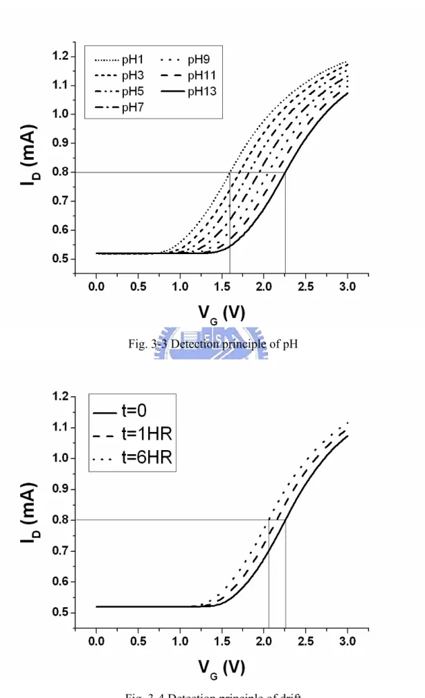
3.3 Measurement Principle
The setup of the measurement system is illustrated in Figure 3-2. ISFET and REFET were designed to share the same source terminal, and the drain-to-source voltage were biased at the same condition (VDS1=VDS2). The drain currents of ISFET
and REFET were set at a constant magnitude, therefore, if the pH of the solution varies, the gate voltage must adjust its magnitude to maintain the constant current. Consequently, the variation of the gate voltage exhibits the pH sensitivity of the sensing oxide. Figure 3-3 illustrates the detection principle of pH. For the drift measurement, the detection principle is in a similar manner to that of the pH measurement and is shown in Figure 3-4.
Chapter 4
Results and Discussions
4.1 Sensitivities of PECVD SiO
2and Sputtered Ta
2O
5Figure 4-1~4-12 are the measured sensitivities of PECVD SiO2 and sputtered
Ta2O5, and the data are sorted in Table 4-1. The samples of SiO2 were prepared in
dimensions of W/L=400μm/20μm, 400μm/30μm and 400μm/40μm as well as in thickness of 100Å, 300Å, 500Å and 1000Å. But the Ta2O5-gate REFETs were of the
thickness of 300Å only. Followings are the discussions of the measurement results: (1) The variations in thickness of the SiO2 sensing oxide showed no influence on the sensitivity. This result can be explained by the Nernst equation for sensitivity
and also the site-dissociation model [10] that the pH sensitivity is presumed to occur at the surface of the sensing layer.
(2) There is no consistency of sensitivities among the PECVD SiO2-gate
ISFETs. For PECVD deposited SiO2 films, lacking of uniformity were innate
problems such that the PECVD SiO2-gate ISFET devices, even were fabricated on the
same wafer, could exhibit different characteristics.
(3) Devices of different dimensions have no critical influence on the sensitivity. As what have been discussed in (2) and (3), the sensitivity of ISFET device was determined by the surface characteristics of its specific sensing film, but not by the FET device itself.
(4) Ta2O5 shows a good linearity of the sensitivity from pH 1 to pH 13, and it also has a high sensitivity of 54.6mV/pH in average.
the range of 9-13.
(6) By Taking Ta2O5-ISFET as the REFET, the SiO2-ISFET exhibits a relatively higher sensitivity in the pH range of 9-13. It is contrary to the result of
applying solely a SiO2-ISFET that the sensitivity is relatively lower in the pH range of
9-13.
4.2 Drift Characteristics
Drift characteristics of PECVD SiO2-gate ISFETs are shown in Figure 4-13~4-16.
Measurements were carried out in pH 7, and the duration of each measurement was about 6 hours. Average drift rate per hour was calculated by averaging the gate voltage drift in the last 5 hour, the results were 7.4, 12.8, 15.4 and 16.2mV/hour for 100Å, 300Å, 500Å and 1000Å of PECVD SiO2 respectively. These results are listed
in table 4-2. Figure 4-18 shows the drift characteristic of Ta2O5. The measured drift
rate of Ta2O5 was 1.6mV/hour. Followings are the discussions of the drift
characteristics:
(1) The drift rate of 300Å SiO2 has a critical increase from 100Å SiO2. This
critical increase reflects that the 300Å SiO2 captures more H+ ions than 100Å SiO2
can do in the same time duration. However, the transport of H+ ions is presumed that it takes place in the hydrated layer because the hydration layer has a sufficiently open structure that ionic mobilities are much higher than in the rigid bulk region [14]. That is, 300Å SiO2 has a deeper hydration depth and more binding sites than 100Å SiO2.
This suggests that the 100Å SiO2 is fully hydrated, and the 100Å hydration depth of a
PECVD-deposited SiO2 film is reasonable in comparison with the LPCVD-grown
Si3N4 film that has a hydration depth of about 105Å [12].
the increment is not as large as that from 100Å to 300Å. The explanation is same as
it of (1), and the 300Å SiO2 is suggested fully hydrated. The large hydration depth of
the SiO2 film is reasonable to a PECVD-related process that has a lattice structure not
as dense as a high-temperature process.
(3) The drift rate of 1000Å SiO2 has only increased by 5% from 500Å SiO2. It
suggests that 500Å SiO2 has almost provided an enough thickness for the maximum
hydration depth it may reach after 6 hours of hydrating as well as 1000Å SiO2 can do.
(4) The drift rate of PECVD SiO2 is obviously larger then other sensing oxides
proposed in the literature [20] such as Al2O3 and Si3N4, and it is also larger than the
measured drift rate of Ta2O5 of this research. This result is consistent with the
expectation of the drift rate of PECVD SiO2 mentioned in chapter 3.
(5) The initial drift rates of the four samples are roughly the same in the
initially first hour, and the drift of the gate voltage is obviously larger than the total amount in the last 5 hours. It was regarded that the density of Si-OH sites near the
SiO2 surface was large, and the OH sites buried in SiO2 was several orders in density
smaller than the surface OH sites [14].
From (1), (2) and (3) it is not hard to figure out that the hydration depth is around 500Å, therefore, a thickness of larger than 500Å will not efficiently provide additional space for exchanging of H+ ions. The average drift rate is illustrated in Figure 4-17.
4.3 Conclusions
The ISFETs of PECVD SiO2 as the sensing membrane and the REFETs with a
sensing layer of sputtered Ta2O5 were fabricated. The sensitivities of SiO2-gate
ISFETs showed no consistency among the devices while the Ta2O5-gate REFETs were
PECVD SiO2-gate ISFETs was relatively low in pH 9-13, but was relatively high in
the same pH range through differential sensing with Ta2O5-gate REFETs. The drift
characteristics of the four thickness conditions of PECVD SiO2 suggested that the
hydration depth, or the space for exchanging of H+ ions, was around 500Å. This depth was obviously larger than other materials prepared by other methods, e.g. sputtered Ta2O5, LPCVD Si3N4, thermal SiO2, sputtered Al2O3, etc. The drift rate in the first
hour was large because of the large density of Si-OH sites near the SiO2 surface,
while the density of buried OH sites below the surface was relatively small to the surface.
Chapter 5
Future Work
5.1 Electric Field Enhanced Migration of Hydrogen Ions
The H+ ions may be influenced by the electric field applied by the gate electrode when migrating in the insulator. Therefore, the observation of the migration behavior of H+ ions under different electric field strength conditions is a critical subject. Figure 5-1 is the illustration of the H+ ions contamination influenced by different electric field strength.
References
[1] Y. Q. Miao, J. R. Chen and K. M. Fang, New technology for the detection of pH, J. Biochem. Biophys. Methods 63 (2005) 1-9.
[2] S. Jamasb, S. Collins and R.L. Smith, A physical model for drift in pH ISFETs, Sens. Actuators B 49 (1998) 146-155.
[3] Tadayuki Matsuo and Masayoshi Esashi, Methods of ISFET fabrication, Sens. Actuators 1 (1981) 77-96.
[4] Massimo Grattarola and Giuseppe Massobrio, Bioelectronics handbook: MOSFETs, biosensors, and neurons, McGraw-Hill, New York, 1998.
[5] P. Bergveld, Thirty years of ISFETOLOGY: What happened in the past 30 years and what may happen in the next 30 years, Sens. Actuators B 88 (2003) 1-20.
[6] Wouter Olthuis, Chemical and physical FET-based sensors or variations on an equation, Sens. Actuators B 105 (2005) 96-103.
[7] D.E. Yates, S. Levine and T.W. Healy, Site-binding model of the electrical double layer at the oxide/water interface, J. Chem. Soc., Faraday Trans. 70 (1974) 1807-1818.
[8] Luc Bousse, Nico F. de Rooij and P. Bergveld, Operation of chemically sensitive field-effect sensors as a function of the insulator-electrolyte interface, IEEE Trans. Electron Devices ED-30 (1983) 1263-1270.
[9] R.E.G. van Hal, J.C.T. Eijkel and P. Bergveld, A novel description of ISFET sensitivity with the buffer capacity and double-layer capacitance as key parameters, Sens. Actuators B 24-25 (1995) 201-205.
[10] R.E.G. van Hal, J.C.T. Eijkel and P. Bergveld, A general model to describe the electrostatic potential at electrolyte oxide interfaces, Adv. Coll. Interf. Sci. 69 (1996)
31-62.
[11] S. Jamasb, S. Collins and R.L. Smith, A physically-based model for drift in Al2O3-gate pH ISFET’s, Tech. Digest, 9th Int. Conf. Solid-State Sensors and Actuators
(Transducers ’97), Chicago, IL, 15-19 June, 1997, 1379-1382.
[12] S. Jamasb, S.D. Collins and R.L. Smith, A physical model for threshold voltage instability in Si3N4-gate H+-sensitive FET’s (pH ISFET’s), IEEE Trans. Electron
Devices 45 (1998) 1239-1245.
[13] S. Jamasb, An analytical technique for counteracting drift in Ion-Selective Field Effect Transistors (ISFETs), IEEE Sens. J. 4 (2004) 795-801.
[14] Luc Bousse and P. Bergveld, The role of buried OH sites in the response mechanism of inorganic-gate pH-sensitive ISFETs, Sens. Actuators 6 (1984) 67-78. [15] P.A. Hammond, D. Ali and D.R.S. Cumming, Design of a single-chip pH sensor using a conventional 0.6-μm CMOS process, IEEE Sens. J. 4 (2004) 706-712.
[16] R.L. Smith and D.C. Scott, An integrated sensor for electrochemical measurements, IEEE Trans. Biomed. Eng. BME 33 (1986) 83-90.
[17] I.Y. Huang and R.S. Huang, Fabrication and characterization of a new planar solid-state reference electrode for ISFET sensors, Thin Solid Films 406 (2002) 225-261.
[18] A. Errachid, J. Bausells and N. Jaffrezic-Renault, A simple REFET for pH detection in differential mode, Sens. Actuators B 60 (1999) 43-48.
[19] A.R. Barron, CVD of SiO2 and related materials: an overview, Adv. Mater. Opt.
Elec. 6 (1996) 101-114.
[20] J.L. Chiang, J.C. Chou, Y.C. Chen, G.S. Liau and C.C. Cheng, Drift and hysteresis effect on AIN/SiO2 Gate pH ion-sensitive field-effect transistor, Jpn. J.
electrolyte
Drain
Source
Gate
(a) (b)
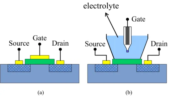
Fig. 2-1 Schematic representation of (a) MOSFET, (b) ISFET
(a) (b)
Fig. 2-2 Series combination of the (a) initial (b) hydrated insulator capacitance
Silicon
Thermal Oxide
Solution
Hydration
U U,
ε
x
x
Ux
HL(t),
ε
USensing Layer
−
HL HL(t),
ε
x
L L,
ε
x
L L,
ε
x
(a) (b) (c) (d) (e) (f)
(g)
(h)
(i)
Fig. 3-1 Fabrication process flow
Fig. 3-2 Measurement setup
Gate
Drain1
Source
Drain2
V
GSFig. 3-3 Detection principle of pH
(a) (b)
(c) (d)
(e)
(a) (b)
(c) (d)
(e)
(a) (b)
(c) (d)
Fig. 4-3 Sensitivities of ISFET and REFET with xU=100Å, W/L=400μm/40μm. (e)
(a) (b)
(c) (d)
(e)
(a) (b)
(c) (d)
(e)
(a) (b)
(c) (d)
(e)
(a) (b)
(c) (d)
(e)
(a) (b)
(c) (d)
(e)
(a) (b)
(c)
(e)
Fig. 4-9 Sensitivities of ISFET and REFET with xU=500Å, W/L=400μm/40μm. (d)
(a) (b)
(c) (d)
(e)
g. 4-10 Sensitivities of ISFET and REFET with xU=1000Å, W/L=400μm/20μm. Fi
(a) (b)
(c)
(e)
Fig. 4-11 Sensitivities of ISFET and REFET with xU=1000Å, W/L=400μm/30μm. (d)
(a) (
(e)
Fig. 4-12 Sensitivities of ISFET and REFET with xU=1000Å, W/L=400μm/40μm. b)
Sensitivity pH 1-13 ( SiO2 / Ta2O5) Sensitivity pH 1-13 ( △V ) Sensitivity pH 1-9 ( △VG ) Sensitivity pH 9-13 ( △VG ) G SiO2 (100Å) W/L = 400/20 30.95 / 53.71 23.17 21.53 27.1 SiO2 (100Å) W/L = 400/30 27.82 / 54.9 27.08 22.11 38.17 SiO2 (100Å) W/L = 400/40 33.39 / 56.21 22.83 18.92 32.88 SiO2 (300Å) W/L = 400/20 28.25 / 55.23 26.98 20.35 41.64 SiO2 (300Å) W/L = 400/30 22.08 / 53.66 31.58 27.87 41.3 SiO2 (300Å) W/L = 400/40 35.01 / 55.02 20.02 14.6 34.65 SiO2 (500Å) W/L = 400/20 36.76 / 55.66 18.9 15.65 27.61 SiO2 (500Å) W/L = 400/30 28.2 / 54.72 26.53 24.01 36.67 SiO2 (500Å) W/L = 400/40 32.88 / 55.49 22.61 17.17 36.56 SiO2 (1000Å) W/L = 400/20 30.96 / 54.15 23.19 20.15 31.56 SiO2 (1000Å) W/L = 400/30 37.04 / 55.12 18.08 13.55 30.69 SiO2 (1000Å) W/L = 400/40 30.62 / 50.86 20.24 17.97 25.73
T an ses to trolyte. △ he difference between
ISFET and REFET gate voltages. able 4-1 SiO2 d Ta2O5 respon pH elec VG is t
Fig. 4-13 Drift ch iO2-gate ISFET.
Fig. 4-14 Drift characteristics of the 300Å PECVD SiO2-gate ISFET.
Fig. 4-15 Drift characteristics of the 500Å PECVD SiO2-gate ISFET.
Fig. 4-17 Average drift of the PECVD SiO2-gate ISFET during the last 5 hour.
100Å PECVD SiO2 300Å PECVD SiO2 500Å PECVD SiO2 1000Å PECVD SiO2 300Å Sputtered Ta2O5 Average Gate-Voltage Drift (mV/hour) 7.4 12.8 15.4 16.2 1.6
Fig. 4-19 ID-VG curve of the 100Å SiO2-gate ISFET.
Fig. 4-21 ID-VG curve of the 500Å SiO2-gate ISFET.