© 2005 The Electrochemical Society. 关DOI: 10.1149/1.2138671兴 All rights reserved. Manuscript submitted May 26, 2005; revised manuscript received September 15, 2005. Available electronically December 23, 2005.
Thermal oxides grown on n+-doped polysilicon 共polyoxides兲 have been widely used in nonvolatile memories such as EPROM, EEPROM, and flash EEPROM cells.1-4Of particular importance in most applications is that the polyoxides exhibit a low leakage cur-rent and a high breakdown field. The breakdown strength is strongly influenced by the smoothness of the polyoxide/polysilicon interface.5,6According to previous studies,7-9the electrical proper-ties of the polyoxides have been shown to depend on the polysilicon deposition temperature, doping process, and oxidation temperature. Also, the difference in the degree of roughness at the top and bottom interfaces causes the bias-polarity dependence of the current-field characteristics. In order to obtain good data retention characteristics, the polyoxide with low conductivity and high breakdown fields have long been sought.10-13 More importantly, some floating-gate non-volatile memories that rely on electron tunneling through the poly-oxides require a high charge to breakdown共Qbd兲 and low trapping rate during programming and erasing operations.14
It was reported that more reliable dielectrics could be grown on polysilicon by using deposited instead of thermally grown polyox-ides. For those chemical vapor deposited 共CVD兲 dielectrics, the grain boundaries present in the bottom polysilicon are not incorpo-rated in the deposited layer due to no polysilicon consumption. The surface of the polysilicon layer is not roughened, so the CVD oxide potentially has a defect density relatively independent of the bottom polysilicon.15-18
N2O used as an oxidant or a postoxidation annealing ambient for the gate dielectrics grown on single-crystal Si has received much attention due to its endurance to Fowler-Nordheim共F-N兲 stress. This is attributed to the incorporation of nitrogen at the oxide/silicon– substrate interface.19,20 It has been shown that N2O-grown oxide exhibits reduced electron trappings, superior breakdown properties, and suppressed interface state generation under the hot-carrier stress, as compared to pure SiO2.21Recently, N2O was applied to grow polyoxide on n+-polysilicon in the oxidation furnace22to ob-tain polyoxide of better integrity, also due to incorporation of nitro-gen in polysilicon grain boundaries to form oxynitride. The oxyni-tride formed reduces the enhanced oxidation effect of grain boundaries to make the polyoxide/poly-1 interface smoother.
In this paper, we applied the N2O oxidation to n+doped polysili-con to grow polyoxides by using rapid thermal processing共RTP兲 and studied the electrical characteristics of the grown polyoxides. The study was in terms of the oxidation temperature and thickness with O2oxidation samples as comparison. Atomic force microscopy
共AFM兲, transmission electron spectroscopy 共TEM兲, and secondary ion mass spectroscopy共SIMS兲 measurements were employed to cor-relate electrical characteristics with the physical structures. Results showed that N2O samples exhibited better characteristics than O2-grown samples; however, as the oxidation temperature was in-creased, the electrical characteristics of N2O samples became de-graded, even though they still showed superior characteristics than the O2-grown samples. Also, the hole-trapping phenomenon was observed in the N2O-grown polyoxides. In addition, the two-step RTP oxidation, i.e., first RTP oxidizing the polysilicon in O2then in N2O, was studied. Improved characteristics were obtained. With all the experimental data, it is concluded that to obtain improved char-acteristics by using the N2O rapid thermal oxidation, only an appro-priate amount of nitrogen should be incorporated.
Experimental
In this study, n+-polysilicon/polyoxide/n+-polysilicon capacitors were fabricated. At first, p-type wafers were thermally oxidized to have a field oxide of a thickness of 100 nm. All samples were then deposited on a 300-nm polysilicon film at 620°C and doped with POCl3 at 875°C. The sheet resistance of the film was 85⍀/䊐. Then, interpolyoxides with a thickness of the range 85–200 Å were grown on the polysilicon films at 950–1050°C for time ranging from 50 to 500 s in a pure N2O ambient by using an AG610 RTP processor. For comparison, polyoxides with a thickness of 115 Å were grown at 950 and 1050°C for 180 and 50 s, respectively, in a pure O2ambient, also by RTP. The flow rate for N2O and O2was all 3 slm. In order to study the N2O annealing effect, samples were first oxidized with RTP at 950°C for 180 s in the pure O2ambient and then annealed in the N2O ambient at 950°C for 90 s with RTP. The final thickness of the oxide was about 155 Å. After the interpolyox-ide formation, a second polysilicon film共poly-2兲 of about 300 nm was deposited which was doped by POCl3to a sheet resistance of 85⍀/䊐. After poly2 was patterned, all samples were grown on a 100-nm-thick oxide via wet oxidation at 850°C. Contact holes were opened and metallized to form the capacitor structure. Finally, all devices were sintered at 350°C for 40 min in the N2gas, which can improve the metallurgy between polysilicon and metal film with reduced resistance.
Polyoxide thickness was determined by the high-frequency 共1 MHz兲 using Keithley capacitance-voltage 共C-V兲 measurements. The morphology of the polyoxide/polysilicon interface was studied by TEM and AFM. For the AFM measurement of the surface, to reveal the polyoxide/poly-1 interface, the polyoxide layer was re-moved by wet etching in the buffered HF acid. The true replica of the interface may be preserved by such a treatment because the z
poly-Si is not attacked by the HF-based solution.23 The current-voltage共I-V兲 characteristics were measured by using an HP4145B semiconductor parameter analyzer.
Results and Discussion
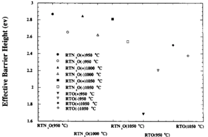
Figure 1a and b shows the typical positive and negative J-E characteristics of the N2O-grown and O2-grown polyoxides with the thickness of 115 Å grown at the temperature of 950, 1000, and 1050°C, respectively. It can be seen that the N2O-grown polyoxides conducted a lower leakage current and a higher breakdown electric field than those of the O2-grown polyoxides for both the positive and negative gate biases. For the O2-grown polyoxides, the J-E char-acteristics were improved for the higher growth temperature. How-ever, for the N2O-grown polyoxides, the dielectric breakdown field 共Ebd兲 degraded as the growth temperatures increased. For both poly-oxides, the positive characteristics were better than the negative characteristics. Shown in Fig. 2 is the derived values of the effective barrier height,b, of the O2-grown polyoxide and N2O-grown poly-oxide where the effective electron mass within the polypoly-oxide band-gap has been taken as 0.5 m0共m0: free electron mass兲. As expected, the barrier heights of the N2O-grown polyoxides were all higher than those of the O2-grown polyoxides. This indicates that the N2O-grown polyoxides had smoother poly-1/polyoxide surfaces than those of the O2-grown polyoxides. Furthermore, for the N2O-grown polyoxide, the barrier heights of the positive character-istics 共injection from the polyoxide/poly-1 interface兲 were better than those of the negative characteristics共injection from the poly-2/ polyoxide interface兲. This seems to indicate that the bottom poly-1/ polyoxide interface is smoother than the top poly-2/polyoxide inter-face for the N2O-grown polyoxide. However, for the O2-grown
polyoxides, their barrier heights were improved for the higher oxi-dation temperature, which may be due to smoother interface at the higher oxidation temperature of 1050°C. For the N2O-grown poly-oxides, their barrier heights slightly degraded for the higher growth temperature. The above J-E characteristics may be related with the morphology of the polyoxide/polysilicon interfaces.
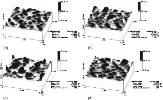
In order to investigate the actual morphology of the interface between the polyoxide and polysilicon, AFM measurements were performed for the polyoxides. Figure 3a and b shows the AFM im-ages of the surfaces of the N2O-grown polyoxides grown at tem-peratures of 950 and 1050°C, and the average roughness共Ra兲 val-ues of AFM are 35.8, and 37.2 Å, respectively. Figure 3c and d shows the same pictures for the O2-grown polyoxides grown at the same temperatures of 950 and 1050°C, and the average roughness 共Ra兲 values of AFM are 51 and 39.6 Å, respectively. It can be seen that the N2O-grown polyoxides with lower Ra values had smoother poly-1/polyoxide surfaces than those of the O2-grown polyoxides. This smoother surface of the N2O-grown polyoxide can be attrib-uted to the nitrogen diffusing into grain boundaries and reducing the grain boundary enhancement effect. Furthermore, for the N2O-grown samples, the 950°C sample had a slightly smoother in-terface than that of the 1050°C sample, which may be due to exces-sive nitrogen during higher oxidation temperature incorporated into polyoxide/polysilicon interface to induce larger thickness nonuniformity24across the wafer, despite a locally smoother surface. For the O2-grown samples, the 1050°C sample had a smoother in-terface than that of the 950°C sample due to operating of viscous flow of SiO2 and polysilicon, and diffusion controlled at higher oxidation temperature. Cross-sectional TEM micrographs were also taken for the above samples. They are shown in Fig. 4a and b for the 950 and 1050°C N2O-grown samples, respectively, and in 4c and d for the 950 and 1050°C O2-grown samples, respectively. We can see that the N2O-grown polyoxides had larger grain sizes on the poly-1 and smoother polyoxide/poly-1 interfaces than those of the O2-grown polyoxides. Furthermore, for the N2O-grown polyoxides, the bottom poly-1 film had more uniform distribution and larger grain sizes than those of the top poly-2 film. This seems to indicate the bottom 1/polyoxide interface is smoother than the top poly-2/polyoxide interface as barrier height revealed. However, for the N2O-grown polyoxides, the 950°C sample had a slightly smoother polyoxide/polysilicon interface than that of the 1050°C sample共see Fig. 4a and b兲. For the O2-grown polyoxides, the 1050°C sample had a smoother polyoxide/polysilicon interface than that of the 950°C sample共see Fig. 4c and d兲.
The slightly smoother surfaces of the N2O-grown polyoxides can be attributed to the nitrogen, which diffused along and into grain boundaries of the polysilicon to form oxynitride at grain boundaries,
Figure 1. J-E characteristics of the N2O-grown and O2-grown polyoxides of
a thickness of 115 Å grown at 950, 1000, and 1050°C for the top gate applied at共a兲 a positive and 共b兲 negative bias, respectively.
Figure 2. Effective barrier height, b, of the N2O-grown and O2-grown
and the oxynitride reduced the enhanced oxidation effect of grain boundaries.25However, too much nitrogen induces larger thickness nonuniformity across the wafer, despite a locally smoother surface. Figure 5 shows the thickness distributions of polyoxides parallel to the wafer flat surface from the center to the two edges for the O2-grown and N2O-grown polyoxides, which had nearly the same thickness at the center. It can be seen that the thickness deviation was only 3–4 Å 共3%兲 for the O2-grown polyoxide but was about 15 Å共13%兲 for the N2O polyoxide grown at 950°C, increasing to 32 Å共27%兲 for the N2O polyoxide grown at 1050°C.
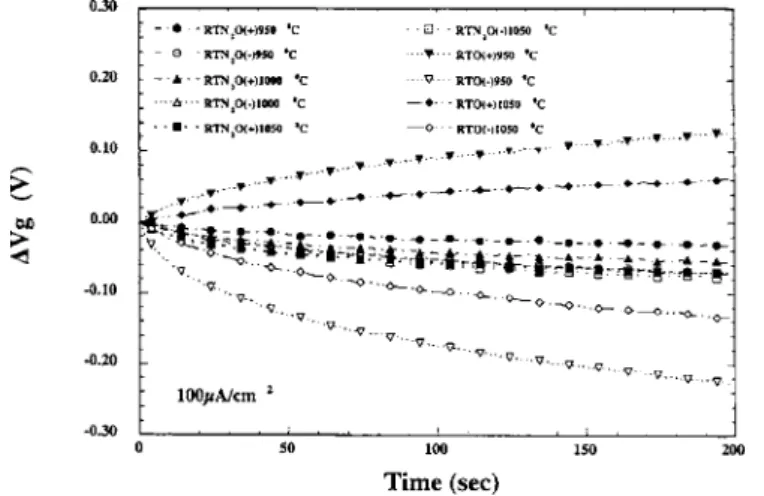
The charge trapping characteristics of the polyoxides were inves-tigated. Figure 6 shows the curves of gate voltage shift共⌬Vg兲 vs
time for both the N2O-grown and the O2-grown polyoxides under a constant ±10 mA/cm2current stress. The area of the test capacitor was 5⫻ 10−4cm2. In the figure, the 950°C O
2-grown polyoxide exhibited the largest electron trapping rates in both polarity stresses. As the temperature increased, the trapping rates decreased. For the N2O-grown polyoxides, it can be seen that initial hole trappings occurred under the positive constant current stress for all the samples and the higher the growth temperature, the larger the hole trapping rate.26For the negative stress, electron trapping rates were lower than those of the O2-grown polyoxides. These results were similar to those found for the oxides grown in N2O and O2mixtures Figure 3. AFM images of the poly1 surfaces of共a兲 the N2O-grown polyoxide at 950°C,共b兲 the N2O-grown polyoxide at 1050°C,共c兲 the O2-grown polyoxide at 950°C, and共d兲 the O2-grown polyoxide at 1050°C.
Figure 4. Cross-sectional TEM micro-graphs of 共a兲 N2O-grown polyoxide at
950°C, 共b兲 N2O-grown polyoxide at
1050°C, 共c兲 O2-grown polyoxide at
950°C, and 共d兲 O2-grown polyoxide at
on single-crystalline silicon by Okada et al.27These were attributed to the nitrogen compilation at the oxide/silicon interface for the N2O oxidation.28Here we also found the same result for the N2O-grown polyoxide for which the SIMS data for nitrogen for the samples are shown in Fig. 2-7. In this figure, the 1050°C N2O-grown sample had the largest nitrogen concentration in the polyoxide, while the 950°C O2-grown sample had the minimal amount of nitrogen con-centration.
In order to speed up oxide breakdown and reduce testing time, the higher constant current stress 10 mA/cm2was selected to apply on the charge-to-breakdown共Qbd兲 test. Figure 8 shows the depen-dence of the charge-to-breakdown Qbd共to 50% cumulative failure兲 under ±10 mA/cm2stress on the oxidation temperature for capaci-tors with N2O and O2-grown polyoxides. Although Qbd for the N2O-grown polyoxide at 950°C is much larger than that for the O2-grown polyoxide, the Qbd for the N2O-grown polyoxide de-creased with the increasing oxidation temperature, whereas that for the O2-grown polyoxide increased gradually. This result is similar to the case for the oxide grown on single-crystal silicon in N2O as reported by Kwong et al.29,30This Qbd decrease was attributed to large undulations at the Si/SiO2interface to induce the large oxide thinning, which was incurred by the excessive nitrogen incorpora-tion at the Si/SiO2 interface during N2O oxidation at higher
tem-peratures, leading to an inhomogeneous oxide growth. This resulted in localized high electric fields leading to smaller Qbd’s.
Figure 9 shows the plots of the electric breakdown field vs the oxide thickness of the range of 85–200 Å for the 950°C N2O-grown polyoxides. The electric breakdown field decreased with the increase in the polyoxide thickness. This may be due to the longer oxidation time, resulting in a rougher bottom polyoxide/polysilicon interface caused by the enhanced oxidation rate at the grain boundaries31 despite the incorporated nitrogen at the polysilicon/polyoxide inter-face. Figure 10 shows the charge trapping characteristics of the 950°C N2O-grown polyoxides of the thickness of 115, 155, and 197 Å, respectively. For the thinner 共115 Å兲 polyoxide, under the positive constant current stress, there were initially small hole trap-pings followed by electron traptrap-pings. This initial hole trapping di-minished as the oxide thickness increased. For the thickest共197 Å兲 polyoxide, there were no initial hole trappings but electron trappings only. As mentioned previously, hole trappings are due to nitrogen piled-up at the polysilicon/polyoxide interface. For the thinner poly-oxide, more nitrogen piled-up at the interface. As polyoxide thick-ness increased, a longer oxidation time resulted in a rougher inter-face, leading to larger electron trappings. The Qbdof these samples depended on their electron trappings. The thinner polyoxide, which
Figure 5. Measured distribution of the polyoxide thickness parallel to the wafer flat surface from the center to the two edges with nearly the same thickness at the center for the N2O-grown and O2-grown polyoxides.
Figure 6. Curves of gate voltage shifts共⌬Vg兲 vs time of the polyoxides of
the N2O-grown and O2-grown polyoxides under ±10 mA/cm2stressing.
Figure 7. SIMS nitrogen profiles of the N2O-grown and O2-grown
polyox-ides grown at 950 and 1050°C.
Figure 8. Charge-to-breakdown Qbd 共50% cumulative failure兲 of the
N2O-grown and O2-grown polyoxides grown at 950–1050°C under
had a lower electron trapping rate, had a larger Qbd; and the thicker polyoxide, which had a higher electron trapping rate, had a smaller Qbd.
In general, the rapid thermal oxidation共RTO兲-grown polyoxide has a higher breakdown field共8–9 MV/cm兲 and reduced leakage current than that grown in the conventional furnace共5–6 MV/cm兲 due to smoother interface by the rapid thermal process.32 Further-more, the RTN2O-grown polyoxide at moderate growth temperature can reach a high breakdown field共13–14 MV/cm兲 and low leakage current due to nitrogen incorporated and existing in the interfaces. But when RTN2O oxidation occurs at higher temperatures, exces-sive nitrogen incorporated at the Si/SiO2interface leads to an inho-mogeneous oxide growth and thickness nonuniformity.
In order to improve the thickness nonuniformity of the N2O-grown polyoxide by RTP, the two-step oxidation, i.e., first RTP oxidizing the polysilicon in O2then RTP oxidizing the polyoxide in N2O, was also investigated.33,34With this two-step oxidation pro-cess, the amount of nitrogen, which was to be incorporated into the polysilicon/polyoxide interface to improve the polyoxide character-istics, could be well controlled by controlling the duration of the RTP N2O oxidation at the second step. Figure 11 shows the positive and negative J-E characteristics of the two-step RTP oxidation poly-oxides at a temperature of 950°C. It can be seen that the grown polyoxide had significant improvements on both their positive and
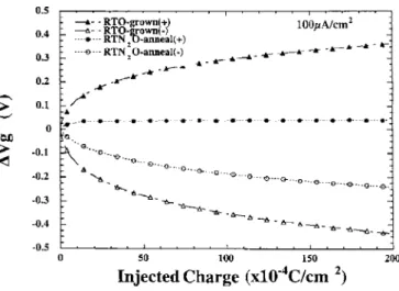
negative characteristics on the leakage current and the Ebdthan the O2-grown polyoxide. In addition, it was also found that the two-step oxidation polyoxide had much improved thickness uniformity, with a thickness deviation of only 5–6 Å共i.e., ⬃5%兲, which was similar to that of the O2-grown polyoxide. Figure 12 shows the charge trap-pings of the two-step oxidation polyoxide with the O2-grown poly-oxide under the ±100A/cm2 stress for comparison. The lower current stress 100A/cm2was used on the charge trapping for the monitors of the locations and amounts of trapped charges. It is seen that the large electron trapping of the O2-grown polyoxide can be suppressed by the second-step N2O oxidation.35,36
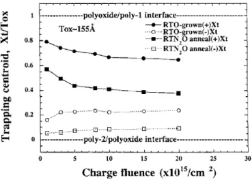
The centroid of trapped charges, Xt, and the trapped charges, as a function of injected charges, of the two-step oxidation polyoxide and the O2-grown polyoxide for the positive and negative constant current injections are shown in Fig. 13 and 14, respectively.37,38In Fig. 13, one can find that Xt of the two-step oxidation polyoxides was further away from the polyoxide/poly-1 interface than that of the O2-grown polyoxide. This may be because the nitrogen incorpo-rated at the polyoxide/poly-1 interface released the stress between the polysilicon and the polyoxide, therefore reducing the potential trapping sites near the polyoxide/poly-1 interface. In Fig. 14, one can see that the trapped charges in the two-step oxidation polyoxide were significantly suppressed as compared to the O2-grown polyox-ide. For the polarity dependence of the trapping characteristics, one sees that the electron-trapped charges were higher under the
nega-Figure 9. Plots of the electric breakdown field vs polyoxide thickness rang-ing from 85 to 200 Å for the N2O-grown polyoxides grown at 950°C.
Figure 10. Charge trapping characteristics of the N2O-grown polyoxides
grown at 950°C having thicknesses of 115, 155, and 197 Å, respectively.
Figure 11. Positive and negative J-E characteristics of the two-step RTP oxidation polyoxides grown at 950°C.
Figure 12. Charge trappings of the O2-grown and N2O-anneal polyoxides
tive injection than the positive injection for the two-step oxidation polyoxide, while lower under the negative injection than the positive injection for the O2-grown polyoxide.
Conclusion
In this paper, we have studied the electrical characteristics of RTP N2O polyoxides in terms of their oxidation temperature and thickness with O2oxidation polyoxides as comparison. AFM, TEM, and SIMS measurements were employed to correlate the electrical characteristics with the physical structures. Results show that RTP N2O-grown polyoxides exhibit better characteristics than O2-grown polyoxides on the leakage current, Ebd, trappings, and Qbd. It is found that it is the nitrogen incorporated into the polyoxide and at the polyoxide/polysilicon interface during the RTP oxidation process which improves the quality of the polyoxide. The nitrogen in N2O improves the interface of the polyoxide/polysilicon, thus improving the characteristics of polyoxides. However, the amount of nitrogen incorporated is critical in determining the quality of the polyoxide. Too much nitrogen does not improve but instead degrades the qual-ity of the polyoxide. This was evidenced by the polyoxides, which were RTP oxidized at higher oxidation temperatures had poorer quality due to too much nitrogen in the oxide as revealed by SIMS data. Too high oxidation temperature共1050°C兲 also causes thick-ness nonuniformity. Also, initial hole trapping phenomenon during
4. N. Mielke, A. Fazio, and H. C. Liou, in Proceedings of the 1987 IEEE/IRPS, pp. 85–92共1987兲.
5. H. L. Peek and J. F. Verwey, Paper 90 presented at The Electrochemical Society Meeting, San Francisco, CA, May 8–13, 1983.
6. P. A. Heimann, S. P. Murarka, and T. T. Sheng, J. Appl. Phys., 53, 6240共1982兲. 7. L. Faraone, R. Vibronek, and J. Mc Ginn, IEEE Trans. Electron Devices, ED-32,
577共1985兲.
8. L. Faraone, IEEE Trans. Electron Devices, ED-33, 1785共1986兲.
9. S. Mori, N. Arai, Y. Kaneko, and K. Yoshikawa, IEEE Trans. Electron Devices,
ED-38, 270共1991兲.
10. C. Cobianu, O. Popa, and D. Dascalu, IEEE Electron Device Lett., 14, 213共1993兲. 11. C. H. Kao, C. S. Lai, and C. L. Lee, IEEE Electron Device Lett., 18, 526共1997兲. 12. C. H. Kao, C. S. Lai, and C. L. Lee, IEEE Trans. Electron Devices, 45, 2238
共1998兲.
13. S. L. Wu, T. Y. Lin, C. L. Lee, and T. F. Lei, IEEE Electron Device Lett., 14, 113 共1994兲.
14. J. H. Klootwijk, H. van Kranenburg, P. H. Woerlee, and H. Wallinga, IEEE Trans.
Electron Devices, 46, 1435共1999兲.
15. J. H. Klootwijk, M. H. H. Weusthof, H. van Kranenburg, P. H. Woerlee, and H. Wallinga, IEEE Electron Device Lett., 17, 358共1996兲.
16. J. H. Klootwijk, H. van Kranenburg, C. Cobianu, V. Petrescu, P. H. Woerlee, and H. Wallinga, in Proceedings of the European Solid-State Device Research Conference, pp. 383–386共1995兲.
17. T. F. Lei, J. Y. Cheng, S. Y. Shiau, T. S. Chiao, and C. S. Lai, IEEE Trans. Electron
Devices, 45, 912共1998兲.
18. P. Candelier, F. Mondon, B. Guillaumont, G. Reimbold, and F. Martin, IEEE
Elec-tron Device Lett., 18, 306共1997兲.
19. Z. Liu, H. J. Wann, P. K. Ko, C. Hu, and Y. C. Chang, Tech. Dig. - Int. Electron
Devices Meet., 1992, 625.
20. H. Hwang, W. Ting, D. L. Kwong, and J. Lee, Tech. Dig. - Int. Electron Devices
Meet., 1990, 421.
21. A. Uchiyama, H. Fukuda, T. Hayashi, and T. Iwabuchi, Tech. Dig. - Int. Electron
Devices Meet., 1990, 425.
22. C. S. Lai, T. F. Lei, and C. L. Lee, IEEE Electron Device Lett., 16, 385共1995兲. 23. M. C. Jun, Y. S. Kim, and M. K. Han, Appl. Phys. Lett., 66, 2206共1995兲. 24. T. Y. Chu, W. T. Ting, J. Ahn, and D. L. Kwong, J. Electrochem. Soc., 138, L13
共1991兲.
25. C. S. Lai, T. F. Lei, and C. L. Lee, IEEE Trans. Electron Devices, 43, 326共1996兲. 26. A. Melik-Martirosian, T. P. Ma, X. W. Wang, X. Guo, F. P. Widdershoven, D. R. Wolters, V. J. D. van der Wal, and M. J. van Duuren, in VLSI Technology, Systems,
and Applications, 2001 International Symposium, April 18–20, 2001, pp. 138–141.
27. Y. Okada, P. J. Tobin, P. Rushbrook, and W. L. Dehart, IEEE Trans. Electron
Devices, 41, 191共1994兲.
28. H. Fukuda, T. Arakawa, and S. Ohno, in Proceedings of the Conference on Solid
State Devices Material, p. 159共1990兲.
29. A. B. Joshi, G. W. Yoon, J. Kim, G. Q. Lo, and D. L. Kwong, IEEE Trans. Electron
Devices, 40, 1437共1993兲.
30. G. W. Yoon, A. B. Joshi, J. Kim, G. Q. Lo, and D. L. Kwong, IEEE Electron
Device Lett., 13, 606共1992兲.
31. S. L. Wu, C. Y. Chen, T. Y. Lin, C. L. Lee, T. F. Lei, and M. S. Liang, IEEE Trans.
Electron Devices, ED-44, 153共1997兲.
32. G. Q. Lo, A. W. Cheung, and D. L. Kwong, Appl. Phys. Lett., 57, 1675共1990兲. 33. H. Hwang, W. Ting, D. L. Kwong, and J. Lee, Tech. Dig. - Int. Electron Devices
Meet., 1990, 421.
34. A. Bhattacharya, C. Vorst, and A. H. Carim, J. Electrochem. Soc., 132, 1900 共1985兲.
35. J. Ahn, W. Ting, T. Chu, S. N. Lin, and D. L. Kwong, J. Electrochem. Soc., 138, L39共1991兲.
36. H. Hwang, W. Ting, B. Maiti, D. L. Kwong, and J. Lee, Appl. Phys. Lett., 57, 1010 共1990兲.
37. Z. H. Liu, P. T. Lai, and Y. C. Cheng, IEEE Trans. Electron Devices, 38, 344 共1991兲.
38. M. S. Liang, N. Radjy, W. Cox, and S. Cagnina, J. Electrochem. Soc., 136, 3786 共1989兲.
Figure 13. Centroids 共Xt兲 of trapped charges of the O2-grown and
N2O-anneal polyoxides under ±100A/cm2injections.
Figure 14. Trapped charges共Qox兲 of the O2-grown and N2O-anneal