Quality improvement of transmission images for transparent displays
with micro-lens array
T.-W. Huang*
a, W.-D. Jeng
b, Y. Ouyang
c, Y.-H. Tsai
d,K.-C. Lee
d, M. Ou-Yang
aa
Department of Electrical and Computer Engineering, National Chiao Tung Univ., Hsin-Chu city
30001, TAIWAN;
bInstitute of Electrical Control Engineering, National Chiao Tung Univ.,
Hsin-Chu city 30001, TAIWAN;
cDepartment of Electrical Engineering, Chang Gung University,
Taoyuan County 33302, Taiwan;
dDisplay Technology Center, Industrial Technology Research
Institute, Hsin-Chu city 30001, TAIWAN.
ABSTRACT
The technology of electrowetting display (EWD) is the most important method for the traditional displays that can work more efficiently. When the voltage drives, the aperture ratio of the ink will reach 75% and the transmittance can reach 60%. Furthermore, the EWD technology has the advantages such as high transmittance, high switching speed, color performance, low power consumption, and etc. They make the advances of technology development for the transparent displays. However, due to the diffraction phenomenon resulted from periodic pixel structures, when the users observe the background object through the transparent display, the transmitted image will be blurred. In this paper, we recognized the problems by the simulation and constructed the optical model first. In order to avoid the diffraction, we use micro lens array to prevent the rays interfere on the micro structure, so that it will not produce the destructive and constructive interference, so the diffraction effect can be reduced. The micro lens array avoid the light touches the outer frame of EWD pixels. The simulations are simulate at different distance, and the distance of diffraction width is condensed to 91% with respect to the origin. In the future, this concept can apply in other transmitted images of transparent displays.
Keywords: Transparent displays, image quality, diffraction, micro lens array
1. INTRODUCTION
The display industry is always the popular high technology industry to be studied. As the development of technology, the display market of television, monitor, cell phone matures recently in liquid crystal display especially (LCD). Other display technology including Active Matrix Organic Light-emitting Diodes (AMOLED), Electro-phoretic Display (EPD), Plasma Display Panel (PDP) has much advanced development in other technology files too. However the traditional display market saturates from 2012. Therefore, in order to enhance the superiority of display products, many new technology are applied to explore a new display market. The technology of the transflective displays is one of the important technology applied into the new potential display market. In recent international conference of display, the concept of transflective displays are proposed into many applications included window display of product, smart window, vehicle display, etc.
The technology of electrowetting display (EWD) is the most important method for the transflective displays that can work more efficiently. EWD contains conductive liquid, electrodes, oil. It can be realized that the phenomenon of electrowetting is from the applied electric field. When the voltage drives, the aperture ratio of the ink will reach 75% and the transmittance can reach 60%. Furthermore, the EWD technology has the advantages such as high transmittance, high switching speed, color performance, low power consumption, and etc. They make the advances of technology development for the transparent displays. Comparisons between EWD and OLED, EWD doesn’t need color filters and can enhance the light utilization efficiency [1-3]. However, the periodic structures of EWD caused the diffraction. Due to the diffraction phenomenon resulted from periodic pixel structures, when the users observe the background object through the transparent display, the transmitted image as Fig. 1 showing will be blurred. The blurred effect is relative to the distant between the object and EWD. [4-5] Therefore, in this paper, we recognized the problems by the simulation and constructed the optical model first. Then the micro lens array is proposed to reduce or eliminate the diffraction effect for the optical performance improvement of transmitted images of transparent displays.
I
(¡x - ndl l
( x¡
dl
Frect
= F
rect
()* S
x- n
co a a aIca
n=-oo x (/
d\1
a=
F{
rect
()} F 1I S(x
-
n-)
= a sinc(afX)
I S(fX
-n
d)
n=-m\
/
n=-mFigure 1. The blurred image is observed after EWD.
2. STRUCTURE AND DIFFRACTION
The pixel of EWD is observed under a microscope as Fig. 2 showing. The pixels are periodic structure and t’s size is 300 m x 300 m. From Fourier Optics [6], we can easy obtain the light distribution of periodic rectangle at the Fourier plane as (1) showing, where d is pitch, a is pixel size, z is the distance between lens, n is the order number, and . The light distribution is product of sinc and delta functions. The sinc function is relative to pixel size, and the delta function is relative to the pitch and the pixel size. The location of first dark fringe of sinc function is , therefore the pixel size controls the first order dark fringe. If we want to concentrate the light to the central peak, we should choose the big pixel size of EWD or expand the aperture of pixel.
Figure 2. The periodic structure of EWD pixels are 300 m x 300 m rectangles.
-0.rro
cytoF1
SiNxSi02
rro
:
Photo resist(TG6104) Dyed Oil
Si02
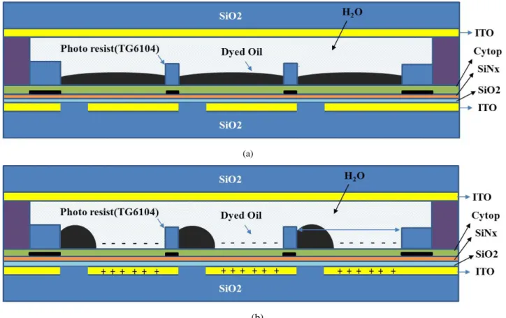
ITO Cytop SiNx SiO2 ITO ' 3. SIMULATIONSThe cross-section drawn of EWD is showing as Fig. 3. The driving voltage of EWD is off in the up figure of Fig. 3, and the driving voltage of EWD is on in the down figure of Fig. 3. When the driving voltage is off, the dyed oil is spread and block the light. When the driving voltage is on, the dyed oil concentrate to the corner and the light can propagate through the pixel. We observed the EWD under a microscope, there are some little dyed oil spread in the bare region as Fig. 4(a) showing. These random little dyed oil will affect the result of simulations if we ignore these random dyed oil.
(a)
(b)
Figure 3. The cross-section drawn of EDW: (a) the driving voltage is off, (b) the driving voltage is on.
(a) (b)
LWll
Di D2
In order to match the real condition, we built the EWD model in optical program, Advanced System Analysis Program (ASAP), with similar random little dyed oil as Fig. 4 (b) showing. The pitch of EWD is 302 m. The interval of delta function are 0.139 mm of measurement and 0.138 mm of simulation, therefore about 1% error between the measurement and the simulation. The interval of sinc function are 2.08 mm of measurement and 2.02 mm of simulation, therefore about 2.9% error between the measurement and the simulation.
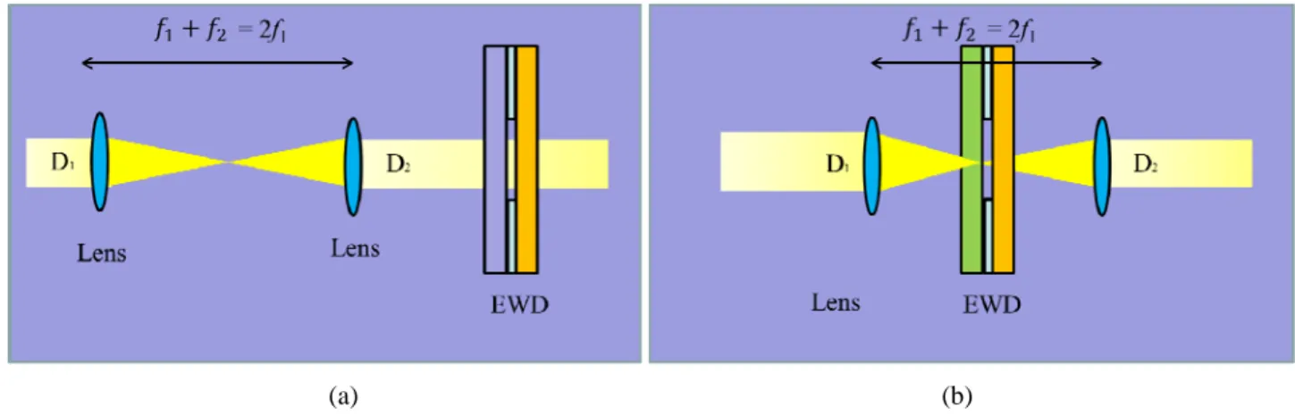
In order to expand the aperture of EWD pixels for reducing diffraction effect, the micro leans array is adopt to avoid that the light is blocked by the outer frame of EDW pixel. As Fig. 5 showing, the micro lens array avoid the light touches the outer frame of EWD pixels. There are two method to add the micro lens array on EWD as Fig. 6 showing. One is that EWD is after the afocal micro lens array as Fig. 6(a) showing, another is that EWD is inserted in the middle of afocal micro lens array as Fig. 6(b) showing.
Figure 5.The micro lens array avoid the light touches the outer frame of EWD pixels.
(a) (b)
Figure 6. (a) EWD is after the afocal micro lens array. (b) EWD is inserted in the middle of afocal micro lens array.
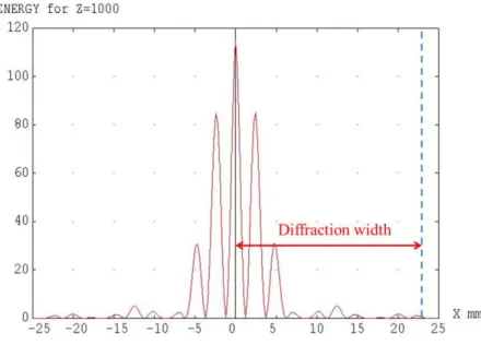
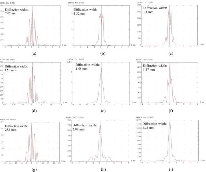
We defined a definition, decreasing percentage of width, to evaluate the diffraction improvement. The decreasing percentage of width is equal to 1-(improved width/original width), where width is half diffraction width as Fig. 7 showing. The light distribution after EWD 30 cm, 50cm, and 1m are simulate with 3 condition as Fig. 8 showing. The light distribution of simulation without micro lens array at 30 cm, 50cm, and 1m are showing in Fig. 8 (a), (b), and (c). The diffraction width of Fig. 8 (a), (b), and (c) are 7.02 mm, 1.32 mm, and 1.1 mm respectively. The light distribution of simulation that EWD is inserted in the micro lens array at 30 cm, 50cm, and 1m are showing in Fig. 8 (d), (e), and (f). The diffraction width of Fig. 8 (d), (e), and (f) are 12.3 mm, 1.58 mm, and 1.47 mm respectively. The light distribution of simulation that EWD is after the micro lens array at 30 cm, 50cm, and 1m are showing in Fig. 8 (g), (h), and (i). The diffraction width of Fig. 8 (g), (h), and (i) are 23.5 mm, 2.98 mm, and 2.21 mm respectively. The decreasing percentages of width in Fig. 8 (a), (b) and Fig. 8 (a), (c) are about 81% and 84%. The decreasing percentages of width in Fig. 8 (d), (e)
ENERGY for Z =1000 120 100- 8060 - 90- 20-0 -25 -20 -15 -10 Diffraction width 10 15 20 25 X mm
and Fig. 8 (d), (f) are about 87% and 88%. The decreasing percentages of width in Fig. 8 (g), (h) and Fig. 8 (g), (i) are about 87% and 91%. It’s clear that the diffraction can be reduced with the micro lens array.
Figure 7. The definition of diffraction width
4. CONCLUSIONS
In this study, the electro-wetting display model is imported into the optical software to simulate the diffraction effect. We proposed that the micro lens array is adopted to reduce diffraction effect for EWD. The micro lens array avoid the light touches the outer frame of EWD pixels. There are two methods to insert the afocal micro lens array. From the simulation after EWD 30 cm, 50 cm, and 1m, it’s clear that the diffraction can be reduced with the micro lens array. The distance of diffraction width is condensed to 91% with respect to the origin. In the future, this concept can apply in other transmitted images of transparent displays.
ACKNOWLEDGEMENT
This paper was particularly supported by the Aim for the Top University Program of the National Chiao Tung University, the Ministry of Education of Taiwan (Contract No. HCH102-39), the National Science Council of Taiwan (Contract No. NSC 102-2220-E-009-016), and Industrial Technology Research Institute of Taiwan. The authors also want to thank them for providing experimental assistance and related information.
REFERENCES
[1] Schultz, A., Heikenfeld, J., Kang, H. S., and Cheng, W., "1000:1 Contrast Ratio Transmissive Electrowetting Displays," Journal of Display Technology 7, 583-585 (2011).
[2] Giraldo, A., Aubert, J., Bergeron, N., Li, F., Slack, A. and Van de Weijer, M., “34.2: Transmissive Electrowetting-Based Displays for Portable Multi-Media Devices,” SID Symposium Digest of Technical Papers 40, 479-482 (2009).
[3] Lao, Y., Sun, B., Zhou, K., and Heikenfeld, J., “Ultra-High Transmission Electrowetting Displays Enabled by Integrated Reflectors,” Journal of Display Technology 4, 120-122 (2008).
[4] Yang, X., L. Wood, T., and Miller, J. H., “Diffraction from Tunable Periodic Structures: Application for the Determination of Electro-Optic Coefficients,” Applied Optics 40, 5583-5587 (2001).
[5] Yang, X., Aspelmeyer, M., Wood, L. T., and Miller, J. H., “Diffraction from Tunable Periodic Structures. II. Experimental Observation of Electric Field-induced Diffraction Peaks,” Applied Optics 41, 5845-5850 (2002).
X mn ENERGY tor 2 =1000 800 700 600 500 400 300 Diffraction width: 2.98 mm 200 100 X mm ENERGY for 2 =300 3000 Diffraction width: 2500. 1.1nun 2000. 1500 1000 -500. II -3 -2 ENERGY for 0 =1000 2000 1800 1600 1900 1200 1000 800 600 900 200 X non ENERGY for 2 =500 1600 1400 1200 1000 800 Diffraction width: 1.47 mm 600 900 200 ¡ 0 -4 -3 -2 -1 X mm ENERGY for Z =1000 120 loo Diffraction width:. i 23.5 mm 00 60 40 20 a 25 -20 -is -lo -s 0 5 10 15 20 25 A . 1 1 ENERGY for a =500 9.013 3 Dlffiachon width: 1.58 aun 0 4 -3 ß -t 0 1 2 3 4 X-ENERGY for Z =500 500 450 400 350 300 250 200 150 100 50 Diffraction width: 12.3 mm 0 n 15 -10 5 Xi 5 10 is ENERGY for Z =700 1400 1200 1000 800 600 400 200 Diffraction width:-7.02 mm-o 8 -4 -2 0 2 4 6 8 Emn
[6] Goodman, J. W., [Introduction to Fourier Optics], 2nd ed., McGraw Hill, New York, 94-125 (2002).
(a) (b) (c)
(d) (e) (f)
(g) (h) (i)
Figure 8. (a), (d), (g): Simulations of EWD without micro lens array after EWD 30 cm, 50cm, and 1m. (b), (e), (h): Simulations, that EWD is inserted in the micro lens array, after EWD 30 cm, 50cm, and 1m. (c), (f),(i): Simulations, that EWD after micro lens array, after EWD 30 cm, 50cm, and 1m.