國 立 交 通 大 學
電信工程研究所
碩士論文
奇偶模雙頻帶通濾波器
Even- and Odd-Mode Dual Band Bandpass Filters
研究生 : 陳如屏
指導教授 : 張志揚 博士
奇偶模雙頻帶通濾波器
Even- and Odd-Mode Dual Band Bandpass Filters
研 究 生 : 陳如屏 Student : Lu-Pin Chen
指導教授 : 張志揚 博士 Advisor : Dr. Chi-Yang Chang
國立交通大學
電信工程研究所
碩士論文
A Thesis
Submitted to Department of Communication Engineering
College of Electrical and Computer Engineering
National Chiao Tung University
In Partial Fulfillment of the Requirements
for the Degree of Master of Science
In
Communication Engineering
July 2009
Hsinchu, Taiwan, Republic of China
i
奇偶模雙頻帶通濾波器
研究生 : 陳如屏 指導教授 : 張志揚 博士
國立交通大學電信工程研究所
摘要
本篇論文提出一個新的雙頻濾波器架構,此濾波器的兩個通帶分別呈現在兩種不 同的輸入訊號下,一種是奇模訊號,另一種是偶模訊號。其中,主要利用耦合微帶 線在針對此兩種訊號輸入時,會有不同波速與特性阻抗的特點,將分別以步階阻抗 諧振器或均勻阻抗諧振器架構設計的兩個帶通濾波器加以組合。並且,適當的控制 微帶線的耦合強度能有效調整兩個通帶的距離。更進一步,利用步階阻抗的諧振特 性,將原本二倍頻的諧振頻率推遠。iii
Even- and Odd-Mode Dual Band Bandpass Filters
Student : Lu-Pin Chen Advisor : Dr. Chi-Yang Chang
Department of Communication Engineering
National Chiao Tung University
Abstract
In this thesis, a new filter structure has two passbands while exciting differential or common signals is proposed. In microstrip coupled lines, there are different characteristic impedances and phase velocities for even- and odd- mode signals. Using the characteristics, the filters can be realized with both stepped-impedance and uniform impedance resonators. By controlling the coupling strength of the coupled lines, the two passbands can be separated effectively. Based on the resonant characteristics of a stepped-impedance resonator, the first spurious harmonic can be higher than 2 f0.
v
Acknowledgement
誌 謝
本篇論文的完成,最要感謝的是指導教授張志揚老師在我念研究所這兩年的指 導,不管是在課業、生活與人生規劃上都給予不少有用的建議。研究上,老師總是 親切又熱心的解答問題,給予很多有創意的想法,並且不乏生活上的關心,培養我 能自動自發敦促自己的能力。其樂觀開朗的生活態度也深深影響著實驗室的每個成 員,讓我們的研究生涯能充滿溫馨與歡笑。在此,真的非常感謝老師。同時,感謝 口試委員郭仁財教授、黃瑞彬教授與邱煥凱教授提供的寶貴建議,使本篇論文更臻 完善。 感謝實驗室學長們無私地指導,幫忙解決在研究上遇到的問題。金雄學長總是 不厭其煩並且有耐心的接我求救電話,遇到研究上的瓶頸時,也時時鼓勵我,讓人 感念在心,無厘頭的人生建言也讓研究生活充滿樂趣。此外,哲慶學長在研究上總 是非常熱心地給予一針見血的指導,讓這篇論文能更加順利的完成,其對研究的熱 忱與努力更是我所要學習的。感謝爽朗的正憲學長幫忙解答我不少研究上的問題, 他認真而追求完美的做事態度也讓我印象深刻。有賴眾多學長姐們的幫忙,這篇論 文才能順利完成。 感謝實驗室同學與學弟妹們在學業與生活上的陪伴與照顧,尤其是繼續攻讀博 班的昀緯,總是很有耐心地與我一起討論問題,雖然不能完全了解,卻總是能在討 論中得到一些意外的收穫。感謝忠傑、殿靖、耿宏、姵潔等等學弟妹們,有你們的 存在讓我的研究生活不曾平淡。此外,感謝在求學過程上一路陪伴我的各方好友與 室友們,有你們的陪伴,即使經歷挫折也能勇敢站起來,感謝你們。 最後要感謝的是默默支持的家人們,爸、媽與弟妹。有了你們的支持,讓我能 放心而專注地完成學業,真的非常感謝你們。vii
Table of Contents
Abstract(Chinese) ... i
Abstract ... iii
Acknowledgement ... v
Table of Contents ... vii
List of Figures ... ix
List of Tables ... xv
Chapter 1 Introduction ... 1
Chapter 2 Basic Theory ... 5
2.1 Analysis and Characteristics of SIR ... 5
2.1.1 Resonance condition and resonator electrical length ... 5
2.1.2 Basic structure of the Half-wavelength Type SIR ... 8
2.1.3 Spurious Resonance Frequency ... 10
2.2 Lowpass Prototype Circuit and the transformation from lowpass prototype to bandpass filter ... 13
2.2.1 The Lowpass Prototype ... 14
2.2.2 Transformation of elements by J- or K-inverter ... 15
2.2.3 Lowpass to Bandpass Transformation ... 18
2.2.4 Slope Parameters ... 19
2.3 Dishal’s Method ... 21
2.4 Coupled Line Theory ... 23
2.4.1 even-and odd- mode approach[17] ... 24
2.5 J- and K-inverters with distributed circuits ... 27
2.5.1 Equivalent Circuit of Parallel-Coupled Line ... 27
viii
2.6 Second-Order Gap Coupling Bandpass Filter ... 34
Chapter 3 Second-Order Tapped Coupling Bandpass Filter ... 41
3.1 Input/Output Tapping ... 41
3.2 Second-Order Bandpass Filter with Tapped Line ... 47
3.3 Dual- Frequency Transformer[19] ... 49
Chapter 4 The Proposed Dual-Band Bandpass Filter ... 51
4.1 Design Procedure and Realization with Type I tapping ... 51
4.1.1 Second-Order Filter with Open-Endedλ/2 SIR ... 51
4.1.2 Second-Order Filter with Short-Ended λ/2 SIR ... 58
4.1.3 Third-Order Filter with Short-Ended λ/2 SIR ... 63
4.2 Design Procedure and Realization with Type II tapping ... 70
4.2.1 Third-Order Filter with Short-Ended λ/2 SIR ... 70
4.3 Design Procedure and Realization with Type III tapping ... 75
4.3.1 Third-Order Filter with Open-Ended λ/2 SIR ... 75
4.3.2 Second-Order Filter with Open-Ended λ/2 SIR ... 85
Chapter 5 Conclusion ... 92
ix
List of Figures
Figure 1.1 The general scheme of a diplexer. ... 2 Figure 1.2 The diplexer structures in a balanced transceiver system. (a) The original
Structure. (b) The modified structure with the proposed even and odd-mode bandpass filter. ... 3 Figure 1.3 The structures of a two channel system in a balanced receiver. (a) The
general structure. (b) The modified structure with the proposed even and odd-mode bandpass filter. ... 4 Figure2.1 Basic structure of SIR. (a) Quarter-wavelength type. (b) Half-wavelength
type. ... 6 Figure 2.2 Electrical parameters of fundamental building element of a SIR. ... 6 Figure 2.3 Resonance condition of SIR. ... 8 Figure 2.4 Basic structure of λ/2-type open-end SIRs. (a) R<1. (b) R=1. (c) R>1. ... 9
Figure 2.5 Basic structure of λ/2-type short-end SIRs. (a) R<1.(b) R=1. (c) R>1. ... 10
Figure 2.6 The relationship between impedance ratio and normalized spurious
resonance frequencies ... 12 Figure 2.7 Normalized resonant frequencies of an SIR. ... 13 Figure 2.8 Lowpass prototype ladder networks. (a) The leading component is a shunt
capacitor; (b) The dual of the network in (a). ... 14 Figure 2. 9 Admittance and impedance inverters ... 15 Figure2.10 The transformation between series and shunt components. (a)
x
to series components. ... 16
Figure 2.11 Transformation of J inverter. ... 16
Figure 2.12 The series inductors can be transformed to shunt capacitor. ... 18
Figure 2.13 Lowpass to bandpass transformation. ... 19
Figure 2.14 Parallel resonances are represented with slope parameters. ... 20
Figure 2.15 Parameters Qex and coupling coefficients k. ... 21
Figure 2.16 Analysis of coupled microstrip lines in terms of capacitances: (a) even-mode capacitance. (b) odd-mode capacitance. ... 25
Figure 2.17 An unsymmetrical pair of parallel-coupled lines. C ,a C and b C are line ab capacitances per unit length. ... 28
Figure 2.18 An unsymmetrical parallel-coupled line and its equivalent circuit. ... 28
Figure 2.19 A symmetrical parallel-coupled line and its equivalent circuit. ... 29
Figure 2.20 An unsymmetrical parallel-coupled line and its equivalent circuit. ... 30
Figure 2.21 A symmetrical parallel-coupled line and its equivalent circuit. ... 30
Figure 2.22 An unsymmetrical parallel-coupled line and its equivalent circuit. ... 32
Figure 2.23 A symmetrical parallel-coupled line and its equivalent circuit. ... 32
Figure 2.24 An unsymmetrical antiparallel-coupled line and its equivalent circuit. ... 33
Figure 2.25 A symmetrical antiparallel-coupled line and its equivalent circuit. ... 33
Figure 2.26 Circuit configuration of the second-order gap coupling filter. ... 34
Figure 2.27 The overall equivalent circuit of the second-order gap coupling filter. ... 35
Figure 2.28 Circuit configuration of the second-order gap coupling filter. ... 37
Figure 2.29 The overall equivalent circuit of the second-order gap coupling filter. ... 37
Figure 3.1 The stepped-impedance resonator and tapped line . ... 42
Figure 3.2 The short-end type SIR and tapped line . ... 44
Figure 3.3 The general case of tapping with SIR. ... 45
xi
Figure 3.5 The SIR feeding structure with a matching network... 46 Figure 3.6 The overall equivalent circuit of the second-order tapped coupling filter. .. 47 Figure 3.7 Circuit configuration of the second-order tapped coupling filter. (Type III) 48 Figure 3.8 The circuit simulation result. ... 48 Figure 3.9 Circuit configuration of the second-order tapped coupling filter. (Type IV) 49 Figure 3.10 Two-section dual-band transformer. ... 50 Figure 4.1 The overall circuit diagram. (a) In circuit simulation tool, ADS. (b) In EM
simulation tool, Sonnet. ... 52 Figure 4.2 The circuit layout of the proposed Filter A. ... 54 Figure 4.3 Photograph of Filter A ... 55 Figure 4.4 Simulated and measured results of Filter A. (a) Simulated S11 and S21
for 2~4 GHz. (b) Simulated S11 and S21 for 1~7 GHz. (c) Measured
11
S and S21 for 2~4 GHz. (d) Measured S11 and S21 for 1~7 GHz. (e) Measured isolation between two modes. ... 58 Figure 4.5 The overall circuit scheme of Filter B. (a) The circuit structure in ADS. (b)
The circuit layout in Sonnet. ... 58 Figure 4.6 Photograph of Filter B. ... 60 Figure 4.7 Simulated and measured results of Filter B. (a) Simulated S11 and S21
for 2~4 GHz. (b) Simulated S11 and S21 for 1~7 GHz. (c) Measured
11
S and S21 for 2~4 GHz. (d) Measured S11 and S21 for 1~7 GHz. (e) Measured isolation between two modes. ... 63 Figure 4.8 The overall circuit configuration of Filter C. (a) The overall layout. (b) The
part of resonators. (c) The part of transformers. ... 65 Figure 4.9 Photograph of Filter C. ... 66
xii
Figure 4.10 Simulated and measured results of Filter C (a) Simulated S11 and S21 for 2~4 GHz. (b) Simulated S11 and S21 for 1~7 GHz. (c) Measured
11
S and S21 for 2~4 GHz. (d) Measured S11 and S21 for 1~7 GHz. (e) Measured isolation between two modes... 69 Figure 4.11 The overall circuit topology of Filter D. ... 70 Figure 4.12 Photograph of Filter D. ... 71 Figure 4.13 Simulated and measured results of Filter D. (a) Simulated S11 and S21
for 2~4 GHz. (b) Simulated S11 and S21 for 1~7 GHz. (c) Measured
11
S and S21 for 2~4 GHz. (d) Measured S11 and S21 for 1~7 GHz.
(e) Measured isolation between two modes... 74 Figure 4.14 The overall circuit topology of the Filter E. (a) The circuit scheme in ADS.
(b) The circuit scheme in Sonnet. ... 76 Figure 4.15 Photograph of proposed Filter E. ... 79 Figure 4.16 Photograph of proposed Filter F. ... 79 Figure 4.17 Simulated and measured results of Filter E. (a) Simulated S11 and S21
for 2~4 GHz. (b) Simulated S11 and S21 for 1~7 GHz. (c) Measured
11
S and S21 for 2~4 GHz. (d) Measured S11 and S21 for 1~7 GHz. (e) Measured isolation between two modes... 82 Figure 4.18 Simulated and measured results of Filter F. a) Simulated S11 and S21
for 2~4 GHz. (b) Simulated S11 and S21 for 1~7 GHz. (c) Measured
11
S and S21 for 2~4 GHz. (d) Measured S11 and S21 for 1~7 GHz.
xiii
Figure 4.19 The circuit configuration of Filter G. ... 86 Figure 4.20 Photograph of proposed Filter G. ... 88 Figure 4.21 Simulated and measured results of Filter F. (a) Simulated S11 and S21
for 2~4 GHz. (b) Simulated S11 and S21 for 1~7 GHz. (c) Measured
11
S and S21 for 2~4 GHz. (d) Measured S11 and S21 for 1~7 GHz. (e) Measured isolation between two modes... 91 Figure 5.1 The comparison of four circuits. (a) Hairpin-resonator filter. (b) Type I
filter in Seciton 2.6. (c) Type III filter in Section 3.2. (d) Parallel-coupled line resonator filter. (e) Simulated results for S11 and S21. ... 94
xv
List of Tables
Table 2.1 Parameters of coupling coefficients and Qext’s with N=2, Lr=0.1dB. ... 22
Table 2.2 Parameters of coupling coefficients and Qext’s with N=3, Lr=0.1dB ... 22
Table 4.1 Initial parameters for the odd-mode filter in Filter A. ... 53
Table 4.2 Physical dimensions of the proposed Filter A. (Unit: mil) ... 54
Table 4.3 Physical dimensions of the proposed Filter B. (Unit: mil) ... 59
Table 4.4 Initial parameters of the even-mode filter in Filter B. ... 59
Table 4.5 Initial parameters of the even-mode filter in Filter C. ... 64
Table 4.6 Physical dimensions of the proposed Filter C. (Unit: mil) ... 66
Table 4.7 Physical dimensions of the proposed Filter D. (Unit: mil) ... 71
Table 4.8 Physical dimensions of the proposed Filter E. (Unit: mil) ... 76
Table 4.9 Initial parameters of the odd-mode filter in Filter E. ... 77
Table 4.10 Initial parameters of the two-section transformer in Filter E. ... 78
Table 4.11 Physical dimensions of the proposed Filter G. (Unit: mil) ... 87
Table 4.12 Initial parameters of the odd-mode filter in Filter G. ... 87
1
Chapter 1
Introduction
With the rapid expansion and growth of wireless communication systems for military and commercial applications, implementation of microwave and mm-wave systems is increasing dramatically due to their advantages over conventional architectures. Commercial applications of these systems include short-haul line-of-sight transmission links for personal communication networks , wireless cable, wireless local area networks (LANs) and mobile broadband systems.
In modern wireless and mobile communication systems, filters are always playing important and essential roles. Planar filters are particularly popular structures because they can be fabricated using printed circuit technology and are suitable for commercial applications due to their compact size and low-cost integration [1]. Moreover, planar filters using the structures of parallel-coupled and cross-coupled resonators are preferable and extensively used in communication systems because of their high practicality and high performance [2]-[6].
To design a planar filter, it is necessary to select proper resonator types since resonators are basic components of a filter. To reduce the resonator size, several types of resonators such as the U-shaped hairpin resonators [4], the open-loop resonators [5], and the folded open-line resonators [6], [7] have been proposed to design different kinds of bandpass filters. However, all of them are always too large. Among these popular resonators, the most frequently used is the stepped impedance resonator (SIR) because it was originally presented not only to reduce the resonator size, but also to control the spurious resonant frequencies by properly adjusting its structural parameters [8],[9].
2
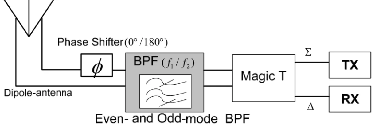
In multiservice and multiband communications, diplexers are one of the key components in the transceiver. They are often needed to have some capabilities of high compactness, light weight, and high isolation. Microwave diplexers are typically employed to connect the RX and TX filters of a transceiver to a single antenna through a suitable three-port junction. Basically, a diplexer is composed of bandpass filters and associated matching networks. Thus, a reduction of the filter size is essential in reducing the size of a diplexer. To reduce the circuit size, the diplexers based on the slow-wave open-loop resonators with high-impedance resonators[6], the folded coupled-line resonators [7], the miniaturized open-loop resonators [8], and stepped-impedance resonators [9] were proposed. However, all of them required two filters in realizing the diplexer. Figure 1.1 shows the general structure of a diplexer.
Figure 1.1 The general scheme of a diplexer.
1
f
2
f
3 Σ ∆ 1 2 ( / )f f
φ
(0 /180 )° °(b) Modified architecture of the diplexer in a balanced transceiver.
Figure 1.2 The diplexer structures in a balanced transceiver system. (a) The original Structure. (b) The modified structure with the proposed even and odd-mode bandpass filter.
Moreover, consider the importance of balanced circuits in modern communication system. It’s necessary to figure out a solution to decrease the circuit size in the balanced transceiver as shown in Figure 1.2(a).
In this thesis, a new four-port bandpass filter is proposed. Unlike the operation of the four-port balanced-to-balanced bandpass filter in [10], the proposed bandpass filter based on SIRs can operate at two different passbands while exciting differential- or common-mode signal respectively. This filter can be used to develop a compact microstrip diplexer by adding additional passive components, e.g. a 0o/180o phase shifter and a magic T, as illustrated in Figure 1.2(b). With the number of filters reduced by half, the size of the proposed diplexer may be made compact when compared with that of the conventional diplexer consisting of two single-passband filters.
On the other hand, another application is for a two-channel system. For example, Figure 1.3(a) depicts a conventional two-channel balanced system. Using the proposed filter design, the number of filters can be reduced by half as presented in Figure 1.3(b). The two channels are selected with the switch of two kinds of phase delay.
4
1
f
2
f
(a) The general structure of a two-channel system in a balanced receiver.
φ
( / )f1 f2(0 /180 )° °
φ
(0 /180 )° °
(b) The modified structure of a two-channel system in a balanced receiver.
Figure 1.3 The structures of a two channel system in a balanced receiver. (a) The general structure. (b) The modified structure with the proposed even and odd-mode bandpass filter.
5
Chapter 2
Basic Theory
2.1 Analysis and Characteristics of SIR
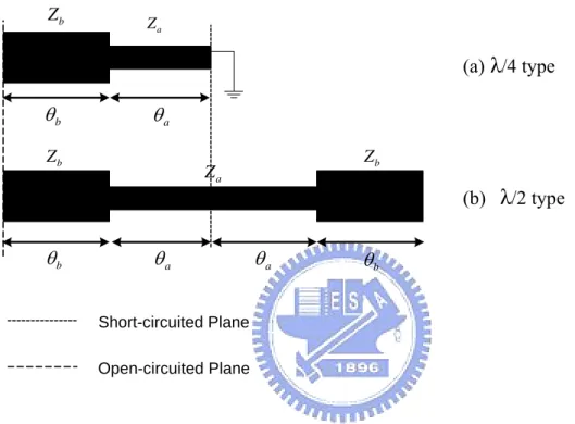
Because we want to fabricate a bandpass filter with SIR and UIR, the basic structure of
λ
/4- andλ
/2-type SIR are presented in this part [11], followed by the introduction and definition of the impedance ratio R. In addition, basic properties such as resonant conditions, resonator length, and spurious resonance frequencies are systematically discussed using R .2.1.1 Resonance condition and resonator electrical
length
The SIR is a TEM or quasi-TEM mode resonator composed of more than two transmission lines with different characteristic impedance. Figure 2.1 shows typical examples of its structural variation, where figures (a) and (b) are examples of
λ
/4 andλ
/2 resonators.Characteristic impedance and corresponding electrical length of the transmission lines between the open- and short-circuited ends in Figure 2.1 are defined as Za and Zb,
a
θ and θb, respectively. The structural fundamental building element of a SIR comprises a composite transmission line possessing both open- and short-circuited ends and a step
6
junction in between. After defining this fundamental building element,
λ
/4- andλ
/2-type of SIR can be looked as a combination of one and two fundamental building elements respectively. An electrical parameter which characterizes the SIR is the ratio of the two transmission line impedances Za and Zb, which we define by the following equation.b a Z R Z ≡ (2.1) (a)
λ
/4 type (b)λ
/2 typeFigure2.1 Basic structure of SIR. (a) Quarter-wavelength type. (b) Half-wavelength type.
Figure 2.2 Electrical parameters of fundamental building element of a SIR.
Figure 2.2 shows the fundamental building element of a SIR with an open-end, short-end and an impedance step. When ignoring the influences of step discontinuity and
a θ b θ b Z a Z i Z ( 1/ )= Yi a θ b θ b Z a Z a θ b θ b Z a Z Zb a θ θb Short-circuited Plane Open-circuited Plane
7
edge capacitance at the open end, the input impedance and admittance defined as Zi and
i Y(=1/Zi) can be expressed as tan tan tan tan a a b b i b b a a b Z Z Z jZ Z Z θ θ θ θ + = − (2.2) Let Yi =0, and then the parallel resonance can be obtained as follows:
tan tan b a b a Z R Z θ θ = ≡ (2.3) Define the overall electrical length of the SIR as θ . With (2.3), T θ can be expressed as TA
TA a b θ =θ +θ 1 tan ( / tan ) a R a θ − θ = + (2.4) Normalized resonator length is defined by the following equation with respect to the electrical length of the corresponding UIR measuring .
/( / 2) 2 /
n TA TA
L =θ π = θ π . (2.5)
Following the resonant condition (2.3), Figure 2.3 shows the relationship between θa
and Ln, taking R as a parameter.
With Figure 2.3, we can choose a curve which represents an impedance ratio R, and then decide the electrical length θa to get a specific Ln which means the overall electrical
length of the SIR is:
( / 2) TA Ln
θ = × π . (2.6) Similarly, for λ - and λ -type SIR, overall electrical lengths are defined as / 2 θ TB
and θTC which can be normalized as follows:
/ 2 / TB TA Ln θ π = θ π = , (2.7) / 2 4 / TC TA Ln θ π = θ π = . (2.8) Figure 2.3 shows that when
(1) R> , the total electrical length of the resonator is longer than 1 λ/ 4 and a maximum value exists.
8 ofthe resonator equals λ . / 4
(3) R< , the total electrical length of the resonator is shorter than 1 λ/ 4 and a minimum value exists.
That is, applying a smaller impedance ratio R and choosing the electrical length properly, the resonator length can be shortened effectively.
Figure 2.3 Resonance condition of SIR.
2.1.2 Basic structure of the Half-wavelength Type
SIR
The proposed bandpass filters are mainly composed by
λ
/2-type UIR or SIR. Figure 2.4 shows the open-end type SIR. For the direct analysis, input admittance Yi seen from an open-end is given as2( tan2 tan )(2 tan 2 tan ) (1 tan )(1 tan ) 2(1 ) tan tan
a b b a i b s b a b a R R Y jY jB R R θ θ θ θ θ θ θ θ + − = = − − − + (2.9)
9
Resonance conditions are obtained by taking Yi =0, which is the same as (2.3).
(a) R<1,θT <π
(b) R=1,θT =π
(c) R>1,θT >π
Figure 2.4 Basic structure of λ/2-type open-end SIRs. (a) R<1. (b) R=1. (c) R>1. The slope parameter bs can be obtained from its definition as follows:
0 0 2 s s dB b d ω ω ω ω = = (2.10) where w0 is the angular resonance frequency and Bs is the total susceptance of the
resonator.
In addition, a lower impedance ratio R can obtain a shorter length of SIR which is similar with the
λ
/4-type mentioned in Section 2.1.1.Similarly, for the short-end type shown in Figure 2.5, the resonance condition can be obtained which is identified with (2.3). On the contrary, the higher the impedance ratio R is, the shorter the electrical length can be.
2θa a Z b
θ
bθ
a Z bZ
Z
b bZ
bZ
Za bθ
bθ
bθ
bθ
a θ θa a θ a θ10
(a) R<1,θT >π.
(b) R=1,θT =π.
(c) R>1,θT >π.
Figure 2.5 Basic structure of λ/2-type short-end SIRs. (a) R<1.(b) R=1. (c) R>1.
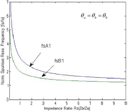
2.1.3 Spurious Resonance Frequency
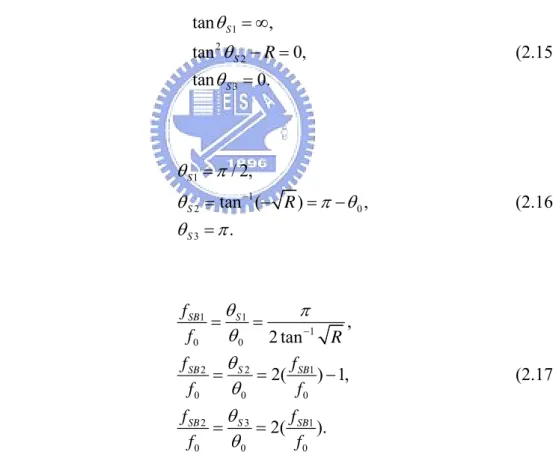
A distinct feature of the SIR is that the resonator length and corresponding spurious resonance frequencies can be adjusted by changing the impedance ratio R [9]. In the
following discussion, the fundamental resonance frequency is represented as f0, while
the lowest spurious frequencies of λ - and / 4 λ -type SIR are represented as / 2 fSA1 and
1 SB
f . Now consider the TEM mode as the dominant resonant mode and neglect the effect
of the step junction. We assume θa =θb =θ0 , and resonator electrical lengths corresponding to spurious frequencies fSA1 and fSB1 are expressed as θSA1 and θSB1.
From (2.3), the following equation is obtained for fSA1.
1 0
tanθSA =tan(π θ− )= −tan− R. (2.11) And then, a θ
θ
a 2θa a Z bθ
aZ
bZ
Z
b bZ
Z
aZ
b bθ
bθ
θ
b bθ
θ
aθ
aθ
b11 1 0 1 0 0 0 1. tan SA SA f f R θ π θ π θ θ − − = = = − (2.12) As previously described , the resonance condition for λ -type SIR can be derived. / 2
In the case of θa =θb =θ0, (2.9) is simplified as [8],
2 0 2 2 4 0 0 2( 1)( tan ) 2(1 ) tan tan i b R R Y jY R R R R θ θ θ + − = − + + + . (2.13) Thus, resonance conditions are expressed as,
1
0 tan R
θ = − . (2.14)
Expressing the spurious resonance frequencies as fSB1, fSB2,fSB3, the corresponding
electrical lengths θ θS1, S2 and θS3 can be obtained from (2.13) as [8],
1 2 2 3 tan , tan 0, tan 0. S S S R θ θ θ = ∞ − = = (2.15) So, 1 1 2 0 3 / 2, tan ( ) , . S S S R θ π θ π θ θ π − = = − = − = (2.16) Thus, 1 1 1 0 0 2 2 1 0 0 0 2 3 1 0 0 0 , 2 tan 2( ) 1, 2( ). SB S SB S SB SB S SB f f R f f f f f f f f θ π θ θ θ θ θ − = = = = − = = (2.17)
Figure 2.6 illustrates the relationship between impedance ratio and normalized spurious resonance frequencies from (2.12) and (2.17a). Figure 2.7 [18] describes the relationship between resonant frequencies including the fundamental, first, second, and third higher order modes against the ratio of electrical lengths for impedance ratio R = 0.2, 0.8, and 2.5. It shows that the smaller the ratio R is, the larger the maximum ratio of
12
0
s
f
f is. It’s a critical characteristic that can be employed for a bandpass filter with a wide
stopband. It’s noted that Figure 2.6 and 2.7 are for the
λ
/2-type SIRs in Figure 2.4. For theλ
/2-type short-end SIRs in Figure 2.5, the same situation holds while the high-Z and the low-Z segments interchange.0
a b
θ
=
θ
=
θ
Figure 2.6 The relationship between impedance ratio and normalized spurious resonance frequencies
13
Figure 2.7 Normalized resonant frequencies of an SIR.
2.2 Lowpass Prototype Circuit and the
transformation from lowpass prototype to
bandpass filter
There are many methods to generate element values for the filter design. The insertion loss method allows a high degree of control of the passband and stopband responses [1]. In our design, the element values for Chebyshev prototypes are used. For the filter prototypes to be discussed below, the order of the filter is equal to the number of reactive elements.
14
2.2.1 The Lowpass Prototype
The lowpass prototype which may be of lumped or distributed realization is a building block from which real filters may be constructed. Various transformations may be used to convert it into a bandpass or other types filter responses with arbitrary centre frequency and bandwidth. The doubly terminated lowpass prototype circuits, connected to their terminating impedances or admittances, are depicted in Figure 2.8. The element values in the network are termed with the “g-parameters” [5], which may be the value of a shunt capacitor or a series inductor. The source termination g0 is resistive if g1 is a capacitor, and conductive if g1 is an inductor, and similarly for the load termination
1 N g + . 0 ( ) s R =g 1( 1) C =g 2( 2) L =g 3( 3) C =g gN+1 (a) 1( 1) L =g 2( 2) L =g 3( 3) L =g 1 N g + 0 ( ) s G =g (b)
Figure 2.8 Lowpass prototype ladder networks. (a) The leading component is a shunt capacitor; (b) The dual of the network in (a).
The circuits of Figure 2.8 can be considered as the dual of each other, and both will give the same response. When the filter specification is given, the “g parameters” are decided.
15
2.2.2 Transformation of elements by J- or
K-inverter
Simply to say, J and K inverters are admittance and impedance inverters which are similar to the ideal quarter-wavelength transformers shown in Figure 2.9.
(2.18 )
(2.19)
Figure 2. 9 Admittance and impedance inverters
There would be a phase delay of ±90 degrees when the wave passes through the inverters for all frequency. That is, the inverters don’t exist in reality. Figure 2.10 illustrates that with K- or J-inverters, we can transform a series component to a shunt component and transform oppositely as well.
K
0 90 ± L Z in ZJ
0 90 ± L Y in Y 2 in L Z ⋅Z =K 2 in L Y ⋅Y = J16 (a)
(b)
Figure2.10 The transformation between series and shunt components. (a) Transformation of series to shunt components. (b) Transformation of shunt to series components.
In Figure 2.10(a), the input impedance Zin should be identified. Likewise, the
analysis is derived as follows. At first, the J inverter in Figure 2.10(a) can transform the short-circuit termination to an open-circuit as shown in Figure 2.11.
)
(
Y
pZin
17
For the circuit of parallel resonance, Y can be derived as p
2 2 1 o p j Y j C j C L ω ω ω ω ω = − = − (2.20)
And if the circuit in Figure 2.10(a) is of series resonance, we can attain
2 2 1 o s Z j Lω ω ω ′ = − (2.21) where 0 1 1 LC L C ω = =
′ ′ is the center angular frequency. For J=1, the input impedance in Figure 2.11 is
2 1 . p in p in Y Z Y Y J = = = (2.22) The equivalence in Figure 2.10(a) holds. That is,
. in p s Z =Y =Z (2.23) which means 2 2 2 2 1 o 1 o j Cω ω j Lω ω ω ω ′ − = − L′ =C (2.24) Similarly, for Figure 2.10(b),
2 1 . s in s p in Z Y Z Y Z K = = = = (2.25) Thus, L=C′ (2.26) Notice that (2.24) and (2.26) exists only when J=1. When it comes to practical realization, using all shunt or series connected resonators can be more convenient.
18 1 N g + 0 1 g = J01=1 2 C 1( 1) C =L 12 1 J = J23=1 3( 2) C =L 34 1 J = 1 1 N N J − = 4 C CN(=LN) 1 1 NN J + =
Figure 2.12 The series inductors can be transformed to shunt capacitor.
At this stage, the dual-network theorem is applied to add unit inverters to the network to transform the series inductors to shunt capacitors. Assuming N is odd, Figure 2.12 shows the series inductors in Figure 2.8(a) can be transformed to shunt capacitor. From (2.23) and (2.25), indeed, the transformed capacitance would be the same as the inductance before transformation. Now the network is composed of parallel resonant resonators and is known as a lowpass prototype circuit. In addition, these inverters have a one-to-one relationship with the physical coupling elements in the final realized filter structure.
2.2.3 Lowpass to Bandpass Transformation
Now we require a transformation to convert the lowpass prototype into a bandpass filter with arbitrary center frequency and bandwidth. This can be achieved by the following transformation. 0 0 1 W ω ω ω ω ω ′ Ω → − = . (2.27) 0 2 f0,
ω = π × f0 corresponds to the center frequency of the bandpass filter.
2 1
0
W ω ω
ω
−
= is the fractional bandwidth.
19 frequency.
From Figure 2.13, the resulting admittance for one of the parallel resonators should be as follows: For j=1, 2,3...N, 1 . jr jr jr jr Y jB j C j L ω ω = = + (2.28) On the other hand, Figure 2.12 shows that
0 0 1 ' . jr j j jB j C jC W ω ω ω ω ω = = − (2.29)
From (2.28) and (2.29), we acquire
0 0 0 0 , . j j jr jr j j C g C W W W W L C g ω ω ω ω = = = = (2.30)
which is the bandpass transformation for the circuit in Figure 2.8(a).
1 N g + 0 1 g = 2r C 12 1 J = J23=1 3r C 34 1 J = 4r C CNr 1r C 1r L L2r L3r 01 1 J = 4r L LNr 1 1 N N J − = 1 1 NN J + =
Figure 2.13 Lowpass to bandpass transformation.
2.2.4 Slope Parameters
In this part, we introduce the susceptance slope parameter “b” to represent the parallel resonant resonators. The definition is the same as (2.10). As Figure 2.14 depicted, we obtain the admittance inverter parameters presented with the slope parameters,
20
normalized source and load impedances, RS and RL.
L R S R 2r C 12 J J23 3r C 34 J 4r C CNr 1r C 1r L L2r L3r 01 J 4r L LNr 1 N N J − JNN+1 1r b b2r b3r b4r bNr
Figure 2.14 Parallel resonances are represented with slope parameters. The admittance inverter parameters JS are
1 01 0 1 , r S b G J W g g = ⋅ , 1 1 , Nr L N N N N b G J W g g + + = ⋅ for j = 1,2,3…N-1 (2.31) where 1 1 , , S L S L G G R R = = 0 0 0 . 2 jr jr jr w w dB b C d ω ω ω = = = (2.32) Similarly, for any resonator exhibits a series-resonance type, we calculate the reactance slope parameter “x” as the definition
0 0 2 w w dX x d ω ω = = (2.33)
where X is the total reactance of the resonant circuit, and we can obtain the K inverters as follows: 1 01 0 1 , r S x R K W g g = ⋅ 1 , 1 1 , j j j j j j b b J W g g + + + = ⋅ , 1 1 , Nr L N N N N x R K W g g + + = ⋅
21 1 , 1 1 . j j j j j j x x K W g g + + + = ⋅ for j = 1,2,3…N-1 (2.34)
2.3 Dishal’s Method
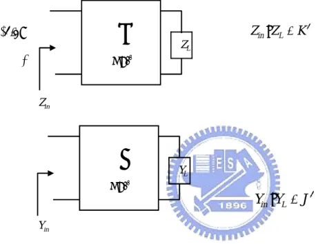
Any narrow-band, lumped-element, or distributed bandpass filter could be described by three fundamental variables: the synchronous tuning frequency of each resonator f0,
the coupling coefficient between adjacent resonators k, and the singly loaded or external Q of the first and last resonators, Qex, as shown in Figure 2.15.
L
R
S
R Qex1 1r k12 k23 k34 kN−1N QexN
b b2r b3r b4r bNr
Figure 2.15 Parameters Qex and coupling coefficients k.
When the bandpass filter specification including fractional bandwidth, maximum insertion loss in the passband are decided, we can derive the required kS and Qexs from
a few simple equations [13].
, 1 , 1 1 1 j j j j jr j r j j J W k b b g g + + + + = = for j=1, 2,3...N− (2.35) 1 1 0 1 1 2 01 , j ex S b g g Q J W G = = (2.36)
22 1 1 2 , 1 . N N N exN N N L b g g Q J W G + + + = = (2.37)
where Wis the fractional bandwidth. Qex1 represents the coupling between RS and the
first resonator whereas QexN is similar but for the last resonator. kj j, +1 corresponds to
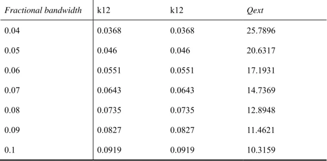
the coupling between the j and th j+1th resonators. For example, Table 2.1 and 2.2 can
be constructed with ripple level 0.1 dB ,
Table 2.1 Parameters of coupling coefficients and Qext’s with N=2, Lr=0.1dB.
Fractional bandwidth k12 Qext
0.04 0.0552 0.069 0.0829 0.0967 0.1105 0.1243 0.1381 21.0767 16.8614 14.0511 12.0438 10.5384 9.3674 8.4307 0.05 0.06 0.07 0.08 0.09 0.1
Table 2.2 Parameters of coupling coefficients and Qext’s with N=3, Lr=0.1dB
Fractional bandwidth k12 k12 Qext
0.04 0.05 0.06 0.07 0.08 0.09 0.1 0.0368 0.046 0.0551 0.0643 0.0735 0.0827 0.0919 0.0368 0.046 0.0551 0.0643 0.0735 0.0827 0.0919 25.7896 20.6317 17.1931 14.7369 12.8948 11.4621 10.3159
23
2.4 Coupled Line Theory
A “coupled line” configuration consists of two transmission lines placed parallel to each other and in close proximity. In such a configuration, there is a continuous coupling between the electromagnetic fields of the two lines. Coupled lines are utilized extensively as basic elements for directional couplers, filters, and a variety of other useful circuits.
Because of the coupling of electromagnetic fields, a pair of coupled lines can support two different modes of propagation. These modes have different characteristic impedances. The velocity of propagation of these two modes is equal when the lines are embedded in a homogeneous dielectric medium (as, for example, in a triplate stripline structure). This is a desirable property for the design of circuits such as directional couplers and filters. However, for transmission lines such as coupled microstrip lines, the dielectric coupled microstrip lines, the dielectric medium is not homogeneous since part of the field extends into the air above the substrate. This fraction is different for the two modes of coupled lines. Consequently, the effective dielectric constants as well as the phase velocities are not equal for two modes. This unequal modal phase velocities may deteriorate the performance of circuits using these types of coupled lines.
When two conductors of a coupled line pair are identical we have a symmetrical configuration. This symmetry is very useful for simplifying the analysis and design of such coupled lines. If the two lines do not have the same impedance, the configuration is called asymmetric.
Coupled transmission lines are usually assumed to operate in the TEM mode, which is rigorously valid for stripline structures and approximately valid for microstrip structures. For that reason, the properties of coupled lines can be determined from the self- and mutual inductors and capacitances for the lines.
24
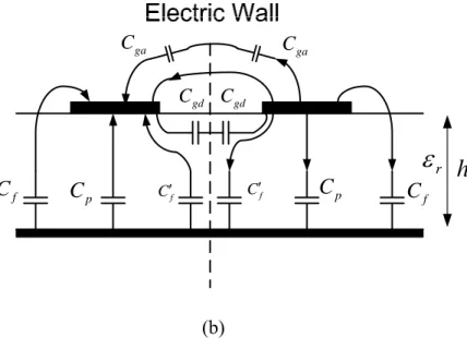
2.4.1 even-and odd- mode approach
[17]Coupled microstrip structures are characterized by the characteristic impedances (or admittances) and phase velocities for the two modes. For simplicity, we will restrict our attention to the case of symmetric coupled lines, that is, identical lines of equal characteristic impedances. The analysis of coupled microstrip lines for these characteristics can be carried out by the even- and odd-mode method which is the most convenient way of describing the behavior of symmetrical coupled lines. In this method, wave propagation along a coupled pair of lines is expressed in terms of two modes corresponding to an even or an odd symmetry about a plane that can, therefore, be replaced by a magnetic or electric wall for the purpose of analysis.
Furthermore, static capacitances for the coupled line geometry may be used to give simpler equations for the mode impedances and effective dielectric constants. Therefore, even- and odd-mode capacitances for the symmetric coupled lines are obtained first.
r
ε
p C Cp f C C′f C′f Cf h (a)25 r
ε
pC
C
p f C C′f C′f Cf gd C Cgd ga C ga Ch
(b)Figure 2.16 Analysis of coupled microstrip lines in terms of capacitances: (a) even-mode capacitance. (b) odd-mode capacitance.
As shown in Figure 2.16(a) the even-mode capacitance Ce can be divided into three
capacitance; that is,
e p f f
C =C +C +C′
(2.38)
p
C denotes the parallel plate capacitance between the strip and the ground plane. C is f
the fringe capacitance at the outer edge of the strip. It is the fringe capacitance of a single microstrip line and can be evaluated from the capacitance of the microstrip line and the value of C . The term p C′ accounts for the modification of fringe capacitance f C of a f
single line due to the presence of another line.
The odd-mode capacitance Co can be decomposed into five constituents C f, C p,
,
f
C′ C and gd C as shown in Figure 2.16(b) ; that is, ga
o p f f gd ga
C =C +C +C′ +C +C
(2.39) Expressions for C p, C and f, C′ are the same as those given earlier in the case of f,
26
stripline geometry with the spacing between the ground planes given by 2h. The capacitance C describes the gap capacitance in air. ga
Effective dielectric constants e re
ε and o re
ε for even and odd modes, respectively, can be obtained from Ce and Co by using the relations
, e e re a e C C ε = (2.40) . e o re a o C C ε = (2.41) a e
C and C are the capacitances for the even- and odd-mode capacitances for the ao
coupled microstrip line with air as dielectric. Further, Accurate closed-form expressions for e
re
ε and o re
ε are also available in [17].
On the other hand, self-and mutual inductors and capacitances can be derived with
( ) e r
C ε , Co( )εr , C and ae C . The characteristic impedances ao Zoe,Zoo can be written
as [17] 0 0, oe a e e Z C µ ε ω β = (2.42) 0 0. oe a o o Z C µ ε ω β = (2.43) with , , 0 0 , ( ) e o r e o a e o C C ε β =ω µ ε . (2.44) or ( a ) oe e e Z = v C C (2.45) ( a ) oe o o Z = v C C (2.46) where v is the velocity of light.
27
2.5 J- and K-inverters with distributed circuits
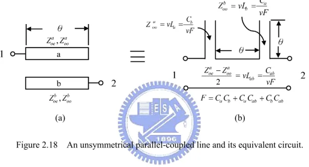
This section considers several types of coupled transmission lines with arbitrary lengths and their equivalent circuits. For designing bandpass filters with SIR in which lines are coupled in parallel or antiparallel, it’s necessary to find the relationship between even and odd mode impedance/admittance in the coupled lines and the impedance/admittance inverter parameters. With the equivalent circuits, we can design the bandpass filter more easily. In this section, the equivalent transmission-line circuit will be represented by two-wire lines. In each case, the characteristic impedance or admittance of the transmission line is shown, together with the electrical length θ . Meanwhile, the unsymmetrical-coupled line with different widths is also discussed [12].
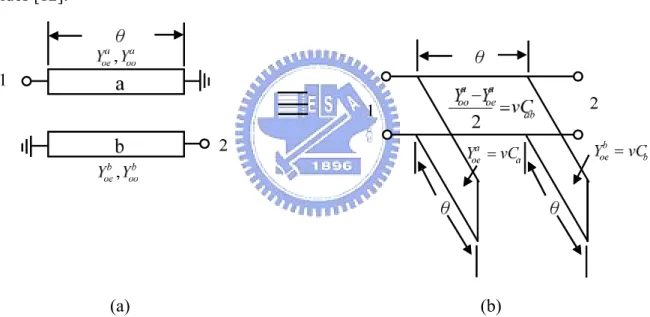
2.5.1 Equivalent Circuit of Parallel-Coupled Line
Figure 2.18(a) shows the parallel-coupled section generalized to cover the case where the two lines may be of different widths and its equivalent circuit is shown in Figure 2.18(b) [14], [15]. The parameter v refers to propagation velocity in media whileCa,Cb,and Cab are the line capacitances per unit length as defined inFigure 2.17. Note that Ca
is the capacitance per unit length between Line a and ground.Cb is the capacitance per
unit length between Line b and ground while Cab is the capacitance per unit length
between Line a and Line b. The definition of La, Lb are the self-inductances per unit
length of Line a and b, while Lab is the mutual inductance per unit length between the
parallel-coupled lines. Since the line capacitances are more convenient to deal with, the line impedances of the equivalent open-wire circuit are also given in terms of Ca, Cb,
and Cab. From Figure 2.18(b), it’s apparent thatwhen θ is 90 degrees, the series stubs
28
a
C Cb
ab
C
Figure 2.17 An unsymmetrical pair of parallel-coupled lines. C ,a C and b C are line ab
capacitances per unit length.
(a) (b)
Figure 2.18 An unsymmetrical parallel-coupled line and its equivalent circuit.
On the other hand, the symmetric parallel-coupled line relating to the lines with the same width is depicted in Figure 2.19(a). In this case, a b
oe oe oe
Y =Y =Y and
.
a b
oo oo oo
Y =Y =Y It’s clear to see that the even- and odd-mode admittance can be
simplified as Yoe , Yoo , and the equivalent circuit is expressed by two single
transmission lines of electrical length θ , admittance Y0 and admittance inverter
29 θ θ 90 − D
,
oe ooZ
Z
Y
oe,
Y
oo θ (a) (b)Figure 2.19 A symmetrical parallel-coupled line and its equivalent circuit.
The ABCD matrix for Figure 2.19(a) and (b) can be expressed as
[ ]
(
) (
)
(
)
2 2cos2 1 cos 2 sin , 2sin cos oo oe oo oe oo oe oo oe oo oe oo oe a oo oe oo oe oo oe oo oe Y Y Y Y Y Y j Y Y Y Y Y Y F Y Y j Y Y Y Y Y Y θ θ θ θ θ + − + + ⋅ − − = + ⋅ ⋅ − − (2.47)[ ]
2 0 0 0 0 0 2 2 0 0 0 0 0 1sin cos sin cos
.
sin cos sin cos
b Y Y J J j Y J Y Y J F Y J J Y jY J Y Y J θ θ θ θ θ θ θ θ + − = − + (2.48)
Then equalizing each corresponding matrix element, we can obtain [8]
2 2 0 2 2 0 0 0 1 cot , 1 csc oe J Y Y Y J J Y Y θ θ − = + + (2.49) 2 2 0 2 2 0 0 0 1 cot . 1 csc oo J Y Y Y J J Y Y θ θ − = − + (2.50)
In Figure 2.20, placing short-circuits on diagonal ports instead, the dual situation of the circuit in Figure 2.18 holds. Similarly, the even- and odd-mode admittances are
30
depicted and the electrical length is θ . The equivalent two-wire circuit is shown in Figure 2.20(b) accordingly with the parameters defined in Figure 2.18 [14],[15]. In this case, when θ is 90 degrees, each of the series stub acts like a resonator of parallel resonance.
Meanwhile, in the case of symmetrical coupled lines, the circuit schematic diagram is simplified as Figure 2.21(a) while the even- and odd-mode impedances are represented as
oe
Z , Zoo. This section can be approximately modeled by the equivalent circuit shown in
Figure 2.21(b) including an impedance inverter parameter K together with two single transmission lines of electrical length θ and impedance Z0, connected in series on both
sides [12].
(a) (b)
Figure 2.20 An unsymmetrical parallel-coupled line and its equivalent circuit. θ θ θ 90 − D
,
oe ooZ
Z
Y Y
oe,
oo (a) (b)31
Similar, equating the ABCD matrixes in Figure 2.21, design formulas correspond to
, oe oo Z Z can be derived as 2 2 0 2 0 0 0 1 cot , 1 csc oe K Z Z Z K K Z Z θ θ − = − + (2.51) 2 2 0 2 0 0 0 1 cot . 1 csc oo K Z Z Z K K Z Z θ θ − = + + (2.52)
2.5.2 Equivalent Circuit of Antiparallel-Coupled Line
Different from the parallel-coupled lines described in previous section 2.4.1, we introduce the antiparallel coupled-line circuits which are terminated with short circuits or open circuits on the same side. The circuit scheme shown in Figure 2.22(a) is the asymmetrical coupled line with an open-circuit termination on the same side while the equivalent two-wire circuit is shown in Figure 2.22(b). The even- and odd-mode impedance with electrical length θ are depicted. When θ is 90 degrees, the circuit operates like an all-stop structure.For a symmetrical case, Figure 2.23(a) illustrates even- and odd-mode admittance
oe
Y , Yoo of the antiparallel coupled-line section with electrical length θ . The equivalent
circuit is shown in Figure 2.23(b) which is expressed by an admittance inverter parameter J as well as two open stubs with electrical length θ and impedance Z0 which shunted
32 ab C vF b C vF a C vF (a) (b)
Figure 2.22 An unsymmetrical parallel-coupled line and its equivalent circuit.
,
oe ooZ
Z
Y Y
oe,
oo 90 − D θ (a) (b)Figure 2.23 A symmetrical parallel-coupled line and its equivalent circuit. Similar with the previous section, we can derive the formulas relate to Yoe and Yoo
as follows: 0 0 1 cot , oo Y J Y = +Y θ (2.53) 0 0 1 cot . oe Y J Y = −Y θ (2.54)
It’s noted that when θ is equal to 90 degrees that means Yoe=Yoo, no coupling
exists in the coupled line. Therefore, (2.53) and (2.54) are applicable except that θ is 90 degrees.
33
side are shorted which is the dual of the circuit in Figure 2.22. The equivalent circuit is expressed as Figure 2.24(b). In this case, when θ is 90 degrees, the circuit operates like an all-stop structure which is similar with that in Figure 2.22.
Futhermore, if the coupled line is symmetric , it’s obvious that a b
oe oe oe
Y =Y =Y and
a b
oo oo oo
Y =Y =Y as shown in Figure 2.25(a). The corresponding equivalent circuit shown
in Figure 2.25(b) consists of two shunt stubs with short-circuit terminations on both sides and an admittance inverter between them. [12]
a oe a Y =vC
(a) (b)
Figure 2.24 An unsymmetrical antiparallel-coupled line and its equivalent circuit.
,
oe ooZ
Z
Y Y
oe,
oo θ 90 − D (a) (b)34
Finally, we can acquire the formulas relating to Yoo and Yoe,
0 0 1 tan , oo Y J Y = +Y θ (2.55) 0 0 1 tan . oe Y J Y = −Y θ (2.56)
When θ is equal to 90 degrees, Yoo and Yoe tend to be infinite. Therefore, the
design formulas in Figure 2.25 is not suitable for the case θ = .
2.6 Second-Order Gap Coupling Bandpass
Filter
In this section, we introduce an example for the second-order bandpass filter using the theory discussed in previous sections. First, utilizing the theory about λ SIR / 2
described in Section 2.1.2, we can easily design the SIR by giving an impedance ratio R and the electrical length θb. For example, choose Zb =50ohm, Za =70ohm( R <1) and
60o b
θ = with center frequency 3GHz, 6% bandwidth and 0.1 dB ripple. From (2.3), we can obtain 22.41o a θ = . CLIN TL2 F=f GHz E=E0 Zo=Zoo01 Ohm
Ze=Zoe01 Ohm TermTerm2
Z=50 Ohm Num=2 Term Term1 Z=50 Ohm Num=1 TLIN TL4 F=f GHz E=EM Z=Zm Ohm CLIN TL3 F=f GHz E=E0 Zo=Zoo12 Ohm Ze=Zoe12 Ohm TLIN TL5 F=f GHz E=EM Z=Zm Ohm CLIN TL1 F=f GHz E=E0 Zo=Zoo01 Ohm Ze=Zoe01 Ohm
Figure 2.26 Circuit configuration of the second-order gap coupling filter.
35
correspond to open-circuited parallel coupled-line. Therefore, we can approximately utilize the equivalence shown in Figure 2.19. On the other hand, the second coupled section belongs to the open-circuited antiparallel coupled-line discussed in Section 2.5.2, so that the equivalence shown in Figure 2.23 can be used here. The consideration about
b
θ relating to the antiparallel and parallel coupled-line sections in the bandpass filter is that θb should be shorter then due to the accuracy about design equations. Now, we can construct the equivalent circuits with admittance inverters as depicted in Figure 2.27. The second-order coupled-line filter is equivalent to several admittance inverters separated by transmission-line sections which is actually the λ/ 2-type SIR shown in Figure 2.4(a).
Figure 2.27 The overall equivalent circuit of the second-order gap coupling filter.
Since the SIR structure exists the parallel type of resonance physically, we can then use the theory introduced in Section 2.2 that all the resonators can be represented by the susceptance slope parameter “b”. Thus, we are going to calculate the parameters b. Figure 2.27 shows that b01 and b34 are the slope parameters seen by J01 and J34
looking into the resonator whereas b12 and b23 are those seen by J12 looking into the resonator on both of its sides. Obviously, b01 =b34 and b12 =b23. Therefore we only need
36 for b a Z R Z
= , the input admittance seen by inverter J01 looking into the resonator is,
01 2 2 2 01
2( tan tan )( tan tan ) (1 tan )(1 tan ) 2(1 ) tan tan
a b b a b b a b a R R Y jY jB R R θ θ θ θ θ θ θ θ + − = = − − − + (2.57) 0 0 01 01 2 dB b d ω ω ω ω = = 2 2 2 2 2 2
tan 2 ( csc sec ) 2 sec 2 ( cot tan ) .
2 tan 2 (1 ) (tan cot )
b b a b b a a b b a b b Y R R R R θ θ θ θ θ θ θ θ θ θ θ × + + × − + = × + + − (2.58)
where B01 is the susceptance component of the input admittance. In the case of UIR
(uniform impedance resonator), (2.58) can be simplified as follows:
01 . 2 b Y b =π (2.59) Next, assume the input admittance seen from J12 towards left is Y12 derived as
2 2
12 12
tan 2 tan cot 2 cot 2 tan b b a b a b R R Y jY jB R θ θ θ θ θ − + = = − (2.60) Then, 0 0 12 12 2 dB b d ω ω ω ω = = 2 2
sec (2 cot 2 2 tan ) 4 tan csc 2
2 cot 2 tan b b b a b a b a a b Y R R R θ θ θ θ θ θ θ θ θ − − = − (2.61) Also, in the case of UIR, (2.61) can be simplified as follows:
2 01 sec . 2 b b Y b =π θ (2.62) Therefore, given the impedance ratio and electrical length of SIR, the slope parameters from b01 to b34 shown in Figure 2.27 can be obtained definitely.
From (2.31) and (2.32), choose RS and RL to be port impedance 50ohm, with the
37
By symmetry, J12=J23. While J01, J12 and J23 are available and 0 1 1
50
Y = Ω− , with (2.49) , (2.50) , (2.53) and (2.54), the even- and odd-mode impedances for each of the coupled-line section can then be derived.
On the other hand, similar procedure can be used to design the bandpass filter using the coupled-line section with short-circuit terminations shown in Figure 2.21 and Figure 2.25. That is, the first and third coupled-line sections are replaced with the parallel coupled line depicted in Figure 2.21(a). Meanwhile, the second coupled-line section is substituted for the antiparallel coupled-line circuit in Figure 2.25(a). Furthermore, the
/ 2
λ SIR is considered as the short-end type SIR in Figure 2.5 which is different from the SIR used in Type I filter. Figure 2.28 illustrates the overall circuit scheme.
Term Term2 Z=50 Ohm Num=2 CLIN TL2 F=f GHz E=E0 Zo=Zoo01 Ohm Ze=Zoe01 Ohm TLIN TL5 F=f GHz E=EM Z=Zm Ohm CLIN TL3 F=f GHz E=E0 Zo=Zoo12 Ohm Ze=Zoe12 Ohm CLIN TL1 F=f GHz E=E0 Zo=Zoo01 Ohm Ze=Zoe01 Ohm Term Term1 Z=50 Ohm Num=1 TLIN TL4 F=f GHz E=EM Z=Zm Ohm
Figure 2.28 Circuit configuration of the second-order gap coupling filter.
Finally, cascading the equivalent circuits of parallel and antiparallel coupled lines, the complete equivalent circuits of the filter can be constructed as Figure 2.29.
Figure 2.29 The overall equivalent circuit of the second-order gap coupling filter. Different from Type I filter, the structure consists of two impedance inverters K01