國
立
交
通
大
學
物理研究所
博
士
論
文
利用掃瞄穿隧顯微鏡觀測雙原子分子在表面上的反應
Scanning Tunneling Microscopy Studies of Surface
Reactions of Diatomic Molecules
研 究 生:馮世鑫
指導教授:江進福 教授
林登松 教授
利用掃瞄穿隧顯微鏡觀測雙原子分子在表面上的反應
Scanning Tunneling Microscopy Studies of Surface
Reactions of Diatomic Molecules
研 究 生:馮世鑫 Student:Shyh-Shin Ferng
指導教授:江進福 Advisor:Tsin-Fu Jiang
林登松 Deng-Sung Lin
國 立 交 通 大 學
物 理 研 究 所
博 士 論 文
A ThesisSubmitted to Institute of Physics College of Science National Chiao Tung University in partial Fulfillment of the Requirements
for the Degree of Doctor
in Physics October 2008
Hsinchu, Taiwan, Republic of China
利用掃瞄穿隧顯微鏡觀測雙原子分子在表面上的反應
學生:馮世鑫 指導教授:江進福
林登松
國立交通大學物理研究所博士班
摘要 本論文主要是利用掃瞄穿隧顯微鏡(STM)觀察分子在表面上的作用與反應, 其中的課題包括分子結合脫附、表面結構相變化、分子吸附、熱原子動力學以及 基底大小對量子點成長的影響。本論文各章節大概編排如下:第一章簡介分子在 表面上的吸附以及脫附動力學。第二章描述實驗上的儀器架構、STM 操作原理、 樣品製備方式以及探針脫附的技巧。而第三章到第五章是展現實驗結果以及討 論。第六章為實驗結果的結論以及進一步的討論。 在探討表面結構相變化的部分,氫原子在 Si(100)表面上可使表層矽原子鍵 結一個氫原子(monohydride)或者鍵結兩個氫原子(dihydride),而這兩種結 構的組合可讓 Si(100)表面上形成三種穩定的相位:(1×1)、(3×1)以及(2×1)相 位,氫原子的覆蓋率分別為 2、1.33 以及 1 個表層矽原子密度。本實驗探討(1× 1)和(3×1)相位是如何相變到(2×1)相位,以及氫原子由表面熱脫附的動力學機 制,做法是加熱擁有(1×1)和(3×1)相位的樣品,使表面上的結構相變至(2×1)相 位,再利用掃瞄穿隧顯微鏡觀察表面上的變化。結果顯示氫分子由 dihydride 區域脫附時(由 1×1 區域脫附),兩個氫原子來自於相鄰兩個 dihydride 內側的附是在樣品溫度較高時,兩個氫原子來自於同一個 dimer 上的氫原子。 在研究分子吸附動力學部分,首先討論碘分子在乾淨 Si(100)表面上的吸附 動力學。碘分子覆蓋率較低時,結果顯示兩個碘原子吸附在相鄰同排 dimer row 同側上的活性鍵的機率最高。當碘的吸附量增加後,最高的覆蓋率只能達到 0.92 個表層矽原子密度。為了進一步探討碘分子以及氯分子的吸附動力學,我們在覆 蓋了氫原子的 Si(100)表面上製備出擁有孤立活性鍵的表面,這些活性鍵可以是 單一的、成對的、成串的或是長鍊狀的。當碘分子和氯分子與這些活性鍵作用後, 我們觀察到兩種分子是以不同的動力學做吸附。對於碘分子的吸附,兩的碘原子 的吸附必須同時產生,分子鍵才會斷裂。所以表面上必須存在兩個且鄰近的活性 鍵,碘分子才會裂解吸附。對於氯分子而言,兩個氯原子的吸附是可以單獨進行, 所以表面上只需要存在單一個活性鍵,即可使吸附反應發生。反應過程往往是一 個氯原子先與活性鍵鍵結,而另一個氯原子可以離開表面,也可以與周遭的原子 產生新的反應。 本論文利用真實空間以及原子解析度的影像來探討表面化學反應,其中的利 用孤立活性鍵來探討分子吸附動力學更是第一次提出,這樣的表面結構提供一個 很好的介面來研究氣體與固體反應動力學。
Scanning Tunneling Microscopy Studies of Surface
Reactions of Diatomic Molecules
Student:Shyh-Shin Ferng Advisor:Tsin-Fu Jiang
Deng-Sung Lin
Institute of Physics National Chiao Tung University
Abstract
The objective of this thesis focuses on the fundamental issues in surface reactions by using scanning tunneling microscopy (STM). The scientific issues include recombinative desorption, structure phase transition, dissociative adsorption, abstractive adsorption, hot atom motion, and size-dependent quantum-dot growth. The thesis is organized as following: Chapter 1 introduces the common mechanisms of molecules adsorption and desorption on the surface. Chapter 2 describes the experimental setup employed during this research. The STM operating principles, sample preparation procedures, and STM lithography techniques are also explained. The detailed results and discussions of each issue are presented in Chapter 3, 4, and 5. Finally, Chapter 6 summarizes the results and further discussions.
For the discussion of structure phase transition on the Si(100) surface, monohydrides dimers (SiH) and dihydride (SiH2) species can form an ordered mixture
and monohydride species are investigated. Desorption from dihydrides proceeds by recombination of two H atoms coming separately from two adjacent dihydrides. This process is geometrically forbidden for the (3 × 1) surface, but becomes possible with a switch of a dihydride with a neighboring monohydride dimer. Desorption from monohydrides occurs at a higher temperature, and proceeds by recombination of the two H atoms on a given monohydride dimer.
In the discussions of molecule adsorption mechanisms, I2 on a prototypical
semiconductor surface is observed. Adsorption of I2 on the same side of neighboring
dimer is favored than on one dimer with the ratio1 at low coverage. After further I2
exposure, the maximum iodine coverage is 0.92 ML. To distinguish the adsorption geometry for I2, single dangling bond pairs that are fabricated on H/Si(100) surface are
used for I2 adsorption. Different adsorption mechanisms of I2 and Cl2 are demonstrated
with I2 and Cl2 reaction to dangling bonds in isolation or organized in pairs, clusters, or
arrays. Iodine chemisorption is predominantly a pair process involving the bonding of the two I atoms in a I2 molecule onto two neighboring dangling bonds. In sharp
contrast, adsorption of Cl2 is dominated by the bonding of just one Cl atom in a Cl2
molecule, with the other Cl atom either leaving the surface or migrating to a nearby area to cause further reactions.
This thesis gives the real-space images and detailed atomic processes by in situ studies. The adsorption mechanisms of molecules on various initial active site configurations are first reported. This approach points to opportunities for systematic investigations of the atomistics of gas-surface reactions.
Acknowledgements
感謝指導老師林登松教授在我碩、博期間的指導與教誨,六年的相處讓我獲 益良多。感謝實驗室夥伴鎧銘學長、明峰、昌廷、仁陽在這些年來的幫助與指教, 以及謝謝宏道、靖勛、中廷以及展源的陪伴,讓我博士生涯的最後一年充滿歡樂, 也要感謝曉穎、欣樺、靈櫻以及歷屆畢業學弟妹的照顧。 感謝我的父親馮國添先生、母親吳美彩女士以及家人在這些年來的支持,讓 我無後顧之憂地專注於實驗研究上,最終完成博士學位。謝謝女友君黛一路上的 陪伴與等待,以及君黛父母張航雲先生與溫幼霞女士的關心及照顧。也感謝所有 踢球的朋友,讓我可以不時地活動筋骨以及抒解每星期的疲勞。I would also like to thank Karina, Jörg, Michael, Heiko, Fatih, Xin, Christopher and Carsten for your help and guidance during I stayed in Germany.
Contents
摘要...i
Abstract... iii
Acknowledgements ...v
List of Figures... viii
Chapter 1 Introduction...1
1.1 Motivation...1
1.2 Si(100) surface ...8
1.3 Literature Review...10
Chapter 2 Experimental Apparatus ...16
2.1 Vacuum System...16
2.2 Scanning Tunneling Microscopy (STM) ...18
2.3 Preparing STM tips ...21
2.4 Sample preparation ...23
2.5 Nanostructuring...27
Chapter 3 Atomistic View of the Recombinative Desorption of H2 from H/Si(100) ...30
3.1 Introduction...30
3.2 Experiment...33
3.3 Results and Discussion ...34
3.3.1 Recominative desorption of H2 form H/Si(100) ...34
3.3.2 Evolution of two-dimension structure phase transition (1 × 1) → (2 × 1) and (3 × 1) → (2 × 1)...40
3.4 Conclusion ...46
Chapter 4 Unsaturated Characteristic of the I/Si(100) Surface via Dissociative Adsorption Mechanism ...47
4.1 Introduction...47
4.2 Experiment...49
4.3 Results and Discussion ...50
4.3.1 I2 dissociative adsorption on Si(100) surface...50
4.3.2 Presence of isolated single danglings ...57
4.3.3 Maximum distance of two reactive sites allowed for I2 dissociative adsorption...60
4.4 Conclusion ...64
Chapter 5 Topographically Constrained Adsorption and Reaction Mechanisms of I2 and Cl2 on the Si(100) Surface...65
5.1 Introduction...65
5.2 Experiment...66
5.3 Results and Discussion ...67
5.4 Conclusion ...77
Chapter 6 Conclusion ...78
Appendix A Growth Behaviour of Ge Nano-islands on The Nanosized Si{111} Facets Bordering on Two {100} Planes ...81
A.1 Introduction...81
A.2 Experiment ...83
A.3 Results and Discussion...85
A.3 Results and Discussion...85
A.3.1 The formation of well-confined {111} surface ...85
A.3.2 Ge nano-islands on the (100) planes ...87
A.3.2 Ge nano-islands on the {111} planes ...89
A3.4 Conclusion ...96
List of Figures
Fig. 1.1 Schematic diagram showing normal surface reaction. ...2
Fig. 1.2 Potential energy curve for the diatomic molecule adsorption on the surface...3
Fig. 1.3 Potential energy curves of non-activated and activated adsorption...4
Fig. 1.4 Three normal adsorption mechanisms...5
Fig. 1.5 If the surface can be saturated via dissociative adsorption mechanism. ...6
Fig. 1.6 H atoms recombinative desorption from the surface and monohydride species rearrangement during phase transition...7
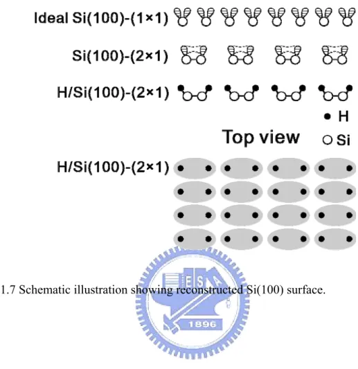
Fig. 1.7 Schematic illustration showing the reconstructed Si(100) surface...9
Fig. 1.8 Proposed mechanism for the conversion of H/Si(001)-3×1 to H/Si(001)-2×1 ...10
Fig. 1.9 Possible initial configurations following loss of two H atoms...11
Fig. 1.10 TPD spectra of H2 desorption obtained from H-saturated Si(100)...12
Fig. 1.11 Dissociative adsorption of a Cl2 molecule on the buckled dimer. ...13
Fig. 1.12 The structures observed in STM experiments after dissociative adsorption of Cl2 on Si(100). ...14
Fig. 1.13 Initial stages of Cl2 adsorption showing the different Cl adsorption sites....15
Fig. 1.14 TOF showing abstractive adsorption)...15
Fig. 2.1 Schematic illustration the top view of the UHV chamber. ...17
Fig. 2.2 Schematic illustration of the STM system...20
Fig. 2.3 The sketch of the etching procedure for the tungsten (W) tip.. ...22
Fig. 2.4 STM image of H/Si(100)-(2 × 1) surface with several dangling bonds. ...25
Fig. 2.5 STM image of H/Si(100)-(3 × 1) surface. ...26
Fig. 2.8 Array of DBs was fabricated on a H terminated Si(100)...29
Fig. 3.1 Schematic diagrams showing (1 × 1) dihydride, (2 × 1) monohydride, and (3 × 1) mixed monohydride-dihydride phases, and χ, δ, and μ reactions……….…32
Fig. 3.2 STM images after a (3 × 1) sample has been annealed at 570 K for different times...35
Fig. 3.3 Closeup images showing desorption processes from dihydride domain and monohydride domain ...37
Fig. 3.4 Time evolution of H/Si(100) surface after sample was heated at 570K for different time...41
Fig. 3.5 Coverage for vacancies, (1 × 1), (3 × 1)), and (2 × 1) domains as functions of annealing time at 570 K ...44
Fig. 3.6 STM image near step edge after nominal H/Si(100)-(3 × 1) is annealed...45
Fig. 4.1 STM images showing I2 adsorption on the Si(100) surface at different coverage ...52
Fig. 4.2 Zoom-in images showing some configurations at low and high coverage surface ...55
Fig. 4.3 Coverage of iodine and isolated SDB as function of I2 exposure ...56
Fig. 4.4 Showing the population of each new adsorption site.. ...59
Fig. 4.5 Showing before and after 1.32 L I2 expose on single DBs ...62
Fig. 4.6 Showing before and after 1.32 L I2 expose on series of SDB pairs...63
Fig. 5.1 Showing before and after I2 expose on single and paired DBs. ...68
Fig. 5.2 Showing before and after I2 expose on cluster of dangling bonds.. ...69
Fig. 5.6 Showing before and after Cl2 expose on a stripe of dangling bonds ...76
Fig. A.1 Process flow chart for the fabrication of 2D arrays of rectangular mesas and negative pyramids. ...84
Fig. A.2 AFM z-height profiles over the mesa side walls following etching in KOH + IPA solution...86
Fig. A.3 Derivative AFM images displaying Si mesas after Ge growth. ...88
Fig. A.4 Zoom-in three-dimensional images over the {111} facet...91
Fig. A.5 Zoom-in derivative images over the {111} facet...92
Fig. A.6 Three-dimensional AFM images showing a negative pyramid following Ge growth. . ...95
Chapter 1 Introduction
Why and how do molecules break the molecular bond and adsorb on the surface? This is a simple question and indeed very important for chemical industry and device processing. To answer this question, extensive theoretical and experimental studies have been carried over the half-century. However, most experimental works focused on the examinations of diffraction spectra or the detection of the atoms/molecules scattered from the surface after reactions; these indirect measurements can’t reflect the real dynamics of the adsorbates. For the theoretical studies, surface reactions are often too complex to be simulated since the molecule has various transitional states, vibration states, or rotation states, and surface phonons also must be taken in consideration. After STM was invented, it has widely been used to understand the fundamental surface reaction by providing real-space images. However much detailed reaction dynamics are still not clear.
In thesis, I will elucidate the surface reaction of H2, Cl2, and I2 on Si(100) surface by
patterning various dangling bond geometry. These studies include recombinative desorption, surface phase transition, dissociative adsorption, abstractive adsorption, hot atom motion, and cascading reaction.
1.1 Motivation
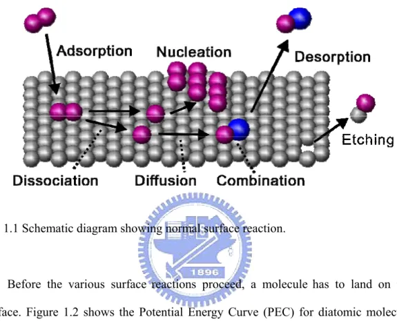
A surface reaction is complicated; it involves the interaction between the molecule and the substrate, the molecule and adsorbates, and adsorbates and adsorbates. Figure 1.1 shows a few common surface reactions. An incident molecule first adsorbs on the surface if the total energy decreases after formation of surface
adsorbate and desorbs away from the surface. Sometimes, the adsorbed atom could extract the substrate atom and create a vacancy site.
Fig. 1.1 Schematic diagram showing normal surface reaction.
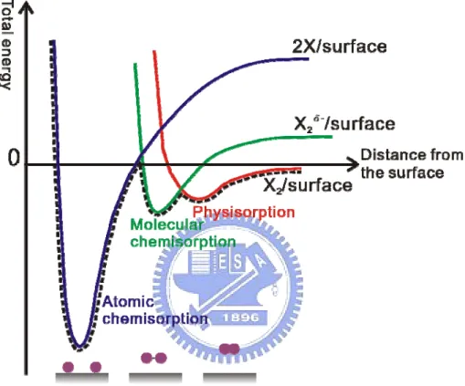
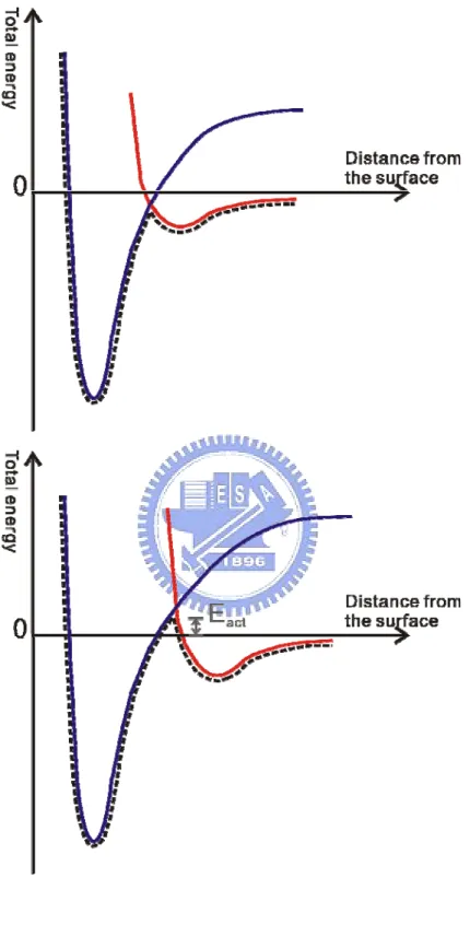
Before the various surface reactions proceed, a molecule has to land on the surface. Figure 1.2 shows the Potential Energy Curve (PEC) for diatomic molecule adsorption on the surface. There are three different PECs, molecular physisorption PEC, molecular chemisorption PEC, and atomic chemisorption PEC. Typically an incoming molecule is trapped in a physisorption well when molecule comes from the gas source to the vicinity of a surface. If there is a charge transfer to the molecule, the molecule can then enter the molecular chemisorption well. The molecular bond will break as the total energy is further decreased after new chemical bonds are formed with the surface. Whether a molecule is adsorbed or not also depends on the activation barrier. Figure 1.3 shows that there are two kinds of adsorption, non-activated and activated adsorption. For non-activated cases, the direct chemisorption occurs. In the later case, an activation barrier prevents the molecule bond to break even though the molecule can
be trapped in a precursor well as precursor-mediated state. The precursor state may migrate on the surface and then either leave the surface or is adsorbed on somewhere else with a smaller barrier.
Fig. 1.2 Schematic illustration showing potential energy curve for the diatomic molecule adsorption on the surface.
Fig. 1.3 Schematic illustration showing potential energy curves of non-activated and activated adsorption. Eact is the activation barrier for adsorption.
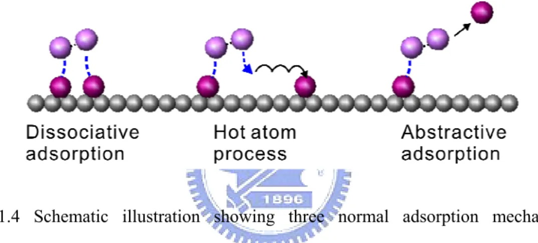
The adsorption mechanisms are commonly classified into there categories: dissociative adsorption, abstractive adsorption or hot atom process, as shown in Fig. 1.4. The dissociative adsorption means the molecular bond broken as two atom-substrate bonds are created. The hot atom process means the adsorbed atoms land at a distance in between. In the other words, two atoms migrate a short distance before they settle down. In an abstractive adsorption, one atom of the molecule is adsorbed on the surface, while the other atom leaves the surface.
Fig. 1.4 Schematic illustration showing three normal adsorption mechanisms: dissociative adsorption, hot atom process, and abstractive adsorption.
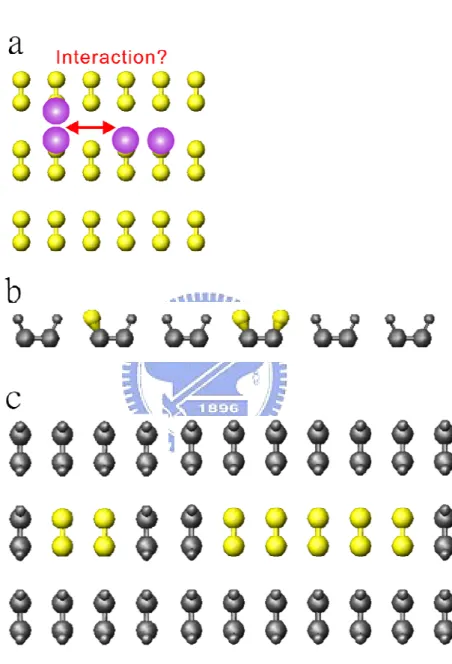
As discussed above, the surface reaction or adsorption mechanisms are complicated, and some adsorbates are mobile. The final state that we obtained could be the result after adsorbate-adsorbate interaction, as shown in Fig. 1.5(a). In order to simplify the reaction and separated study each reaction, we fabricated several isolated reactive sites, i.e. isolated dangle bond, as shown in Fig. 1.5(b).
There are many interesting questions about diatomic molecule adsorption on this special configuration. For examples, if diatomic molecule adsorb on single DB sites? If
Fig. 1.5 Schematic illustration showing if the surface can be saturated via dissociative adsorption mechanism.
In addition, I also studied the recombinative desorption of diatomic molecule. Here we chose the hydrogen molecule as our main actor. There are three different H/Si(100) phase with different mixture of monohydride and dihydride. What we are interested in is how two H atom organize themselves to recombinatively desorb away from the surface, as illustrated in Fig. 1.6.
In thesis, the research is based on H/Si(100) surface, so I will discuss this surface first and including of hydrogen recombinative desorption. Then I will demonstrate that I2 adsorption on clean Si(100) surface. Finally, I compare the different adsorption
mechanisms of I2 and Cl2 using isolated or paired dangling bonds on H-terminated
surface. The appendix includes a study of growth behaviour of Ge nano-islands on the nanosized Si{111} facets bordering on two {100} planes. The reason to organize this research in the appendix is that the reaction gas GeH4 is a more complex gas, not a
1.2 Si(100) surface
If one cleaves the silicon crystal along the (100) direction, two valence bonds of each exposure surface Si atom will be broken and become so-called dangling bonds on the surface. Therefore, every silicon atom in the unreconstructed surface has two dangling bonds and two valence bonds, as shown in Fig. 1.7. The unreconstructed surface has a 1×1 structure. In this 1×1 structure, the density of the dangling bonds is high (two dangling bonds per atoms), therefore the surface energy is high and the 1×1 structure is unstable. To reduce the numbers of the dangling bonds, the first layer atoms in the surface will reconstruct. By this way, the surface energy will be lower and the 1×1 structure will be more stable.
Upon reconstruction, two adjacent atoms form a strong sigma bond by combined one of the two dangling bonds. The numbers of dangling bonds is reduced by 50%. These remaining dangling bonds can further form a weak π bond. The 1×1 structure of the surface have transformed into 2×1 structure. These bonded pairs of Si atoms are called dimers. These dangling bonds are chemically reactive. An example is shown in 1.7: every dangling bond trap a hydrogen atom after hydrogen expose.
1.3 Literature Review
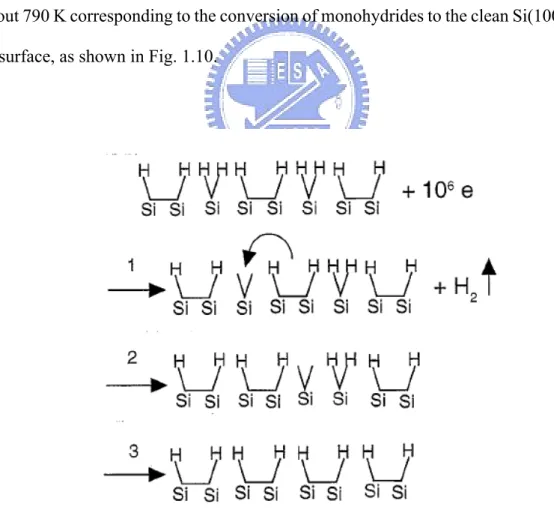
How are two H atoms from a dyhydride recombinatively desorbed from the Si(100) surface? Scientists used several methods to answer this question [1,2,3,4]. Chen et al. proposed that the H2 desorbs first as dihydride species, then the neighboring
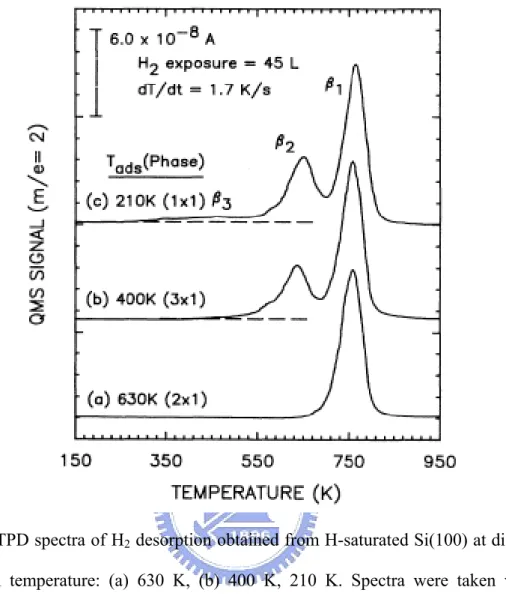
σ-bond switchs, and finally a monohydride species is formed, as shown in Fig. 1.8. They also calculated the total energy of each configuration during conversion, as Fig. 1.9 depicts. Their results shows that the low energy reaction intermediate is either bare Si atom or bare dimer. Cheng et al. provided a temperature-programmed desorpton (TPD) studied which have shown two desorption peaks: a β2 peak at about 680 K
corresponding to the conversion of dihydrides to monohydrides, and a β1 peak at
about 790 K corresponding to the conversion of monohydrides to the clean Si(100)-(2 × 1) surface, as shown in Fig. 1.10.
Fig. 1.8 Proposed mechanism for the conversion of H/Si(001)-3 × 1 to H/Si(001)-2 × 1. Copied by T. C. Shen, Surf. Sci. 390, 35 (1997).
Fig. 1.9 Possible initial configurations following loss of two H atoms from a DMD unit. The energies (relative to the 2×1 surface) are from the DFT calculations described in the text. Copied from T. C. Shen, Surf. Sci. 446, 211 (2000).
Fig. 1.10 TPD spectra of H2 desorption obtained from H-saturated Si(100) at different
adsorption temperature: (a) 630 K, (b) 400 K, 210 K. Spectra were taken with a heating rate of 1.7 K/s after the crystal was cooled down to 130K. Copied from C. C. Cheng, Phys. Rev. B 43, 4041 (1991).
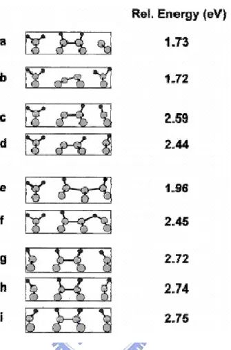
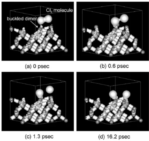
The interaction of halogen molecules with Si surface is scientifically and technologically important. This system has been studied by various surface analysis techniques over the years [5,6,7]. Mori et al. use first-principle molecular-dynamics to simulate the adsorption with picosecond resolution, as shown in Fig. 1.11. They demonstrated that Cl2 and F2 molecules adsorb dissociatively at dangling bonds of a
buckled dimer with no energy barrier, so that the buckled dimer becomes geometrically flat. Chan etc. calculated the total energy of different adsorption
configurations, as shown in Fig. 1.12. The energy ordering is Type I ﹤Type IIa ﹤ Type IIIa ﹤Type IIIb ﹤Type IIb. Type I is the most stable because it only breaks one weak π bond between the dimer silicon atoms, while the other configurations break two. STM study was performed by Yates etc., as in Fig. 1.13. The adsorption of two Cl atoms on Si dimer sites in adjacent silicon dimer rows was found to be kinetically favored. In 1995, Li et al. identified a new adsorption mechanism: atom abstraction, Fig. 1.14. In this process, one atom of the molecule is adsorbed on the surface, while the other atom leaves the surface.
Fig. 1.11 Dissociative adsorption of a Cl2 molecule on the buckled dimer of the Si(0 0
Fig. 1.12 The structures observed in STM experiments after dissociative adsorption of Cl2on Si(100). The broken line encircles a Si–Si dimer, while the dark circles indicate
the adsorption sites of Cl atoms, which could be on the same dimer as in Type I, or across the same dimer row as in Type IIa and IIb, or across two dimer rows as in Type IIIa and IIIb. Each type of structure is putin a 4×4 surface lattice, which is the lattice used in our calculation. The number in parentheses is the calculated total energy for each structure. Copied from S.P. Chan etc., Chem. Phys. Lett. 318, 15 (2000).
Fig. 1.13 Image of 46×55 Å2 region of the Si(100) surface at initial stages of Cl2
adsorption showing the different Cl adsorption sites. (a) Filled-state STM image at a sample bias of -1.5 V and a tunneling current of 0.05 nA. (b) Schematic identification of the observed features. Copied from J. T. Yates, Jr. etc., Phys. Rev. B 58, 7950 (1998).
Fig. 1.14 (a) Signal at m/e = 19 and 38 (scaled by 0.25) recorded at θi= 0° andθd=
Chapter 2 Experimental Apparatus
2.1 Vacuum System
The experiments were carried out in the ultra-high vacuum (UHV) system with a base pressure of 1.0 × 10⁻¹⁰ torr. The whole system consists of commercial STM, pumping system, and gas source. The STM system with an indirect heating stage and thermal couple can give option for measurement with the temperature range from room temperature to 650 K. The pumping system includes dry pump, an oil pump, a turbo pump, a titanium sublimation pump (TSP), and an ion pump. The gas sources contain H2, I2, Cl2, and HCl.
The chamber is divided into three parts: Loading chamber, Main chamber, and Gas line as shown in Fig. 2.1. Loading chamber is used to transfer tips and samples. Main chamber is for preparing sample and STM measuring. Gas line is for quick exchanging gas source without venting main chamber. Gas source was introduced into the chamber through a precision leak valve.
In order to obtain ultra-high vacuum, the dry pump and turbo pump were first used to evacuate the chamber from the atmosphere to high vacuum around 10-6 torr. A baking procedure was followed to the temperature ~120℃ for 24 hours. After the pressure started to drop off, most moisture was pumped out, closing the valve between the Loading chamber and Main chamber. Then ion pump with the help of TPS during cool down was supported to achieve ultra-high vacuum.
For the tips and samples transferring, the tips and samples were placed into the Loading chamber, and then we bake Loading chamber to ~130℃ for 12 hrs to out gas the moisture from the tip holder. After the Loading chamber cool down to room temperature, we transport the tips and samples into Main chamber. Various treatments will be treated depending upon the type of sample used in the experiment.
2.2 Scanning Tunneling Microscopy (STM)
Scanning Tunneling Microscope (STM) was invented by G. Binnig and H. Rohrer in 1981, they shared the 1986 Nobel Price in Physics for their invention. With the abilities of real-space surface image and atomic resolution, STM has been widely used in many fields, such as condensed-matter physics, chemical and biology.
Base on quantum mechanical tunneling, a particle can penetrate a potential barrier with nonzero probability. Thus, a sharp conducting tip is brought so close to the probed surface with a gap of a few angstroms, and a bias voltage is applied between tip and sample. This allowing the wave function of tip electron state can overlap with those of the sample. The tunneling current is proportion to density state of the sample and tip, gap voltage, and distance between tip and sample, as followed [8]:
0 0 0 ( , ) F ( ) ( , ) ( , , ) F E eV T s E I r V ∝
∫
+ dEρ E+eV ρ r E T r E eV 2 0 ( , , ) s T r E eV =e−κ 2 2 1/ 2 [(2m / ) k ] κ = ϕ h + 1 1 [ ( ) ( )] 2 t s E 2 eV ϕ = ϕ ϕ+ − +ρs(ro, E): density of states of the sample
ρT(E, ev): density of states of the tip
T(r0, E, eV): transmission probability of the electron
eV: applied bias voltage between tip and sample s(ro): tip-sample gap width
In the operating of STM, piezoelectric elements are used to control the tip to move in three orthogonal directions as schemed in Fig. 2.2. For the z direction, a feedback
circuit is used to modify tip height in order to maintain a constant current during the operating in constant current mode. The tunneling current with stable feedback current is sensitive to control the distance between tip and sample, and the tunneling current is followed exponential decay. Typically, a change of the gap by 1 Å results in the tunneling current by an order of magnitude. Which gives STM its remarkably high precision in positioning the tip (sub-angstrom vertically and atomic resolution laterally).
As the formula showing above, STM tunneling current is an integration of electronic density of states, i.e., the number of filled or unfilled electron states near the Fermi level, within an energy range determined by the bias voltage. Therefore, STM is a mapping of surface local density of electronic state and can identify and distinguish the atoms or molecules on the surface.
2.3 Preparing STM tips
Tungsten wire was chosen to fabricate a sharp tunneling tip for its high conductivity and hardness. A standard method for fabricating a STM tip is electro-chemical etching. For our experiment, W wire with a diameter of 0.5 mm and ~10% NaOH solution were used. Before etching a tip, the W wire was first etched in NaOH solution to clean surface oxide for a few seconds, One end of the W wire was inserted 1.5~2 mm below the solution level. A positive voltage, 7 V, is applied to the W wire as the anode and the cylindrical stainless steel is as the cathode as shown in Fig. 2.3. At the anode and cathode the following reactions take place:
Cathode: 6 H2O + 6e- → 3 H2(g) + 6 OH
-Anode : W(s) +8 OH- → WO42- + 4 H2O + 6 e-
The overall reaction is : W(s) + 2 OH- + 2 H2O → WO42-+ 3 H2(g)
The tungsten which is etched near the interface gets thinner and thinner, and then it is formed a neck shape. Therefore, the end of the wires falls off immediately below the solution surface. Eventually, we can obtain a sharp tip. The tip was soaked into DI water for 20 min and then washed with DI water and methanol.
Fig. 2.3 The sketch of the etching procedure for the tungsten (W) tip. The atomic scale tip can be made by the electro-chemical etching.
2.4 Sample preparation
The Si(100) samples was a Boron-doped wafer and had an resistivity of about 10 ohm-cm and doping concentration of 5 × 1015 cm-3. The miscut angle of the samples is 0.1°. The samples were mounted on holders which were made of Ta and Mo. Pure N2
gas gun was used to remove dusts on the samples’ surfaces. After loading into the vacuum chamber, the sample holder was degassed by indirect heating for 12 hours. Then, sample was direct heating up to ~600℃ using a small AC current (0.3 A) for 24 hours. In this procedure, the pressure never exceeded over 1.0 × 10⁻⁹ torr during sample degassing. To obtain typical Si(100)-(2 × 1) reconstructed surface, the samples was direct Joule heating at ~1400 K with subsequent radiation quenching, as Fig. 2.4.
For preparing H/Si(100) surface, atomic hydrogen was produced by backfilling the chamber to a background pressure of 2 × 10⁻⁷ Torr in the presence of a 1800 K tungsten filament, installed ~5 cm away from the sample. The flux of atomic hydrogen was not measured, and the exposure was recorded in terms of the background dosage of H2 inside the chamber. A H/Si(100)-(2 × 1) surface was generated by dosing 90 L
hydrogen on a clean Si(100)-(2 × 1) surface at 600 K, as shown in Fig. 2.4. While a mixed dihydride and monohydride structure is generated by further dosing 120 L hydrogen at ~400 K on H/Si(100)-(2 × 1) surface, as shown in Fig. 2.5. The sample temperature was measured via an infrared pyrometer.
2.5 Nanostructuring
The nanostructuring which were performed by STM on H/Si(100) surface through inelastic electron scattering mechanisms has been studied for several years [9, 10]. This technique can create localized reactive sites for exposing interesting molecules and the surrounding H-terminated area remaining unreacted. The desorption mechanism involves multi-quantum vibrational excitations of the H-Si bond under conditions of relatively high current and low energy tunneling electrons. In this thesis, the nanofabrications were created by an Omicron Nonostructuring program. The typical bias and current used for hydrogen desorption were 4.0 eV and 4.0 nA. The moving speed of the tip was 30-200 nm/ s. To fabricate a well-confined dangling bond lines, STM tip must be cleaned by making several times tip-forming until an empty state image with atomic resolution could be acquired. To overcome thermal drift, the tip must move along the scanning direction during nanostructuring, horizontal in our case as schemed in Fig. 2.6. Fig. 2.7 shows two dangling lines perpendicular to the dimer row direction, and Fig. 2.8 shows array of dangling bonds spread along the dimer row direction.
Fig. 2.7 Two DBs chains was fabricated on a H terminated Si(100) with a current–voltage pulse of +4.0 V/3.3 nA.
Chapter 3 Atomistic View of the Recombinative
Desorption of H
2from H/Si(100)
3.1 Introduction
Recombinative molecular desorption from a surface generally requires the assembly and organization of constituent atoms or molecular fragments on the surface into favorable precursor or predesorption configurations that are compatible with the free molecular shape [11,12]. Geometric constraints can play an important role in the pathway leading to a predesorption configuration, and this subject matter is of fundamental interest to surface physics and chemistry. In this Chapter, we discuss a study with scanning tunneling microscopy (STM) of the relevant atomistic issues associated with the desorption of H2 from hydrogenated
Si(100) surfaces. Being a simple model system, H/Si(100) has attracted intense interest, both experimentally and theoretically [13,14,15,16,17,18]. A detailed understanding of this system is also important from the technological point of view, as hydrogen termination and desorption are often employed in Si device processing. The key question is how two H atoms on H/Si(100) can organize themselves into a state conducive to recombination and desorption. The underlying principles are straightforward, as we shall demonstrate: the two H atoms must move sufficiently close to each other, and subsequent desorption must not leave behind a highly unstable surface configuration.
The relevant geometries are indicated schematically in Fig. 3.1(a)-Fig. 3.1(c). The clean Si(100) surface forms a (2 × 1) reconstruction consisting of parallel rows of dimers. Each surface Si atom has one dangling bond, and saturation of these dangling bonds with H leads to a (2 × 1) monohydride surface (or M M, where M stands for H Si). Further H adsorption - -
H-saturated surface is a (1 × 1) dihydride (D) surface [19,4 ,20]. There also exists an intermediate (3 × 1) phase in which rows of monohydride dimers are interlaced with rows of dihydrides ( D(M-M) )[19,20,21,22,3]. Theory has shown that the (3 × 1) phase is more stable than separate (1 × 1) dihydride and (2 × 1) monohydride regions or other periodic patterns, but the free energy difference is relatively modest [ 23 ]. Experimentally, antiphase domain boundaries are commonly found on the (3 × 1) surface, which can be in the form of two adjacent monohydride dimer rows or two adjacent dihydride rows.
The coverage of H on the ideal (2 × 1), (3 × 1) and (1 × 1) phases on Si(100) is 1, 4/3 and 2 ML, respectively (1ML = 6.8 × 10¹⁴ atoms/cm2). Hence, the pathways of desorbing surface hydrogen involve the structure phase transitions between the (1 × 1) → (2 × 1) and (3 × 1) → (2 × 1). While atomic H flux is commonly used to surface chemisorption, hydrogen desorbs molecularly. Therefore, the two transitions are mainly governed by the H2 recombinative
desorption from the monohydride and/or dihydride species. In this chapter we show experimentally that desorption from the (1 × 1) dihydride phase involves a pair of neighboring dihydrides linked along the tetrahedral bond direction: DD → M-M + H2. The (3 × 1) → (2 ×
1) transition was first observed at 575 K by low-energy electron diffraction [24]. Local electron-beam excitation using STM tips was found to induce the creation of local (2 × 1) subunits on the (3 × 1) phase at room temperature. Energy barriers of various rearrangement pathways of the (3 × 1) → (2 × 1) transition following the loss of two H atoms were also calculated on the basis of density function theory [3]. Because dihydrides in (3 × 1) domains are separated in the tetrahedral bond direction by monohydride dimers, the thermally activated (3 × 1) to (2 × 1) transition is geometrically impossible to occur in a single desorption step from a pair of dihydrides. In this study we find that a position switching of dihydrides with
Fig. 3.1 Schematic diagrams showing (a) side and top views of (1 × 1) dihydride, (2 × 1) monohydride, and (3 × 1) mixed monohydride-dihydride phases, and (b) top and (c) side views of atomic configurations involved in χ, δ, and μ reactions as discussed in the text. Dashed rectangles indicate (6 × 1) and (8 × 1) units. Dash-dotted lines outline the V- and diamondshaped structures.
3.2 Experiment
Our experiments were performed using a scanning tunneling microscope in an ultra-high-vacuum chamber with a base pressure of 1 × 10⁻¹⁰ Torr. Si(100) samples were mounted on holders made of Ta and Mo. Both the sample holders and the samples were out-gassed for 12 h at 900 K. The starting clean Si(100)-(2 × 1) surfaces were prepared by brief direct Joule heating at ~1400 K with subsequent radiation quenching. Atomic hydrogen was produced by backfilling the chamber to a background pressure of 2 × 10⁻⁷ Torr in the presence of a 1800 K tungsten filament, installed ~5 cm away from the sample. The flux of atomic hydrogen was not measured, and the exposure was recorded in terms of the background dosage of H2 inside the chamber. A mixed dihydride and monohydride structure is generated by dosing
120 L hydrogen at ~400 K on the H/Si(100)-(2 × 1) surface that was beforehand prepared by dosing 90 L hydrogen on a clean Si(100)-(2 × 1) surface at 600 K [24]. An indirect heating stage with a thermal couple is used for the phase transition at 570 K. All STM images were taken at room temperature with a constant current mode. Various bias voltages were employed as an aid for positive identification of the different surface species. All images presented below were taken at a sample bias of +2.3 V unless otherwise stated. The size of a 1 × 1 unit cell in the image is 3.84 × 3.84 Å2.
3.3 Results and Discussion
3.3.1 Recominative desorption of H
2form H/Si(100)
Figure 3.2 shows representative STM images for a (3 × 1) surface after annealing for 0, 0.5, 4.5, and 33 h, respectively, at 570 K, which is barely above the threshold for desorption. The initial (3 × 1) surface is fairly well ordered, with some randomly located antiphase domain boundaries. Figure 3.2(d) shows that after 33 h anneal the surface is essentially completely converted to a monohydride (2 × 1) surface. In the process, H in the amount equivalent to nominal 1/3 of a Si monolayer is desorbed. Since the dimer rows for the initial (3 × 1) reconstruction and the final (2 × 1) reconstruction are organized with different periodicity, the conversion must involve dimer row reorganization. A detailed examination of the STM images at intermediate stages of desorption reveals that two kinds of reactions are happening as described below.
First, let us focus on a domain boundary involving a local (1 × 1) patch consisting of two adjacent dihydride rows, as shown in Fig. 3.3(a), which is an unoccupied-state image obtained after annealing for 0.5 h. Here, one can see two cases of recombinative desorption. In each case, two adjacent dihydrides donate one H each to form a desorbing H2 molecule, leaving behind a
monohydride dimer. This process, referred to as the δ process, is schematically illustrated on the left side of Fig. 3.1(b)) and Fig. 3.1(c). The resulting surface structure consists of three adjacent monohydride dimers stringed along the dimer bond direction. For simplicity, we shall refer to this as a (6 × 1) unit. Desorption from a single dihydride is never observed; the reason is that the end product would be a Si surface atom with two dangling bonds, which is energetically unfavorable. Likewise, desorption does not occur for two adjacent dihydrides lined up perpendicular to the dimer bond direction. This dihydride-pair desorption (δ) process accounts for the conversion of (1 × 1) patches into monohydrides, but is incompatible with the (3 × 1) geometry because the dihydrides are separated along the tetrahedral bond direction by
monohydride dimer rows.
The other kind of reaction, referred to as the χ process and schematically indicated in Fig. 3.1(b) and Fig. 3.1(c), occurs in ordered (3 × 1) areas. An example is shown in Fig. 3.3(b), taken after 0.5 h of annealing. Here, a monohydride dimer is seen to switch its position with its neighboring dihydride, resulting in a V-shaped kink in an otherwise straight row. As theory indicates, the barrier involved in this switch is actually quite low [ 25 ]. The resulting configuration can be considered as a combination of two adjacent antiphase defects. This antiphase defect pair (ADP) contains two adjacent dihydrides, and can therefore desorb via the same δ process as discussed above and illustrated in Fig. 3.1(b) and Fig. 3.1(c). Indeed, STM images taken at inter-mediate annealing times show a number of such reaction products. An example is shown in Fig. 3.3(c). This two-step desorption process (χ + δ) leads to a local surface geometry consisting of four monohydride dimers stringed along the dimer bond direction, resulting in an overall diamondlike shape in the image. This is referred to as an (8 × 1) unit in the following.
A counting of the STM images after 1.5 h of annealing shows that there are more ADPs than (8 × 1) units with a ratio of about two. This is consistent with the low energy barrier for the formation of ADPs (the χ process), and the rate of desorption appears to be dominated by thedihydride-pair recombination (δ) process. Further evidence is provided by earlier temperature-programmed desorption (TPD) studies which have shown two desorption peaks: a β2 peak at about 680 K (with an onset near 570 K) corresponding to the conversion of
dihydrides to monohydrides, and a β1 peak at about 790 K corresponding to the conversion of
monohydrides to the clean Si(100)-(2 × 1) surface [4,26]. The β2 peak appears identical for
Fig. 3.3 Closeup images showing (a) two (6 × 1) units formed as a result of the δ desorption process in a two-row-wide (1 × 1) dihydride domain, (b) a V-shaped kink (ADP) resulting from a position-switching χ process and (c) a diamond-shaped (8 × 1) unit resulting from combined χ and δ processes, (d) an ADP neighboring an (8 × 1) unit, (e) a dihydride row trapped in a 2 × 1 domain, and (f) desorption (μ) events from a monohydride (2 × 1) phase. Image (f ) was taken at a sample bias of -2.1 V, while all of the others were taken with +2.3 V. Images (a)–(d) were taken after annealing a (3 × 1) sample at 570 K for 0.5 h, while image (e)
for desorption from the (3 × 1) surface does not play a significant role in the desorption energetics.
As the annealing progresses, further desorption appears to favor sites next to where desorption has already occurred. An example is shown in Fig. 3.3(d), where an (8 × 1) unit is neighbored by an ADP, and the resulting pattern is closely matched by a combination of the two features shown in Fig. 3.3(b) and Fig. 3.3(c). With continued desorption, (8 × 1) and (6 × 1) units tend to expand into (8 × n) and (6 × n) patches. Since the initial (3 × 1) surface also contains (4 × 1) units in antiphase domain boundaries, the overall surface structure can become fairly complicated as domains form, grow, and merge, as seen in Fig. 3.2(c). The complicated domain patterns eventually give way to a simple monohydride surface with an overall (2 × 1) reconstruction as seen in Fig. 3.2(d). However, cases are found where a single row of dihydrides gets trapped in large patches of (2 × 1) monohydrides, and an example is shown in the image in Fig. 3.3(e). These features are relatively rare, but are robust as desorption can no longer proceed via the same two-step mechanism.
Some prior studies have suggested recombination involving two H atoms from a single dihydride unit as an important or dominant contribution to desorption [26,27,28]. Such a process would lead to a bare Si atom on the surface with two dangling bonds, which is highly unstable, and our study shows that this does not occur. A single row of dihydrides trapped within a (2 × 1) monohydride domain can be considered as a kind of (2 × 1) antiphase (or twin) domain boundary. It is interesting to note that this type of antiphase domain boundary has never been observed on clean (2 × 1) surfaces apparently to avoid bare Si atoms with double dangling bonds. For the present system, such boundaries form due to reaction kinetics and stabilization by hydrogen termination. In Fig. 3.2(a)-3.2(d), significant numbers of single vacancies and double vacancies form short chains and/or clusters. The initial vacancies of ~4% of the surface area result from etching during the atomic H exposure [29]. Up to ~4% more vacancies could be found after annealing at 570 K. These vacancies presumably result from the formation and
desorption of Si2H2 and SiH4 [30,31]. These etching processes could account for some
reduction of surface hydrogen during the (3 × 1) to (2 × 1) phase transformation.
Significant desorption from the monohydride phase requires a higher temperature. An example is shown in Fig. 3.3(f) where a monohydride surface has undergone annealing at 725 K for a minute. This temperature falls within the width of the β1 peak. The bright spots
indicate where desorption has occurred. A careful inspection of the surface at different bias conditions reveals that the desorption involves a pair of H atoms from a single monohydride dimer. The process, referred to as the μ process and schematically indicated in Fig. 3.1(c), is consistent with the notion that desorption must involve two nearby H atoms which can easily move close to each other (through bond flexing in the present case). Our results for monohydride desorption are consistent with prior observations [32,33].
3.3.2 Evolution of two-dimension structure phase
transition (1 × 1) → (2 × 1) and (3 × 1) → (2 × 1).
Following procedures developed previously, as Fig. 3.4(a) displays, a typical surface so prepared consists of (3 × 1) domains (purple) and small areas with (2 × 1) (green) and (1 × 1) structures. The dark pits, having a depth of about one monolayer, were single or double vacancies depending on their width. The (3 × 1) domains are separated by vacancies and three kinds of characteristic antiphase boundaries, which possess local (1 × 1), (2 × 1) and (3 × 1) order, respectively. In consistence with a previous study, the local (1 × 1) domains consist of no more than two dihydride rows because of the repulsive interaction between dihydride units. Also, vacancy clusters persist on the surface as a result of etching [21].
Fig. 3.4(b)–Fig. 3.4(d) show STM images of a hydrogen terminated Si(100) surface after annealing at 570 K for 0.5, 4.5, and 33 h, respectively. The annealing temperature is barely above the threshold for desorption [4,26]. The coverage of various phases as a function of annealing time is displayed in Fig. 3.5. Although desorption of SiH4 and SiH2 molecules as
etching products and refilling of desorption sites by mobile surface Si species could have occurred [30,31]. Fig. 3.4 and Fig. 3.5 show that these effects do not lead to obvious variations in the distribution and density of vacancies within a few percents of statistical uncertainty. Thus, annealing does not significantly induce surface etching; instead, it slowly converts both the (1 × 1) and (3 × 1) phases to (2 × 1) by desorbing hydrogen.
The atomic details of the structure transformation from mixed dihydride and monohydride to the monohydride (2 × 1) phases have been discussed above. Briefly, desorption from dihydrides involves a pair of neighboring dihydrides linked along the tetrahedral bond direction, i.e., DD → (M-M) + H2. The same desorption mechanism applies to the (3 × 1) domains via
Fig. 3.4 Time evolution of H/Si(100) observed through STM images taken at room temperature after sample was heated at 570K for (a) 0, (b) 0.5, (c) 4.5, and (d) 33 h. The initial H coverage was about 1.4 ML. The (3 × 1) and (2 × 1) areas are colored purple and green, respectively,
monohydrides, i.e., D(M–M)D(M–M) → DD(M–M)(M–M) → (M–M)(M–M)(M–M) + H2.
The switch of adjacent monohydride and dihydride species in a (3 × 1) domain results in two dihydride species lying side by side along the Si–H bond directions. Although several bonds (Si–H and Si–Si) are involved, the energy barrier of this switching reaction is calculated to be only ~1.6 eV which is in reasonable agreement with that estimated from the reaction temperature of 570 K [25].
The initial switch (χ) reaction occurs randomly, leading to the random emergence of local (2 × 1) ordering in the (3 × 1) domains, as Fig. 3.4(b) demonstrates. Fig. 3.6 shows that the transition sites exhibit no notable preference near antiphase boundaries, steps or defects. The switch and the subsequent H2 desorption in (3 × 1) domains creates local (2 × 1) domains of
sizes (n × 8). The (2 × 1) domains of monohydride dimers due to H2 desorption from the (1 × 1),
i.e., (M–M)DD(M–M) → (M–M)(M–M)(M–M) + H2, have sizes of (n × 6). The antiphase
boundaries of two (3 × 1) domains along the dimer rows’ direction, D(M–M) + (M–M)D, consist of two monohydride dimer rows lying side by side and are exhibited as islands of sizes (n × 4). These three kinds of local (2 × 1) domains (green) are dispersed in the (3 × 1) domains (purple), as Figs. 4(b) and 4(c) display.
Apparently, the two-step H2 desorption reactions prefer slightly the ends of (2 × 1) dimer
rows, causing the (2 × 1) domains to extend in the dimer row direction and the (3 × 1) domains to shrink, as Fig. 3.4(c) and Fig. 3.4(d) show. As annealing continues, the (2 × 1) areas grow and coalesce into larger domains while new clusters of (2 × 1) dimers continue to emerge at the expense of the (3 × 1) and (1 × 1) domains, as shown in Fig. 3.4(c) and Fig. 3.4(d). The exponential form of the growth of (2 × 1) domains and the decay of (3 × 1) and (1 × 1) domains suggest an approximately linear growth/decay behavior. A standard curve fitting gives decay constants of 0.070 and 0.071 or equivalently half-lives of 9.9 and 9.8 h for the (1 × 1) and (3 × 1) domains, respectively, at 570 K. Since the decay constant is very sensitive to the change in activation energy, the similar decay constants for the two phase transformations strongly
suggest that they share a common fundamental and dominant mechanism. As discussed, the (1 × 1) → (2 × 1) transition takes place via direct H2 recombinative desorption from two
neighboring dihydrides, while the (3 × 1) → (2 × 1) transition requires a switching reaction before the common H2 desorption from dihydrides. The dominant mechanism is, therefore, the
common H2 desorption, not the switching reaction between a dihydride radical and a
monohydride dimer. This conjecture suggests a faster switching mechanism, a slower desorption mechanism, and the existence of the intermediate state. Indeed, the intermediate local (1 × 1) phase consisting a DD dihydride pair after the switching reaction (i.e., near label χ) is commonly observed in the STM images.
Fig. 3.5 Coverage for vacancies (triangles), (1 × 1) (filled triangles), (3 × 1) (filled circles), and (2 × 1) (open circles) domains as functions of annealing time at 570 K. The fitting curves for the (3 × 1), (1 × 1) and (2 × 1) domains are 87.4e-0.071t, 6.8e-0.070t, and 90.5(1-e-0.075t), respectively.
3.4 Conclusion
To summarize, we have presented a detailed atomistic view of the desorption of H2
from H/Si(100) in terms of three processes: δ, χ, and μ. The results illustrate two basic principles relevant to recombinative desorption: the constituent atoms must be organized first on the surface into predesorption states that are compatible with the free molecular geometry, and the resulting surface structure must be energetically favorable. Specifically, desorption from dihydrides proceeds by recombination of two H atoms coming separately from two adjacent dihydrides, leaving behind after the reaction a monohydride dimer on the surface. This process is geometrically forbidden for the (3 × 1) surface, but becomes possible with a switch of a dihydride with a neighboring monohydride dimer to form an ADP structure. Desorption from monohydrides occurs at a higher temperature, and proceeds by recombination of the two H atoms on a given monohydride dimer. Bare Si atoms with two dangling bonds are never observed, and the allowed surface states include just dihydrides, monohydrides, and clean Si dimers. For the performed real-space measurements on the structure evolution during hydrogen reduction from 1.4 to 1.0ML in phase transition from mixed (3 × 1) and (1 × 1) phases to (2 × 1) phase at 570 K. Both the initial (3 × 1) and (1 × 1) domains linearly decay with a common half-life time of ~9.8 h. These findings together suggest that the (3 × 1) structure first transforms to the local (1 × 1) structure before the dominant dihydride-pair recombination mechanism occurs.
Chapter 4 Unsaturated Characteristic of the
I/Si(100) Surface via Dissociative Adsorption
Mechanism
4.1 Introduction
The adsorption of diatomic molecules onto the surface is scientifically and technologically important. This subject has been studied using various surface analysis techniques over the years [ 34 , 35 , 36 , 37 ,6,5]. Two basic chemisorption categories are reported: dissociative adsorption and abstractive adsorption. For the dissociative adsorption, the molecule sticks to the impinging surface as a precursor-state. An activation barrier may or may not present for the molecular bond broken and chemical bonded. In an abstractive adsorption, one atom of the molecule is adsorbed upon hitting surface, with the other atom either leaving the surface or migrating to a nearby area to cause further reactions. Abstractive adsorption frequently occurs when the energy released by the adsorbate-surface bond exceeds the binding energy of the molecule. For halogen gas, the high exothermicity of F2, Cl2, and Br2 abstractive adsorption
on Si surface had been studied by Li et al. and Kummel et al.. A saturated surface with 1 ML coverage were also reported [36, 38 ,7]. In contrast to others halogen gas, abstractive adsorption of I2 on Si(100) surface has not been observed due to low energy released. In this
paper, we will show that the adsorption of I2 on Si(100) surface is dominant by dissociative
mechanism.
With dissociative mechanism as a only process for adsorption, one can expected some un-bonded sites are present after randomly adsorption of diatomic molecules on uniformly distribute surface surface dangling bonds. Nord and Evans showed a maximum coverage of
× 1) surface. We also discuss the origin of nonreactive 0.08 ML single dangling bonds (SDB). Some of these SDBs are very separatd by a short distance and remain on the surface after large I2 exposure. The maximum distance between two isolated SDBs allowed for I2
4.2 Experiment
Our experiments were performed using a scanning tunneling microscope in an ultra-high-vacuum chamber with a base pressure of 1 × 10⁻¹⁰ Torr. Si(100) samples were mounted on holders made of Ta and Mo. Both the sample holders and the samples were out-gassed for 12 h at 900 K. The starting clean Si(100)-(2 × 1) surfaces were prepared by brief direct Joule heating at ~1400K with subsequent radiation quenching. Atomic hydrogen was produced by backfilling the chamber to a background pressure of 2 × 10⁻⁷ Torr in the presence of a 1800 K tungsten filament, installed ~5 cm away from the sample. The solid I2
was purified by freeze-pump-thaw cycles before use and I2 vapor was introduced into the
chamber through a precision leak valve. In the chamber, a quartz tubing is set up to guide I2
vapor directly to the sample, the distance from the sample to the end of quartz tubing is 1 inch. So, the pressure indicated by ion gauge is the partial pressure of I2 in the chamber that is much
smaller than the dosing on the sample. The H/Si(100) substrate with single and paired DBs were prepared by unsaturated H2 dosing surface or annealed surface, these DBs were exposed
to I2 for discussing I2 dissociative mechanism. Halogen gas dosing and STM images acquiring
4.3 Results and Discussion
4.3.1 I
2dissociative adsorption on Si(100) surface
Fig. 4.1(a) and Fig. 4.1(b) shows filled and empty state image taken after I2 exposure to
iodine coverage (θ(I) ~0.1 ML) at room temperature, some brighter and dimmer features comparing to clean surface are observed. Adsorption of diatomic molecular on Si(100) surface typically occurs in two configurations: on a single Si dimer or at the same side of adjacent dimers in the same dimer row [40,41]. These configurations are referred to as type Ⅰ and Ⅱ sites, zoom-in images and schematic illustration are shown in Fig. 4.2(a). For the type Ⅰ feature, I2 filled dimer is dim and flat, and can be distinguished from dimer vacancy with
fitting color scale as a black arrow indicated. The Si dimer neighboring to type Ⅰ site are untilted and with better resolved than surrounding dimers, this untilted characteristic is due to an elastic strain induced by neighboring I2 filled dimer. The other feature, type Ⅱ adsorption
site is imaged as bright bean-shaped features in emptied state image. The dim side is attributed to I2 bonding sites, the other sides are two unpaired Si dangling bonds (DB). The bonding sites
of type Ⅰ and Ⅱ configurations are closed and in pair, this can be the result of dissociative adsorption. Several type Ⅰ and Ⅱ adsorption sites are labeled in Fig. 4.1(a) and Fig. 4.1(b).
In contrast to typeⅠ and Ⅱ configurations that two atoms are bonding on adjacent DB, several isolated single DBs (SDB) are also present in Fig. 4.1(b). A zoom-in image is displayed in right side of Fig. 4.2(a) and referred to as type Ⅲ configuration. This configuration can a result of abstractive adsorption. Only one I atom forms a chemical bond on the impinging position while the other atom bounces back to vacuum or migrates to a nearby area after molecular bond cleavage.
Fig. 4.1 STM images showing I2 adsorption on the Si(100) surface at coverage θ(I) =(a) 0.1,
(b) 0.1, (c) 0.14, (d) 0.26, (e) 0.85, and (f) 0.92 ML. (a) Filled and (b)-(e) empty state images. The numbers Ⅰ to Ⅳ in (a) and point out four typical adsorption sites at low coverage, and black arrow shows a dimer vacancy. The white arrows in (c) and (d) show the crossed type Ⅱ configuration, and circles mark several stable isolated SDBs. The squares in (f) show several DBs that are on neighboring dimers. (g) A saturated surface after exposing to Cl2. The STM
In order to determine which configuration is the dominant adsorption mechanism, in the corner of Fig. 4.2(a) shows the relative percentage for I2 adsorption into different
configurations at low coverage. At θ(I) ~0.1 ML, the population of type Ⅰ, Ⅱ, and Ⅲ configurations are 11%, 70%, and 5%. The rest 14% is the feature with four I atoms on two adjacent dimers that could regard as two type Ⅰ or two type Ⅱ adsorption events, and named type Ⅳ configuration. The statistical result shows that dissociative adsorption is the dominant adsorption mechanism with total population of 95%, type Ⅰ, Ⅱ, and Ⅳ configurations, much higher than abstractive mechanism, type Ⅲ configuration.
Additionally, type Ⅱ adsorption is more favorable at room temperature even thought two π bonds are disrupted. Similar results were observed by Boland and Yates for others halogen gas (Cl2, Br2, and I2) [40,7,42,43]. However, a larger population of type Ⅰ sites was reported by
Weaver; this difference in population also noticed by Yates [41,7,44]. We attribute this difference to different I2 gas source or I2 generator. In our setup, I2 vapor was held in a room
temperature glass tube and introduced into the chamber through a leak valve without any heating process. However, a solid state electrochemical doser was used to provide I2 in
Weaver’s experiment. The requisite operating temperature of doser, around 100℃, can give I2
more translational energy before impinging surface and the extra thermal energy may allow I2
overcome energy barrier to form type Ⅰ configuration. Type Ⅰ sites were reported to dominate after the surface had been annealed [42,45].
Increasing I2 dosage, sequential images of the same surface region with θ(I)=0.14, 0.26,
and 0.85 ML are presented in Fig. 4.1(c) to 1(e). Fig. 4.3 shows the coverage of I2 as a function
of I2 exposure. The I2 dosage is 0.25 L at coverage of 0.85 ML, while the coverage is slightly
can not terminate surface atoms, and result in maximum coverage of 0.92 ML.
These DBs can be divided into three categories as in Fig. 4.2(b). Most of DBs are isolated with percentage of 93%. The rest are Si dimer or two DBs on neighboring dimers, referred to as type C, A, and B configurations, respectively. These configurations are similar to the features at low coverage surface, as shown in Fig. 4.2(a). However, relatively population and adsorbate-substrate position are reversed. From geometrical point, configuration A and B should not present at high I2 dosed surface, because these sites can be filled by iodine atom
via type Ⅰ and Ⅱ adsorption process since they are the dominant process during I2
adsorption. This result can be attributed to the absence of precursor-mediated adsorption mechanism when most surface atom are terminated by iodine atom. This decreases the sticking probability of I2 interaction to A and B sites. For the isolated SDBs, C configuration,
these DBs are stable after further 0.24 L I2 expose. The original of these SDBs and stability
Fig. 4.3 Coverage of iodine and isolated SDB as function of I2 exposure, the maximum
4.3.2 Presence of isolated single danglings
Back to low coverage surface and comparing the adsorption sites of Fig. 4.1(c) to Fig. 4.1(b), from θ(I)=0.14ML to θ(I)=0.1ML. After analyzed ~200 new adsorption sites, around 50% of adsorption sites were isolated type Ⅰ or Ⅱ sites, 44% were bonded nearby the original type Ⅰ or type Ⅱ sites. The rest 6% are type Ⅲ configuration. The total number of type Ⅰ and type Ⅱ adsorption sites are 12% and 82%, respectively. The detail populations of each configuration are shown in Fig. 4.4(a). Noteably, there are two groups that can result in isolated SDBs. One is the 6% type Ⅲ sites, theses SDBs are more or less in pairs and asymmetrically positioned on the same dimer row or neighboring rows as an example at upper left of Fig. 4.1(a) [40]. Thermally activated motion at room temperature was supported by Weaver due to low diffusion barrier for I atom motion on the silicon surface [46]. This mechanism leads to I atoms hopping both along and across the dimer row before chemically bonded. We group these isolated SDBs as type Ⅲ configuration all together, and attribute the appearance to abstractive adsorption
The other one is a cross adsorption of two type Ⅱ sites resulting in two unpaired SDBs on next nearest neighbor dimers, as illustrated in Fig. 4.4(b). The percentage is 4.6% within type Ⅱ site, an example is pointed with white arrows in Fig. 1(b). This cross adsorption feature is present more as iodine coverage up to 0.26 ML, as white arrows indicated in Fig. 1(c).
Additionally, tip induced rearrangement of type Ⅱ features into two separated SDBs are also observed since emptied state images were acquired [42,43]. However, not more than 2% of type Ⅱ sites were excited after comparing original adsorption sites in θ(I)=0.1 ML to θ(I)=0.14 ML. The probability is rarely because of the bias used here, 1.8 V, is much small than the threshold voltage 2.7 V for excitation that Boland reported. In order to reduce this extrinsic
type Ⅱ site, and tip-excited area), around 12% of isolated SDBs were present during the iodine coverage from θ(I)=0.14 ML to θ(I)=0.1 ML, these isolated SDBs coverage is 0.025 and 0.048 ML, respectively. Most isolated SDBs were produced by abstractive adsorption and crossed type Ⅱ sites, and could regard as an intrinsic result during I2 adsorption on Si surface
at low coverage.
Tracing isolated single DBs in Fig. 4.1(d) to the same sites in Fig. 4.1(e) after further I2
exposure, several isolated SDBs are remain on the surface but surrounded by I-terminated surface, as shown by circles. The density of isolated SDBs as a function of I2 exposure is
shown in Fig. 4.3. The coverage of isolated SDBs is 0.05 ML at θ(I)=0.85 ML, and up to 0.08 ML at θ(I)=0.92 ML with double I2 exposure to 0.54 L, nearly the same SDBs and I2 coverage
after further three times expose to 1.56 L. Fig. 4.1(f) is an image acquiring after 1.14 L I2 dosed,
the image shows around 0.08 ML bright features or isolated SDBs on the surface. These remained isolated SDBs don’t interact to I2 and stop the iodine coverage to go further.
Discussing the adsorption dynamics more detailed, in contract to I2 form an unsaturated
surface, Fig. 4.1(g) shows a Cl-terminated surface acquired by the same experiment condition. This difference is due to different dominant adsorption mechanism. The adsorption of Cl2 is
dominant by abstractive adsorption and can passivate SDBs. A saturated Cl/Si(100) surface and similar discussion also be reported by Yates [7]. While due to low exothermicity to form only one bonding, the adsorption of I2 is predominantly by the dissociative adsorption. In other
words, a cleaving of I2 molecular bond is allowed only when interaction to two nearby SDBs.
Such SDBs must be close enough or comparable to I2 bond length. The detail adsorption
Fig. 4.4 (a) Showing the population of each new adsorption site at θ(I)=0.14 ML comparing to the surface at θ(I)=0.1 ML. (b) Schematic diagram illustrating shows the evolution of crossed
4.3.3 Maximum distance of two reactive sites allowed for
I
2dissociative adsorption
There are 0.08 ML isolated SDBs on the final I/Si(100) surface as discussing above, but some SDBs are very close and simply on the adjacent dimers, as marked by squares. Are these SDBs really blunt to I2 adsorption? In order to understanding the maximum distance of two
SDBs for I2 dissociative adsorption, series of SDBs pairs with different distance are fabricated
on H/Si(100) surface. There are two reasons for using H-terminated surface. First, with different surrounding atom, one can identify iodine atom adsorption dynamics clearly. Second, the atomic radius of H atom is half smaller than I atom, this decreases steric hindrance and gives bare DBs for studying dissociative mechanism.
Fig. 4.5 display some DBs with different configurations before and after large I2 exposure
(0.12 L and 1.32 L). The adsorption probability and relatively reactions are also schematic illustrated at bottom. By the way, the bond lengths of I2 and Si dimer are 2.67 and 2.43 Å, and
the size of (2 × 1) structure is 7.68 × 3.84 Å2 (2a × a). Fig. 4.5(a) shows the non-reaction of I2 to SDB. As the result discussed previous, I2 adsorption is a dissociative process that two
nearby SDBs is required. Fig. 4.5(b) to Fig. 4.5(e) show several DB pairs with different distance extended perpendicular to dimer row direction. For I2 adsorption to DB pairs on one
dimer, type Ⅰ site, an adsorption probability of 1.00 is observed. The result is expectable because type Ⅰ configuration is most stable from energetics. Next configuration is two SDBs