國 立 交 通 大 學
光 電 工 程 學 系 碩 士 班
碩士論文
室溫下金屬塗層氮化鎵之光柵結構
之雷射特性
Room temperature lasing characteristics in the metal-coated
GaN grating structures
研 究 生:許萬海
指導教授:郭浩中 教授
施閔雄 教授
室溫下金屬塗層氮化鎵之光柵結構之雷射特性
Room temperature lasing characteristics in the metal-coated
GaN grating structures
研 究 生:許萬海 Student:Wan-Hai Hsu
指導教授:郭浩中教授 Advisor:Prof. Hao-Chung Kuo
施閔雄教授
Prof. Min-Hsiung Shih
國 立 交 通 大 學
光電工程學系碩士班
碩 士 論 文
A Thesis
Submitted to Institute of Electro-Optical Engineering
College of Electrical and Computer Engineering
National Chiao Tung University
in Partial Fulfillment of the Requirements
for the Degree of Master
in
Electro-Optical Engineering
June 2012
Hsinchu, Taiwan, Republic of China
室溫下金屬塗層氮化鎵之光柵結構之雷射特性
研 究 生:許萬海 指導教授:郭浩中教授
施閔雄教授
國立交通大學光電工程學系碩士班
摘要
本論文中,我們於室溫下金屬塗層氮化鎵之光柵結構中觀測到雷射訊號的表現,並 展現金屬塗層在光柵結構中的重要性。 第一個主題部分,我們先利用有限元法近似解的模擬工具對光柵結構進行設計與優 化,之後使用電子束微影技術在未參雜的氮化鎵材料上定義出光柵結構圖形,接著將氮 化矽介電質材料與鋁金屬塗佈在此結構表層。在元件製作完成後,我們用掃描式電子顯 微鏡去確認光柵結構元件的週期、寬度與深度是否與我們模擬所設計的結構尺寸相同。 此後,由微光激發螢光量測系統對樣品進行量測,從實驗結果中我們觀察到了一波長約 三百六十八奈米的單一模態能帶邊緣型雷射訊號,並概算出品質因數約為 570。隨後, 藉由有限元法近似解去模擬有無金屬塗層的氮化鎵光柵結構,我們證明了鋁金屬塗層確 實大幅度提升了光柵結構對於光場的侷限能力。由實驗與模擬結果,我們相信此能帶邊 緣型雷射模態是由於表面電漿的模態與部分的波導模態和所達成的。 第二個主題部分,我們選擇性改變光柵結構的等效折射率,更進一步設計出具有 低閥值優點的缺陷模態雷射。我們改變光柵結構的其中一條狀結構寬度,並從有限元法 近似解確認了缺陷模態的存在。從實驗結果中我們也觀察到了一波長約三百六十四奈米 的缺陷型模態雷射訊號。和前一章之光柵結構之元件特性相比,缺陷模態光柵結構具有Room temperature lasing characteristics in metal-coated
GaN grating structures
Student:Wan-Hai Hsu Advisor:Prof. Hao-Chung Kuo Prof. Min-Hsiung Shih Institute of Electro-Optical Engineering
National Chiao Tung University
Abstract
In this thesis, we observe the lasing action of metal-coated GaN grating structures at room temperature and show the importance of metal which is coated on the surface of grating structure. In the first part of this thesis, we use finite element method to design and optimize the grating structure. Then, we define the grating pattern on the undoped GaN by e-beam lithography. After that, we deposit the Si3N4 dielectric layer and coat the aluminum on it. Next,
we use scanning electron microscope to check the period, width and height of grating structure. We observe a band edge lasing mode from the metal-coated GaN grating structure at 368nm by micro-photoluminescence system and estimate the quality factor of it which is about 570. We simulate the electric field of grating structure with and without metal and confirm that the metal-coated layer actually enhances the optical confinement of grating structure. From the experiment and simulation results, we believe that the band edge lasing mode is due to the surface plasmon polaritons and part of dielectric mode.
In the second part of this thesis, we selectively change the effective refractive index of grating structure and further design the defect mode laser with ultra-low threshold. We change one stripe’s width of grating structure and confirm that the defect mode actually exists in it by finite element method. The defect modes lasing at 364nm is observed under room temperature condition. Compared to grating structure, the defect grating structure has ultra-low threshold power density which gives a promise to develop the photoelectric device with low energy consumption in the future.
誌謝
光陰似箭兩年的時光一下就過了,我的碩士班生涯也即將走到了終點,在實驗室與 學長姊以及同學們一起討論一起做實驗一起打拼的日子,現在彷彿還歷歷在目。首先, 我要感謝交通大學光電所的郭浩中老師以及中研院應用科學研究中心的施閔雄老師,老 師們的耐心指導與所提供的建議,讓我在碩士班這段期間學到很多做研究的技巧、做實 驗所應具備的態度以及遭遇問題該如何解決的方法。老師所教我的這些精神理念在我的 未來研究之路上必定受用無窮,真的很感謝老師的教誨,也謝謝老師提供我們學生很好 的研究環境,以及平時對我的幫助、鼓勵與肯定。 剛進來實驗室時,因為對發光二極體的原理相當的陌生,每次開會的時候很害怕自 己聽不懂台上學長姊報告的內容,幸好帶我的祐國學長都會坐在我旁邊,我有聽不懂的 地方,他都會細心教導我,讓我熟習到很多理論知識,對發光二極體更加了解。另外也 很感謝祐國學長教會我很多製程技術,在學長的耐心教導下,我才能學會這麼多的機台 並且成功的做出元件。另外也很感謝振昌學長,振昌學長教我許多量測上的技巧,讓我 能夠順利量測到數據結果,沒有振昌學長的建議與幫忙,我的進度可能就無法如期完 成。 我還要感謝中研院應用科學研究中心的研究助理旻彥與湘諭,感謝旻彥教我使用 COMSOL這套模擬軟體,讓我能設計自己想做的元件並加以優化,藉由模擬軟體我還能了 解光如何在我設計的元件中傳遞,讓我對元件發光的原因更加理解。感謝湘諭教我電子 束微影製程的技術,這一道製程技術算是最難的一步,非常感謝湘諭給我很多建議與經 驗上的分享,使我能順利地將設計的圖形寫在我的元件上。在旻彥跟湘諭的幫忙下,我 才能有這些研究成果和發表,朝我的碩士班學位邁進。我會永遠記得我們一同打拼討論的時光,因為有你們使我的碩班生活增添很多快樂的回 憶,很慶幸自己能夠認識到大家。我還要感謝碩一的學弟妹們,因為有你們的幫忙讓我 們的實驗順利很多,祝福你們明年的這個時候也能如期順利畢業。再來我要感謝我的父 母跟我的家人,謝謝你們在背後一直支持著我,讓我能專注於實驗上,謝謝你們! 最後我要感謝中華扶輪教育基金會及虎尾扶輪社,非常感謝虎尾扶輪社社長王豐基 社長、以及各位中華扶輪教育基金會主委及社友們,感謝你們給予我的肯定以及獎學金 的幫助,讓我更有自信地繼續完成學業以及夢想。另外還要特別感謝我的獎學金推薦人 陳昌宏先生,謝謝您在眾多的學生中選擇推薦我,這對我來說是莫大的肯定與認同,真 的很謝謝您!最後,要再次感謝扶輪社,提供這樣的獎助學金,除了讓我能無憂無慮的 專心於學業,還能夠認識全台各地的朋友們,擁有這些未來一輩子最珍貴的友情。未來 有一天,也希望自己能像虎尾扶輪社的社友們一樣,盡一份心力,幫助這些因經濟困難 而無法放心去追夢的學生們。 實驗室的生活感覺真的很棒,剛進實驗室的時候自己什麼都不會,但到了快畢業的 時候才發現到自己學會了好多東西。真的很感謝所有幫助過我的人,很謝謝你們!
Content
摘要...i Abstract...ii 誌謝...iii Content...v List of Tables...vii List of Figures...vii List of Symbols...x Chapter 1 Introduction 1.1 History of Semiconductor Laser……….…… 11.2 The Development of Metal-coated Nano Devices……….. 2
1.3 Application of GaN-based Optoelectronic Devices………4
1.4 Surface Plasmon Effect………... 6
1.5 Motivation……….……….. 8
1.6 Reference……….. 15
Chapter 2 Experimental Instruments and Methods 2.1 Electron Beam Lithography and Scanning Electron Microscope………. 19
2.2 Dry Etching Process and E-gun Evaporation………20
2.3 Micro-Photoluminescence System………22
2.4 Fabrication Process………... 22
2.5 Reference………... 31
Chapter 3 Band Edge Mode Lasing in Metal-coated GaN Grating Structure at Room Temperature
3.4 Summary………... 40
3.5 Reference……….. 52
Chapter 4 Defect Mode Lasing at the Defect of Metal-coated GaN Grating Structure at Room Temperature
4.1 Introduction………... 53
4.2 Design the Device……….……… 54
4.3 Lasing Characteristics of Defect Mode in Metal-coated GaN Grating Structure………. 55
4.4 Results and Discussion………..56
4.5 Summary………... 58
4.6 Reference……….. 66
Chapter 5 Conclusion
5.1 Conclusion……… 67
List of Tables
Table 1.2 Recent Research Results on Different Structure of Metal-coated Nano Devices.… 10
Table 3.3 Comparison between Metal-coated GaN Nanostripe and Grating Structure……… 52
Table 4.4 Comparison between Metal-coated GaN Grating Structure and Defect Grating Structure……… 67
List of Figures Fig. 1.1 The important invention in history of LASER………..….. 10
Fig. 1.3 Schematic diagram of GaN-based LDs and LEDs………..………… 11
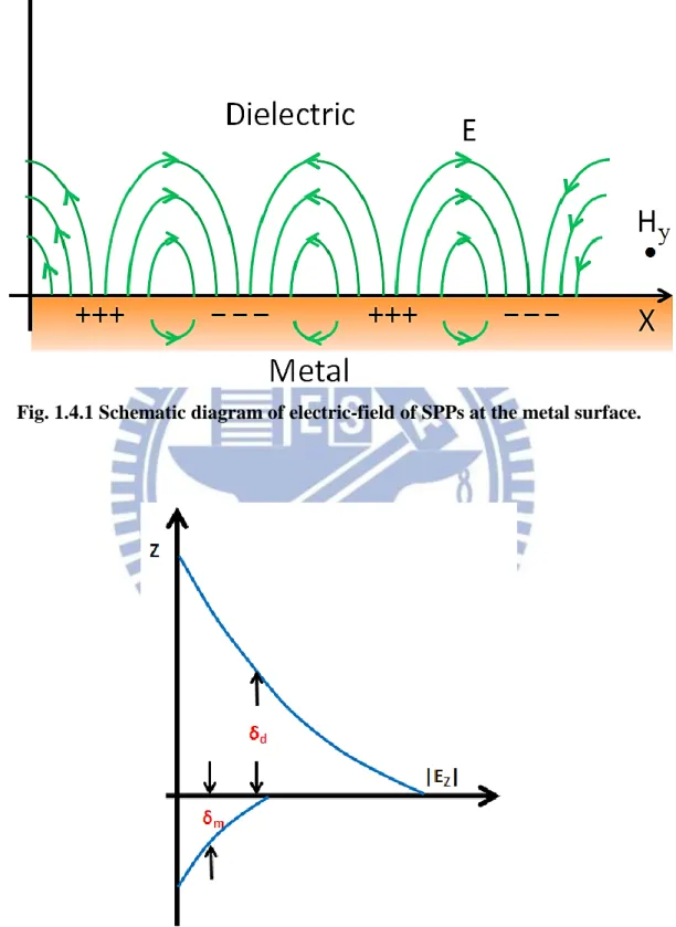
Fig. 1.4.1 Schematic diagram of electric-field of SPPs at the metal surface……… 12
Fig. 1.4.2 Electric-field distribution of SPPs at the metal/dielectric interface………. 12
Fig. 1.4.3 Applications of surface plasmon effect: (a) Biosensor (b) Lithography (c) Nanolaser……….. 13
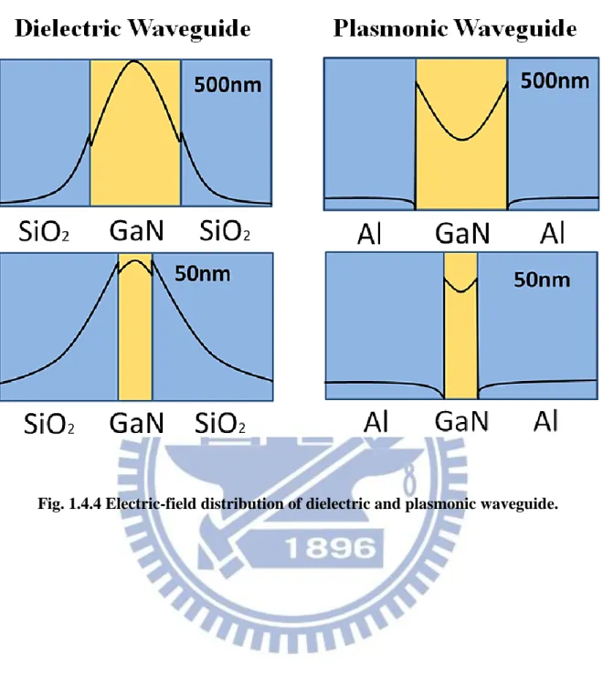
Fig. 1.4.4 Electric-field distribution of dielectric and plasmonic waveguide………..………. 14
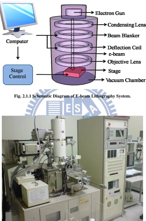
Fig. 2.1.1 Schematic Diagram of E-beam Lithography System………...………… 27
Fig. 2.1.2 ELX-7500 E-beam Lithography System……….…. 27
Fig. 2.3 Schematic Diagram of Micro-Photoluminescence System………. 30
Fig. 2.4 Process flow chart of metal-coated GaN grating structure……….. 30
Fig. 3.1.1 PL spectrum of undoped GaN………...41 Fig. 3.1.2 Intensity of electric-field mode profile through metal-coated grating structure…...41 Fig. 3.1.3 (a) Schematic diagram of the model used to optimize the grating structure (b)
wavelength and quality factor versus width of metal-coated grating structure
plot……… 42
Fig. 3.1.4 The wavelength and quality factor versus height of grating structure plot (a) Height from 80nm to 200nm, (b) Height from.200nm to 1000nm………... 43
Fig. 3.1.5 Simulated electric-field intensity through the metal-coated GaN grating
structure……….44
Fig. 3.1.6 The SEM image of grating structure in top view without metal-coated……...……44 Fig. 3.1.7 The SEM image of grating structure in angled view without metal-coated………. 45
Fig. 3.1.8 The SEM image of grating structure after deposition of dielectric and metal layer in angled view………... 45
Fig. 3.1.9 Schematic diagram of metal-coated GaN grating structure………..46 Fig. 3.2.1 PL spectrum of the metal-coated GaN grating structure below (black) and above
(red) threshold………... 46
Fig. 3.2.3 DOP of metal-coated GaN grating structure ( 96.5%)………..47 Fig. 4.2.1 Simulated electric-field intensity through the metal-coated GaN defect structure...60 Fig. 4.2.2 The SEM image of defect grating structure in top view without metal-coated….... 60
Fig. 4.2.3 The SEM image of defect grating structure in angle view without metal-coated… 61
Fig. 4.2.4 The SEM image of metal-coated defect grating structure in angle view…………..61 Fig. 4.2.4 Schematic diagram of metal-coated GaN defect grating structure………... 62
Fig. 4.3.1 PL spectrum of the metal-coated GaN defect grating structure below (black) and above (red) threshold……… 62
Fig. 4.3.2 Light-in light-out curves of defect lasing mode at 364nm………... 63
Fig. 3.2.3 DOP of metal-coated GaN defect grating structure ( 98.4%)………... 63
Fig. 4.4.1 Optical image of (a) Metal-coated GaN grating structure (b) Metal-coated GaN defect grating structure………..64 Fig. 4.4.2 Far-field angle of lasing mode of (a) Metal-coated GaN grating structure (b)
List of Symbols
θ:Angle of incidence λ:Wavelength of light wave 𝜆𝑠𝑝𝑝:Wavelength of the SPPs
𝑎:Periodicity of the grating structure
𝑘0:Wave vector component of the incident photon
𝑘𝑠𝑝𝑝:Wave vector component of the SPPs in the propagation direction 𝐿:The cavity length at the defect region
m:1,2,3,…
Chapter 1 Introduction
1.1 History of Laser
The concept of light amplification by the stimulated emission of radiation (LASER) should be traced back about one hundred years. In 1917, Albert Einstein first theoretically proposed the mechanism of stimulated emission which is the key process making laser action possible. After decades of researching laser, Theodore Maiman working at Hughes Aircraft Company invented the first functioning laser in the world in 1960. Although many historians claim that Theodore Maiman functioned the first laser; however, there is some controversy that the first optical laser was Gordon Gould invented. Maiman's ruby laser with the size of few centimeters was first operated on May 16, 1960 at Hughes Research Laboratories in California. Since then, the laser becomes the hot topic to study around the world.
Robert N. Hall who worked at General Electric in New York invented the first semiconductor laser in 1962. Not long ago, Nick Holonyak Jr. demonstrated first visible wavelength semiconductor laser in the same year lasing at 710nm [1]. Thereafter, many groups in the world contributed to the development of semiconductor laser. In 1992, S. L.
develop the applications of semiconductor laser in the near future. The semiconductor laser was first used for optical communication in fiber and then prompts the development of Internet slowly. Because many different materials can be used as the gain medium of the Laser Diodes (LDs), we can see many applications of semiconductor in our daily life like blue-ray disk for optical storage, or micro projector and laser television for display, even for medical and military purposes. Then, semiconductor laser gradually becomes one of the most important types of laser in the world.
The emitting wavelength of the first laser diode was designed at optical communication region with the gallium arsenide (GaAs) gain medium. Until now, there are many studies of semiconductor laser about indian gallium arsenide phosphorus (InGaAsP) material system with the lasing wavelength around visible or communicational wavelength region; however, there are only few studies about the ultraviolet (UV) lasers. So, the semiconductor laser of gallium nitride (GaN) material system with the lasing wavelength from visible to UV wavelength region has become a hot topic to study in the recent year. Fig. 1.1 shows the important invention in history of laser.
1.2 The Development of Metal-coated Nano Devices
In recent years, metal-coated cavity has been widely researched around the world. The size of semiconductor laser has shrunk by the metal-coated cavities from micro scale to
nanoscale, even in subwavelength region. The superiority of optical confinement and field enhancement due to the surface plasmon effects let metal-coated cavities break the diffraction limit size of laser [3]. In metal-coated cavity, the light penetrates little into the metal layer, but can be confined in a much smaller space which promise the nano devices lasing possible [4]. The lasing characteristics are intensely studies by scientists trying to figure out the physical meaning behind the experimental result.
In 2007, Hill et al. demonstrated the nanorod laser with the size far below its lasing wavelength [5]. They coated dielectric layer and silver layer on the nanorod device and observe the lasing signal in the communicational wavelength region at 77 K. After that, different designs of metal-coated nanostructure have reported in theory or experiment. K. Y. Yu et al. at 2010 demonstrated a nanopatch laser with metal-coated on the top and the bottom of the gain medium, and kept the effective mode volume and physical size of the nanopatch lasers at subwavelength scales [6]. In the same year, M. P. Nezhad et al. [7] demonstrated a metal-coated nanodisk with aluminum and SiO2 bi-layer shield surrounding an InGaAsP disk
and proposed a theoretical analysis to show that optimization of the dielectric layer. After optimizing process, they could have a higher chance to get a better quality factor laser and
difference between metal-coated device and no metal-coated device. Due to the combination of surface plasmon effect and whispering-gallery mode, metal-coated nanoring structure theoretically shows a possible way in demonstrating a high quality factor semiconductor laser even at the room temperature [9]. From recent research results [4-9], people use gold, silver, or aluminum to form the metal-coated nanostructure. Each kind of metals has the different absorption in different wavelength region and we should pick the one which had the lowest absorption at the wavelength of lasing peak. Table 1.2 shows some important results of metal-coated nano devices by researchers around the globe in recent years.
1.3 Application of GaN-based Optoelectronic Devices
GaN is a direct bandgap semiconductor material which has an advantage in radiative recombination than indirect bandgap material like silicon and gallium phosphorus. It has a wide bandgap (3.4 eV) property which makes it is superior for developing optoelectronic devices such as GaN-based Light Emitting Diodes (LEDs) and LDs, especially in blue or UV wavelength regions. Fig. 1.3 shows typical structures of GaN-based LDs and LEDs.
Since the invention of GaN-based LEDs, we can use the red, yellow and green phosphor material mixed with a blue or UV LED to make white light output possible. With the intensive development in manipulation of GaN material systems, the GaN-based LEDs become mature enough to create high brightness white LEDs in recent years [10-12]. And
background light of notebook and television, solid-state lighting and medical purposes. One day LEDs might replace the light bulb in the world due to the low consumption of energy. In the meanwhile, GaN-based semiconductor lasers have also intensively developed. In 1996, Nakamura et al. demonstrated the first GaN-based laser lasing at the room temperature continuous-wave (CW) condition [13] and established the fundamental of GaN-based laser. The technology of vertical-cavity surface emitting laser (VCSEL) is used in GaN materials and has been studied for many years [14-19]. VCSELs have some advantages including single-longitudinal-mode operation, two dimensional array capabilities and an emitted beam with a smaller angular divergence compared with edge emitting laser making a promise for designing high quality factor laser possible. The first VCSEL was presented in 1979 by Soda et al. [18], and the first devices which operated under CW operation condition at the room temperature were reported in 1988 [19]. In 2008, the GaN-based VCSELs were demonstrated by T. C. Lu et al operating at room temperature under CW condition [17]. Thanks to the intensive development in GaN-based VCSELs, many applications of its in our daily lives bring us very convenient environment, such as data transmission in optical fiber, laser printers, computer mouse and analysis of biological tissue.
1.4 Surface Plasmon Effect
Surface plasmon polaritons (SPPs) are light waves trapped on the interface of two materials which have the opposite sign on their real part of dielectric constant. The existence of SPPs can be attributed to resonant coupling of photons from the polarized light with the oscillation of metal free electron [20]. It is a kind of electromagnetic wave propagating along the surface of a conductor, usually in the metal-dielectric interface. SPPs propagate along the metal-dielectric interface have a combined electromagnetic wave and surface charge character as shown in Fig. 1.4.1. In Fig. 1.4.1, we can also see the generation of surface charge needs an electric-field perpendicular to the surface. The combined character of SPPs is increased near the surface and exponentially decaying with distance far away from it as shown in Fig. 1.4.2. The field δd means the decay length into dielectric layer or air and δm represents the decay
length into metal and we can also see that the field δm decreases to zero very soon for the
absorption problem in metal. Due to the electron gas couple with photons, the surface plasmon effect concentrate light under subwavelength scale even in few nanometers and make the laser with the size far below its lasing wavelength possible. One day SPPs might lead to miniaturized photonic circuits with unbelievable small size that we can imagine now. Nowadays, the surface plasmon effect is regarded much attention owing to the unknown phenomenon under such small scale.
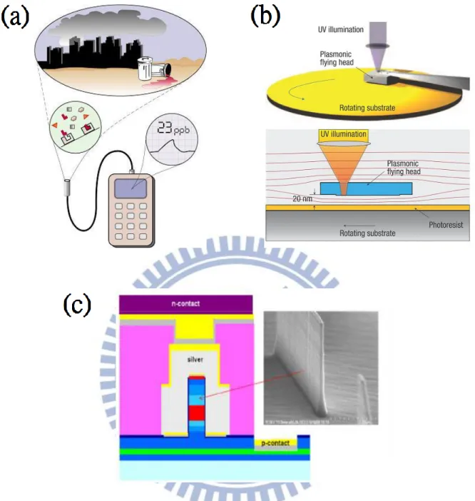
with nanometer scale. By changing the surface structure of the metal, the wavelength of light interacting in the dielectric/metal interface is tunable, which offers the huge potential for developing new types of photonic device [20]. Thanks to lots of research in SPPs, we have more and more specific applications of SPPs in our daily lives [5, 20-22]. For instance, SPPs is used to make sensors which is called biosensor for observing the activity of biomolecules. There are other applications like magneto-optic data storage, advanced lithography technique [22], LED, nanolaser and nanophotonic applications [23]. Fig. 1.4.3 shows some applications of surface plasmon effect. Many years ago, it was difficult to observe the behavior of a biomolecule for researchers. But now, researchers can utilize surface plasmon effect to improve the extraction of light and make it is possible to observe the biomolecule even in only few nanometers. With the invention of this new technique, researchers could observe unknown phenomena in biomolecules and analyze it. This technology has been applied to medical proposed like drug screening, kinase analysis and research on antibody development [21].
Fig. 1.4.4 shows the distribution of optical field for dielectric and plasmonic waveguide structures. The maximum intensity of dielectric waveguide mode is at the middle of the GaN
By taking the advantages of surface plasmon effect, W. Srituravanich et al. report a maskless nanolithography technique with low-cost and high-throughput characteristic and experimentally demonstrated the patterned device with a linewidth of only 80 nm [22]. After this new invention has been reported, the nanolithography becomes mature enough to fabricate the nano devices and let many researches achieve a semiconductor laser in subwavelength scale [5]. In recent years, there are many reports about using different metals and cavities have been proposed by some research groups. This will discuss later in the following section in details.
1.5 Motivation
For many advantages of metal-coated nanocavity, the size of semiconductor laser could be shrunk into subwavelength scale. If we properly design the cavity well, the propagating SPPs can also be localized in it theoretically [24]. By now, there are many research results of semiconductor laser mainly focus on InGaAsP material system with the lasing wavelength around infra-red or communicational wavelength region; however, the study about UV semiconductor laser is seldom reported in the world. Therefore, we want to use the surface plasmon effect and the GaN material to design the UV laser with low threshold power density and high quality factor. Although there is a momentum mismatch problem between light and the SPP in surface plasmon effect, we can use grating structure to solve this issue [25].
In this thesis, we use GaN as the gain medium coating with silicon nitride (Si3N4) and
aluminum layer to form the metal-coated cavity and discuss the experimental lasing results compared with the simulation. We utilize some manufacturing methods to demonstrate our device, like E-beam lithography, plasma-enhanced chemical vapor deposition (PECVD), inductively coupled plasma reactive ion etching (ICP-RIE) and E-gun evaporation.
In chapter 2, we briefly introduce the manufacturing instruments which are used to fabricate the device and measure its characteristics. Then in chapter 3, we design and optimize the metal-coated GaN grating structures device and analyze the lasing characteristics of it. Then, we will discuss the experiment result with effective refractive index method. In chapter 4, we destruct the periodic characteristic of the grating structures and design a defect pattern in the grating structure. We expect the lights will concentrate in the defect pattern and the threshold power density of it will much lower than the grating structure device. Finally, we will give a brief summary of this thesis in chapter 5.
Fig. 1.1 The important invention in history of LASER.
Fig. 1.4.1 Schematic diagram of electric-field of SPPs at the metal surface.
Fig. 1.4.3 Applications of surface plasmon effect: (a) Biosensor (b) Lithography (c) Nanolaser.
References
[1] N. Holonyak and S. F. Bevacqua, “Coherent (visible) light emission from Ga(As1−xPx)
Junctions,” Appl. Phys. Lett. 1, 82 (1962).
[2] S. L. McCall, A. F. J. Levi, R. E. Slusher, S. J. Pearton, and R. A. Logan, “Whispering-gallery mode microdisk lasers,” Appl. Phys. Lett. 60, 289 (1992).
[3] C. Z. Ning, “Semiconductor nanolasers,” Phys. Status Solidi B 247, 774 (2010).
[4] M. W. Kim and P. C. Ku, “Lasing in metal-clad microring resonator,” Appl. Phys. Lett. 98, 131107 (2011).
[5] M. T. Hill, Y. S. Oei, B. Smallbrugge, Y. Zhu, T. de Vries, P. J. van Veldhoven, F. W. M. van Otten, T. J. Eijkemans, J. P. Turkiewicz, H. de Waardt, E. J. Geluk, S. H. Kwon, Y. H. Lee, R. Nötzel, and M. K. Smit, “Lasing in metallic-coated nanocavities,” Nat. Photonics
1, 589 (2007).
[6] K. Yu, A. Lakhani, and M.C. Wu, “Subwavelength metal-optic semiconductor nanopatch lasers,” Opt. Express 18, 8790 (2010)
[7] M. P. Nezhad, A. Simic, O. Bondarenko, B. Slutsky, A. Mizrahi, L. Feng, V. Lomakin, and Y. Fainman, “Room-temperature subwavelength metallo-dielectric lasers,” Nat. Photonics,
[9] Y. G. Wang, S. W. Chang, C. C. Chen, C. H. Chiu, M. Y. Kuo, M. H. Shih, and H. C. Kuo, “Room temperature lasing with high group index in metal-coated GaN nanoring, ” Appl.
Phys. Lett. 99, 251111 (2011).
[10] S. Nakamura, M. Senoh, N. Iwasa, and S. Nagahama, “High-brightness InGaN blue, green, and yellow light-emitting diodes with quantum well structures,” Jpn. J. Appl. Phys.
34, L797 (1995).
[11] M. H. Kim, M. F. Schubert, Q. Dai, J. K. Kim, E. F. Schubert, J. Piprek, and Y. Park, “Origin of efficiency droop in GaN-based light-emitting diodes,” Appl. Phys. Lett. 91,
183507 (2007).
[12] C. H. Wang, S. P. Chang, W. T. Chang, J. C. Li, Y. S. Lu, Z. Y. Li, H. C. Yang, H. C. Kuo, T. C. Lu, and S. C. Wang, “Efficiency droop alleviation in InGaN/GaN light-emitting
diodes by graded-thickness multiple quantum wells,” Appl. Phys. Lett. 97, 181101 (2010).
[13] S. Nakamura, M. Senoh, S. Nagahama, N. Iwasa, T. Yamada, T. Matsushita, Y. Sugimoto, and H. Kiyoku, “Room-temperature continuous-wave operation of InGaN
multi-quantum-well structure laser diodes,” Appl. Phys. Lett. 69, 4056 (1996)
[14] J. T. Chu, T. C. Lu, H. H. Yao, C. C. Kao, W. D. Liang, J. Y. Tsai, H. C. Kuo, and S. C. Wang, “Room-temperature operation of optically pumped blue-violet GaN-based
2556 (2006).
[15] C. C. Kao, T. C. Lu, H. W. Huang, J. T. Chu, Y. C. Peng, H. H. Yao, J. Y. Tsai, T. T. Kao, H. C. Kuo, S. C. Wang, and C. F. Lin, “The lasing characteristics of GaN-based
vertical-cavity surface-emitting laser with AlN/GaN and Ta2O5/SiO2 distributed bragg
reflectors,” IEEE Photonics Tech. Lett. 18, 877 (2006).
[16] P. C. Peng , H. C. Kuo , W. K. Tsai , Y. H. Chang , C. T. Lin , S. Chi , S. C. Wang, G. Lin, H. P. Yang,K. F. Lin, H. C. Yu, and J. Y. Chi, “Dynamic characteristics of long-wavelength quantum dot vertical-cavity surface-emitting lasers with light injection,” Opt. Express 14, 2944 (2006).
[17] T. C. Lu, C. C. Kao, H. C. Kuo, G. S. Huang, and S. C. Wang, “CW lasing of current injection blue GaN-based vertical cavity surface emitting laser,” Appl. Phys. Lett. 92, 141102 (2008).
[18] H. Soda, K. Iga, C. Kitahara, and Y. Suematsu, “GaInAsP/InP surface emitting injection lasers,” Jpn. J. Appl. Phys. 18, 2329 (1979).
[19] F. Koyama, S. Kinoshita, K. Iga, “Room temperature CW operation of GaAs vertical cavity surface emitting laser,” IEICE Trans. E71-E, 1089 (1988).
plasmon resonance biosensors: a review of recent progress,” Biosens Bioelectron. 23, 151 (2007).
[22] W. Srituravanich, L. Pan, Y. Wang, C. Sun, D. B. Bogy, and X. Zhang, “Flying plasmonic lens in the near field for high-speed nanolithography,” Nat. Nanotechnology 3, 733 (2008).
[23] H. J. Lezec, J. A. Dionne, and H. A. Atwater, “Negative refraction at visible frequencies,” Science 316, 430 (2007).
[24] Y. Gong and J. Vučković, “Design of plasmon cavities for solid-state cavity quantum electrodynamics applications,” Appl. Phys. Lett. 90, 033113 (2007).
[25] R. H. Ritchie, E. T. Arakawa, J. J. Cowan, and R. N. Hamm, “Surface-plasmon resonance effect in grating diffraction,” Phys. Rev. Lett. 21, 1530 (1968).
Chapter 2 Experimental Instruments and Methods
2.1 Electron Beam Lithography and Scanning Electron Microscope (SEM)
Electron Beam Lithography System
Electron beam (E-beam) lithography is a technique to use the electron beam to expose the photo resist on the surface of sample with the designed pattern, and then we can fix the pattern on the photo resist layer by selectively removing the photo resist. The E-beam lithography system usually consists of an electron gun as source of electron, lenses for focusing, stage for moving the sample precisely, a beam blanker to control the exposure time of electron beam and a computer to control the whole system. Fig. 2.1.1 shows the schematic diagram.
This method could break the diffraction limit which is constrained by conventional photo lithography technique, and makes a promise for fabricating device in subwavelength scale. However, most of E-beam lithography system used for commercial applications are very expensive; therefore, in order to cost down the E-beam lithography system, people usually convert an electron microscope which is also an expensive machine into an E-beam lithography system with a relatively low cost especially for academic purpose. For thesis, we
Scanning Electron Microscope
Scanning electron microscope (SEM) is the very important equipment for people to observe the pattern which is on objects in microscale or nanoscale. The electrons interact with atoms of the object that make up the sample producing signals contained information about itself. The electron beam is focused by one or two condenser lenses to a spot with the size about 0.4 nm to 5 nm in diameter. The preparation of the samples for SEM is easy due to the fact that SEM only require the sample with good conductivity. The combination of higher magnification, larger depth of focus, greater resolution, and ease of sample observation makes the SEM becomes one of the most widely used equipment used for commercial and research purposes. Fig. 2.1.3 shows the JSM-7000F made by JEOL.
2.2 Dry Etching Process and E-gun Evaporation
Dry Etching Process
Dry etching process is critical for scientists to fabricate the device according to their plan, and there are two types of etching processes: wet etching and dry etching. Dry etching process uses plasma to etch the semiconductor material and it is a kind of anisotropic etching process. The linewidth of dry etching process is smaller than wet etching, therefore, dry etching process gradually replace wet etching process after 1980.
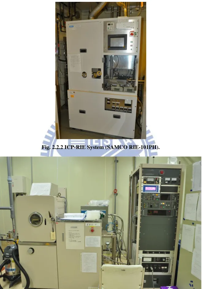
diffuse to chamber under ultra-low pressure. Second, when the pressure is stable, plasma is produced by RF frequency. Third, the radicals produced by bombardment of high speed electron would diffuse to the wafer and attach to its surface. Fourth, with the help of ion bombardment, these radicals would react with the atoms on the surface and form by-product as gas. At the end, these volatile by-products would then leave the surface of wafer and discharge from chamber. Fig. 2.2.1 shows the inductively coupled plasma and reactive ion etching (ICP-RIE) system used to etch Si3N4 layer to transfer the patter from PMMA layer,
and Fig. 2.2.2 shows the ICP-RIE equipment used to etch GaN layer.
E-gun Evaporation
E-gun evaporation, also called as E-beam evaporation, is one kind of physical vapor deposition (PVD). The difference of E-gun evaporation is that it uses electron beam to heat up the source material. The advantage of E-gun evaporation is that it could heat only one small part of the surface of the source material. This will reduce the energy consumption used by PVD. Therefore, it is a common way to use E-gun evaporation to deposit metal on to the device. For an E-gun evaporation system, it consists of an electron beam evaporation gun, a
2.3 Micro-Photoluminescence (μ-PL) System
Micro-Photoluminescence is an advanced Photoluminescence system to measure sample in micrometer even nanometer scale. The spot size of the light source for μ-PL system has shrunk to micrometer scale to observe the optical properties of sample. In our μ-PL system, we use Nd:YVO4 laser with lasing wavelength 355nm as a pumping source, and the
spot size is about 50μm, frequency of the laser is 1kHz, and the pulse width is about 500ps. The schematic diagram of μ-PL system is shown in Fig. 2.3.
2.4 Fabrication Process of Metal- coated GaN Grating Structures
We use the 2 μm thick undoped GaN as the gain medium of grating structure laser, which is grown on a c-plane (0001) sapphire substrate by metal-organic chemical vapor deposition (MOCVD) system (EMCORE D-75). We use Trimethygallium (TMGa) and Ammonia (NH3) as the gallium and nitride sources respectively. A thermal cleaning process is
carried out at 1080℃ for 10 minutes in a stream of hydrogen ambient before the growth of epitaxial layers to clean the sample surface. Then, the 30nm thick GaN nucleation layer is first grown on the sapphire substrate at 530℃, and at the end the 2μm thick undoped GaN layer is grown on it at 1040℃.
After the undoped sample is prepared, the 200 nm thick Si3N4 is deposited on the
(PECVD). After that, we coat the 250nm polymethylmethacrylate (PMMA) on Si3N4 by
spin-coating method. We define the grating pattern on the PMMA layer by E-beam lithography, then using reactive ion etching (RIE) with CHF3/O2 mixture to etch down to the
Si3N4 layer. Next, we transfer the grating pattern from Si3N4 layer to the undoped GaN layer
to form the grating structure with about 200nm depth by inductively coupled plasma reactive ion etching (ICP-RIE) with Cl2 /Ar mixture. The Si3N4 mask layers are removed by wet
etching after all above processes. Before we begin to do the next step, we clean our sample by wet etching methods, washing away the particles created in the previous dry etching processes to promote the performance of our device. To improve the quality factor of the device, we deposit 30nm Si3N4 layer on the patterned GaN layer. After that, a 50 nm aluminum layer is
coated on the device by E-gun evaporation to form the grating structure of metal-coated GaN laser.
The dry etching processes may cause the surface roughness of the device, but the Si3N4
would passive this roughness when we coat the dielectric layer on the grating structure. The surface roughness will generate the nonradiative center on the surface of grating structure reducing the performance of device. The Si3N4 layer between the metal and GaN will reduce
and the process flow chart of metal-coated GaN grating structure is shown in Fig. 2.4 PECVD (SAMCO PD220) Si3N4 film deposition: SiH4 /Ar:20sccm NH3:10sccm N2:490sccm Temperature:300℃ RF power:35W Pressure:100Pa Deposition rate:9.6nm/min
ICP-RIE (Oxford Plasmalab System 100)
Si3N4 film etching: Ar/O2: 5sccm CHF3:50sccm RF power:150W Pressure:7.5×10⁻⁹ Torr Temperature:20℃ Etching rate:81.7nm/min
ICP-RIE (SAMCO RIE-101PH)
GaN film etching:
Cl2:25sccm Ar:10sccm ICP power:200W Bias power:200W Pressure:0.33Pa Etching rate:545nm/min
E-beam Lithography System (JEOL JSM-6500)
Spin coating use PMMA (A5)
Spinning rate in first step:1000 rpm (10sec) Spinning rate in second step:3500 rpm (25sec) Hard bake:
Temperature:180℃ (90sec) Exposure:
Development:
MIBK:IPA (1:3) :70sec Fixing:
IPA:40sec
E-gun Evaporation System (ULVAC EBX-8C)
Source:Aluminum
Pressure:3×10 -6 Torr
Current:170mA for first 5nm 190mA for the rest 45nm
Fig. 2.1.3 JSM-7000F SEM System.
Fig. 2.3 Schematic Diagram of Micro-Photoluminescence System.
References
[1] A. Mizrahi, V. Lomakin, B. A. Slutsky, M. P. Nezhad, L. Feng, and Y. Fainman, “Low threshold gain metal coated laser nanoresonators,” Opt. Lett. 33, 1261 (2008).
Chapter 3 Band Edge Mode Lasing in Metal-coated GaN Grating
Structure at Room Temperature
3.1 Design and Optimize the Device
Photonic crystals are regarded much attention owing to their photonic band structure recently [1]. Light at the band edge of one dimensional photonic bandgap has nearly zero group velocity and forms a standing wave which makes the laser action possible. The uniformed grating structure would form the plasmonic bandgap and we can observe the band edge mode from it theoretically. By combining the advantages of the metal-coated cavities and the structure of one dimensional photonic crystal like grating structure, we can obtain single-mode output and high quality factor laser possible. A grating structure with uniformed periodicity can be used to couple light to the SPPs. The SPPs exist at a specific condition which is needed to satisfy the following equation [2]:
𝑘𝑠𝑝𝑝 = 𝑛𝑒𝑓𝑓𝑘0 = 𝑘0 sin(𝜃) ± m2𝜋𝑎 (1)
The peak of emission wavelength of GaN is about 365nm which can be speculated from the bandgap of GaN (3.4eV). The Fig. 3.1.1 shows the Photoluminescence (PL) spectrum of undoped GaN layer and we can find that the emission wavelength range of GaN is from 360nm to 380nm. Therefore, we use the FEM to design the metal-coated GaN grating structure with the high quality factor at about 370nm.
undoped GaN and sapphire. The refractive indices of aluminum and undoped GaN layers are established by Palik [3] and Peng et al [4]. We also set a perfectly matched layer at the bottom of GaN to absorb redundant signal which might reflect back to the metal-coated grating structure and use the 50nm metal layer and 30nm dielectric layer which is referred from report [5] to simulate the electric-field mode profile in it. Finally, we find a band edge mode in the designed structure. Fig. 3.1.2 shows the simulated electric-field intensity plot through the metal-coated GaN grating structure. By using FEM, we can see that the SPPs clearly exist in the metal-coated GaN grating structure from Fig. 3.1.2 with wavelength of 369.5 nm and the quality factor of it is estimated about 200. Then, we fix the period of this structure which is 840nm and further optimize the height and width of it to get the higher quality factor laser. The higher quality factor represented the longer average lifetime of resonant photons in the cavity and result in better performance of laser. Fig. 3.1.3 (a) shows schematic diagram of the model used to optimize the metal-coated GaN grating structure. Fig. 3.1.3 (b) is the quality factor versus width of grating structure plot, and we find the best width of it is about 220nm. Afterwards, we fix the period and width of the grating structure and tune the height of it to achieve the best performance in our device. We find the best height of this structure is about
will find that the wavelength of Fig. 3.1.3 (b) and Fig. 3.1.4 (a) increase with increasing the width or height of grating structure.
In Fig. 3.1.4 (a), the height of grating structure which we use to simulate by FEM is from 130 to 250nm. If we continually simulate the height of grating structure from 250nm to 1000nm, we will find the highest quality factor which appears when the height of it is about 900nm as shown in Fig. 3.1.4 (b). However, there is dielectric mode dominate when the height of grating structure is about 900nm and the SPPs is even difficult to find in grating structure as shown in Fig. 3.1.5. For further design the defect mode in grating structure which has the advantage of low threshold power density in chapter 4, it should be depended on surface plasmon effect to achieve [6]. We examine the electric-field mode profile in each height of grating structure by FEM, and find the SPPs clearly exist below the height of it which is approximately 250nm. Therefore, we should demonstrate the grating structure which the height of it is below 250nm first and measure the lasing characteristic to confirm the device is functional. Then, we start to demonstrate the grating structure which the period, width and height of it are 840nm, 220nm and 180nm respectively. The width and height of this structure are both below the wavelength of the expected lasing mode. We also design it with the field size of 50μm×50μm, because the diameter of laser spot size used to pump device is approximately 50μm.
processes are finished, we use SEM to check the size of grating structure and make sure the period, width and height of it is what we want. Fig. 3.1.6 and Fig. 3.1.7 show the SEM image of grating structure in top view and angled view without metal-coated respectively. The period, width and height of it are 840nm, 220nm and 150nm respectively. Although, the height of it is not 180nm which has the best quality factor, we can see that grating structure has not bad quality factor when the height of it is 150nm from Fig. 3.1.4 (a). The SEM image of grating structure after deposition of dielectric and metal layer is shown in Fig. 3.1.8 in angled view, and the schematic diagram of metal-coated GaN grating structure is shown in Fig. 3.1.9.
3.2 Lasing Characteristics of Band Edge Mode in Metal-coated GaN Grating Structure
We use the μ-PL system which is mentioned in chapter 2 to measure the characteristics of the device. The grating structure of metal-coated GaN layer was optically pumped by a frequency-tripled Nd:YVO4 355 nm pulsed laser at room temperature. A 15×objective lens is
used to collect the lasing signal from the grating structure laser through a multimode fiber, and couple into a spectrometer with the charge-coupled device detectors. We optically pump our device from the metal-coated surface, because the bulk GaN layer beneath the surface of
and above (red) the threshold power density. We can see a clearly single lasing mode at 368nm from Fig. 3.2.1 and observe the difference between the curve of below and above the threshold power density which ensure a lasing action in the grating structure. Fig. 3.2.2 shows the light-in light-out curves of this mode and the linewidth of the lasing mode above the power density is about 0.53nm. When the power density is above 19W/cm2, we observe the linear behavior in Fig. 3.2.2 which indicates the lasing action, and also find that the linewidth is narrowing. The narrowing linewidth shows that the emission mechanism in GaN is from spontaneous emission to stimulated emission. These evidences prove the lasing action in our metal-coated GaN grating structure. The steady blue-shift behavior as pumping power increase in Fig. 3.2.2 indicates that the performance of device is less influenced by heat effect even operating at high power density due to the good thermal dissipation of metal. The threshold power density of the grating structure is about 19W/cm2 and the quality factor estimated by the wavelength to linewidth around the transparency is 570. Next, we measure the degree of polarization (DOP) of metal-coated GaN grating structure. In Fig. 3.2.3, the DOP is about 96.5%, and the strongest intensity of it is occurred when the polarizer is perpendicular to the grating. The high DOP shows the good linear performance of our device.
To ensure that the lasing action is accurately originated from our grating structure, we use a Nd:YVO4 laser to pump the flat and grating structure region of undoped GaN layer and
3.2.4, the peak wavelength of the flat and grating structure region of undoped GaN layer are all about 366nm and no lasing signal is observed. However, the spectrum of the flat region of metal-coated GaN layer is totally different compared to undoped GaN layer without metal-coated. The peak wavelength of undoped GaN around 366nm no longer exists because the energy from 360nm to 380nm had been almost absorbed by metal layer. Therefore, we confirm that the lasing action is truly from grating structure.
3.3 Results and Discussion
The lasing wavelength of metal-coated GaN grating structure may cause a little difference between experimental and simulation results. This is attributed to the imprecise size of device observed from SEM, uncertainty in the fabrication process, small error of material indices used in the simulation model and the slight edge roughness of the device. To check the reason why the GaN grating structure without metal-coated is not a functional laser, we use FEM to simulate the optical mode in GaN grating structure without metal-coated. Fig. 3.3.1 shows the quality factor versus wavelength of it and we find that the quality factor of all optical modes are very low around the emission wavelength of GaN. Fig. 3.3.2 shows the best
grating structure is very weak from Fig. 3.3.2. The quality factor of the optical mode shown in Fig. 3.3.2 is about 25 which is eight times smaller than the case in Fig. 3.1.2. All these results indicate that the GaN grating structure without metal-coated is barely possible lasing in low pump power density that is why we cannot observe the laser action in GaN grating structure without metal-coated.
Compared with silver, aluminum has a higher reflectivity at UV wavelength region which could show a better optical confinement [7]. The absorption of aluminum at UV wavelength region is also smaller than silver and gold. Moreover, aluminum has the better adhesion to Si3N4 than gold. Hence, we use aluminum instead of other metal like silver or
gold to coat on grating structure. From the thermal conductivity of aluminum (237W/m·K) which is thousand times than air (0.025W/m·K), it shows that metal-coated GaN grating structure has more opportunity to observe lasing action than the uncoated one before the device burn out. We think the advantage of the high thermal conductivity and high reflectivity of aluminum increase the lasing possibility even at room temperature. Table 3.3 lists a comparison between nanostripe [8] and grating structure. As shown in the Table 3.3, the quality factor has improved significantly which is about four times larger than nanostripe. Moreover, the threshold power density of grating structure is much lower than nanostripe. We believe that the utilization of SPPs would be the critical reason for these results.
structure. In the beginning, we split the period grating structure into two parts: the stripe part and pitch part. This way will put the two dimensional structure into one dimension to simulate which is easy for calculation and also keeps the high accurate result. Then, we plot the band diagram of the grating device to match the FEM simulation result and estimate the effective refractive index of each part as shown in Fig. 3.3.3. A schematic diagram of the model used in effective refractive index method is shown in Fig. 3.3.4. The estimated effective refractive index of grating structure under transverse electric (TE) mode is shown in Fig. 3.3.5. The effective index of stripe part is 2.605 and the pitch part is 2.6117. Because the effective refractive index of both of them are between the air (n=1) and GaN (n=2.71), we can say the simulation result is reasonable and believe that it is the band edge mode lasing in the metal-coated GaN grating structure.
In the FEM simulation result, we observe that the part energy of electric-field would loss at the bottom of GaN. If we can further improve the vertical confinement in our device, the performance of it will have impressive result. Distributed Bragg Reflector (DBR) might be the one way to significantly reduce this problem. In 2010, C. Y. Lu et al. demonstrated metal-coated microrod with an n-type DBR lasing under room temperature CW operation
3.4 Summary
In summary, we successfully demonstrate the band edge laser with the lasing wavelength around 368 nm. The period, width and height of the metal-coated GaN grating structure are 840nm, 220nm and 150nm respectively. The lasing action from a metal-coated GaN grating structure at room temperature with a high quality factor of 570 and the threshold power density of 19W/cm2 is observed. The FEM simulation result showed the importance of aluminum layer and the lasing evidence of the metal-coated GaN grating structure. From the effective refractive index method simulation result, we confirm that the lasing action of grating device is attributed to the band edge mode. From experimental and simulation results, the grating structure without metal-coated is difficult to achieve lasing action at room temperature due to the poor optical confinement and the terrible thermal conductivity by air even make it lasing impossible under low pump power density. The advantage of band edge mode let us observe the single-mode lasing action which has the huge potential for developing high quality nanolaser in the future.
360
370
380
390
400
410
0.0
0.2
0.4
0.6
0.8
1.0
Int
ensit
y (
a.u.)
Wavelength (nm)
Fig. 3.1.1 PL spectrum of undoped GaN.
200 210 220 230 240 250 260
350
360
370
380
390
Width (nm)
Wavele
n
gth
(n
m)
0
50
100
150
200
250
Q
ual
it
y f
actor
Fig. 3.1.3 (a) Schematic diagram of the model used to optimize the grating structure
120 140 160 180 200 220 240 260
360
370
380
390
Height (nm)
Wav
elength (nm
)
50
100
150
200
250
Q
ual
it
y f
actor
200
400
600
800
1000
360
370
380
390
400
Height (nm)
Wav
elength (nm
)
50
100
150
200
250
300
Q
ual
it
y f
actor
Fig. 3.1.5 Simulated electric-field intensity through the metal-coated GaN grating structure at 395nm with quality factor about 250. The period, width and height of it are
840nm, 220nm and 900nm respectively.
Fig. 3.1.9 Schematic diagram of metal-coated GaN grating structure.
360
370
380
390
400
410
0.0
0.2
0.4
0.6
0.8
1.0
10 W/cm
221 W/cm
2Int
ensit
y (
a.u.)
Wavelength (nm)
Fig. 3.2.1 PL spectrum of the metal-coated GaN grating structure below (black) and above (red) threshold.
0
5
10
15
20
25
0.0
0.2
0.4
0.6
0.8
1.0
Pump Power Density
(
W/cm
2
)
Int
ensit
y (
a.u.)
0.50
0.55
0.60
0.65
0.70
0.75
Li
newi
dt
h (
nm
)
Fig. 3.2.2 Light-in light-out curves of band edge lasing mode.
0.0
0.2
0.4
0.6
0.8
1.0
-150 -140 -130 -120 -110 -100 -90 -80 -70 -60 -50 -40 -30 -20 -10 0 10 20 30 40 50 60 70 80 90 100 110 120 130 140 1500.0
0.2
0.4
0.6
0.8
1.0
360
370
380
390
400
410
0.0
0.2
0.4
0.6
0.8
1.0
Int
ensit
y (
a.u.)
Wavelength (nm)
Plane GaN
Plane metal-coated GaN
GaN grating structure
without metal-coated
Fig. 3.2.4 PL Spectrum of the plane region of metal-coated GaN and the GaN grating structure with and without metal and dielectric layers.
365
370
375
380
385
390
0
10
20
30
40
50
Q
ual
it
y f
actor
Wavelength (nm)
Fig. 3.3.1 The quality factor versus wavelength of GaN grating structure without metal-coated plot.
Fig. 3.3.2 Simulated electric-field intensity through the metal-coated GaN grating structure at 384.6nm with quality factor about 25.
Fig. 3.3.4 Schematic diagram of the model used in effective refractive index method.
References
[1] S. Noda, A. Chutinan, and M. Imada, “Trapping and emission of photons by a single defect in a photonic bandgap structure,” Nature 407, 608 (2000).
[2] Maier and A. Stefan, “Plasmonics: fundamentals and applications,” Springer (2007). [3] Edward D. Palik, “Handbook of Optical Constants of Solids,” Academic Press (1997). [4] T. Peng and J. Piprek, “Refractive index of AlGaInN alloys,” Electron. Lett. 32, 2285
(1996).
[5] M. P. Nezhad, A. Simic, O. Bondarenko, B. Slutsky, A. Mizrahi, L. Feng, V. Lomakin, and Y. Fainman, “Room-temperature subwavelength metallo-dielectric lasers,” Nat. Photonics
4, 395 (2010).
[6] A. Kocabas, S. S. Senlik, and A. Aydinli, “Plasmonic band gap cavities on biharmonic gratings,” Phys. Rev. B 77, 195130 (2008).
[7] W. M. Rohsenow and H. Y. Choi, “Heat mass and momentum transfer,” Prentice-Hall (1961).
[8] Y. G. Wang, C. C. Chen, C. H. Chiu, M. Y. Kuo, M. H. Shih, and H. C. Kuo, “ Lasing in metal-coated GaN nanostripe at room temperature,” Appl. Phys. Lett. 98, 131110 (2011). [9] C. Y. Lu, S. W. Chang, S. L. Chuang, T. D. Germann, and D. Bimberg, “Metal-cavity
surface-emitting microlaser at room temperature,” Appl. Phys. Lett. 96, 251101 (2010). [10] M. T. Hill, “Status and prospects for metallic and plasmonic nano-lasers,” J. Opt. Soc.
Chapter 4 Defect Mode Lasing at the Defect of Metal-coated GaN Grating
Structure at Room Temperature
4.1 Introduction
We observe the band edge mode lasing in the metal-coated GaN grating structure due the SPPs effect and confirm the bandgap behavior of grating structure from chapter 3. If we further destruct the periodic characteristic of the grating structures, we would make a defect mode laser with threshold gain which is far below the band edge laser. The perturbation of effective refractive index contrast between the defect and its surroundings lead to an extra phase change in the propagating waves and result in a constructive interference at a specific wavelength which is called cavity mode or defect mode [1]. Photons propagating through the waveguide structure are trapped by the defect which then emits them to free space, and this kind of phenomenon would be used in ultra-small optical devices in the future [2].
The capability to control the effective refractive index of grating structure enables the fabrication of plasmonic cavity in it possible. If we selectively change the index of the grating structure, the optical properties of SPPs will be perturbed and form a defect mode in it. In this thesis, we employ grating structure to couple to the SPPs first which is demonstrated in
4.2 Design the Device
SPPs with a forbidden wavelength which is in previously grating structure can still propagate if the following resonance condition is met [3]:
𝐿 = (2m + 1)𝜆𝑠𝑝𝑝
4 (2)
We need to design the proper cavity length at defect region (L). From the FEM, we know the wavelengths at the bandgap of metal-coated grating structure are 363nm and 369nm. The effective refractive index of stripe part of the metal-coated grating structure is 2.6805 as discussed in chapter 3. We assume the wavelength of defect mode is 365nm which is between 363nm and 369nm. Therefore, we can get that the value of 𝜆𝑠𝑝𝑝 is 136.16nm approximately. Then, we set the value of m to be 4 and finally estimate that the cavity length at defect region (L) is around 306nm.
We use FEM to check the existence of defect mode and successfully find a defect mode in it as shown in Fig. 4.2.1. The condition of simulation and the height, width and period of grating structure are same as in chapter 3, with the exception of defect region. Fig. 4.2.1 shows the simulated electric-field intensity plot through the metal-coated GaN defect grating structure and the cavity length at defect region is about 300nm which is closed to the value what we calculate. We can see that the defect mode clearly exist in the middle of grating structure from Fig. 4.2.1 with wavelength of 365 nm and the quality factor is estimated about 160.
The FEM simulation result shows a promising chance to demonstrate the defect mode laser. Therefore, we start to fabricate the defect grating structure which the period, width and height of it are 840nm, 220nm and 180nm respectively, and the cavity length of defect region is 300nm. We also design it with the field size of 50μm×50μm based on the diameter of laser spot size used to pump device. After the fabrication processes mentioned in chapter 2.4 are finished, we use SEM to observe the period, width and height of defect grating structure. The SEM image of defect grating structure in top view and angled view without metal-coated are shown in Fig. 4.2.2 and Fig. 4.2.3 respectively. The cavity length of defect region of it is about 305nm and the period, width and height of it are 840nm, 220nm and 160nm respectively. Fig. 4.2.4 shows the SEM image of defect grating structure after deposition of dielectric layer and 50nm Al in angled view, and the schematic diagram of metal-coated GaN defect grating structure is shown in Fig. 4.2.5.
4.3 Lasing Characteristics of Defect Mode in Metal-coated GaN Grating Structure
To measure the lasing characteristics of the device we use the μ-PL system which is mentioned in chapter 2 with room temperature condition. In order to avoid absorption losses
density and the difference between two curves indicate a lasing action in it with lasing wavelength around 364nm.
The threshold pump power density is 4.6W/cm2 which is obtained from the experimental result as shown in Fig. 4.3.2 and the linewidth of the lasing mode above the power density is about 0.75nm. The quality factor estimated by the ratio of wavelength to linewidth around the transparency is about 480. Then, we measure the DOP of metal-coated GaN defect grating structure. In Fig. 4.3.3, the DOP is about 98.4% which is similar to grating structure as mentioned in chapter 3.
4.4 Results and Discussion
At the metal-coated defect grating device, the SPPs though in the grating structure is centralized in the defect region with high photons concentration and this result will increase the absorption in metal compared to the one without defect designed. Therefore, we can see that the quality factor of defect structure is smaller than the metal-coated grating structure in experiment and FEM simulation result.
Compare to the grating structure, defect grating structure has a unique advantage that SPPs highly concentrate in small region [1]. Therefore, we speculate that metal-coated GaN defect grating structure metal would have the lasing possibility at room temperature under ultra-low pump power density and confirms our hypothesis from the experiment result. Table
4.4 lists a comparison between grating structure and defect one. As shown in the Table 4.4, the threshold power density of the defect structure has reduced significantly. The threshold power density is about 75% lower for the defect structure compare to the grating structure. The ultra-low threshold of it gives a promise for developing the photoelectric device with low energy consumption.
The lasing area of grating laser and defect grating laser are about 50μm×50μm and 300nm×50μm respectively. As we known, if the light source is smaller, the far-field pattern would be broadened theoretically. Therefore, we should observe this kind of phenomenon if there is actually a defect mode in defect grating structure. In order to clarify the defect mode behavior, we measured the far-field pattern of grating laser with and without defect structure. Fig. 4.4.1 shows the optical image of them and we find that the far-field optical image of defect grating structure is twice widen than grating structure which is consistent with the theory. Furthermore, we observe the far-field angle of lasing mode of defect grating structure is 24 degree which is larger than grating structure (16 degree) as shown in Fig. 4.4.2. Therefore, we confirm the lasing behavior of defect grating structure is attributed to the defect mode.
4.5 Summary
In summary, we have used a grating structure to couple light to the SPPs in chapter 3 and further demonstrate the defect grating laser. By selective perturbing effective refractive index of metal-coated grating structure, we have demonstrated the formation of defect mode through the use of selective changing width of grating structures. The period, width and height of defect grating structure are 840nm, 220nm and 160nm respectively, and the cavity length of defect region is 300nm. The defect modes lasing action is observed at room temperature lasing at 364nm with the quality factor of 480 and the threshold power density of it is 4.6W/cm2. From experimental and simulation results, we confirm the lasing action of defect grating structure is from the defect mode. The ultra-low threshold of it shows the huge potential for developing the low energy consumption laser in the future.
Fig. 4.2.1 Simulated electric-field intensity through the metal-coated GaN defect structure at 365nm with quality factor about 160. The period, width and height of it are