立體微熱致動器的設計與製作
64
0
0
全文
(2) 立體微熱致動器的設計與製作 Investigation of the Three-dimensional Long-Stretch Micro Drive by Metal-based Surface Micromachining. 研 究 生:戴文川. Student: Wen-Chuan Tai. 指導教授:徐文祥. Advisor: Wensyang Hsu. 國立交通大學 機械工程研究所 碩士論文. A Thesis Submitted to Institute of Mechanical Engineering College of Engineering National Chiao Tung University In Partial Fulfillment of the Requirement For the Degree of Master of Science In Mechanical Engineering June 2004 Hsinchu, Taiwan, Republic of China. 中華民國九十三年六月.
(3) 立體微熱致動器的設計與製作. 研究生:戴文川. 指導教授:徐文祥. 國立交通大學機械工程研究所. 摘要 在微機電領域中,至今已經有許多的微致動器及微感測器相關 研究.其中對於立體微致動器的研究卻是相當的少。 在過去已經 有許多的例子,利用鉸鏈的機構讓一微元件能順利的立起成一立 體的元件。 然而,到目前為止,多數的被立起元件大多都是微結 構,像是微鏡面、微多軸平台等等。 而在這些立體的結構上,我 們發現通電仍然是一個很大的問題. 在這裡我們提出了一個結合 大行程電熱式致動器(long-stretch micro drive, LSMD)及以金 屬製成鉸鏈機構而達成的的立體微致動器。 利用尺寸差以及熱融 接的方式將鉸鏈機構及 LSMD 相連結。 製程中整個結構都是金屬 製成的,通電可以輕易的達成,解決通電的問題。而從製成的立 體微致動器,施加 2 伏特的電壓時,量測到的位移量最大可達到 84µm。. i.
(4) Investigation of the Three-dimensional Long-Stretch Micro Drive by Metal-based Surface Micromachining. Student: Wen-Chuan Tai. Advisor: Dr. Wensyang Hsu. Institute of Mechanical Engineering National Chiao Tung University Abstract Although much work has been devoted to develop the microactuator or microstructure, few researches have been done on three-dimensional microactuators. Here a lifted micoractuator is designed by integrating an electro-thermal long stretch micro drive (LSMD) and mechanical hinge mechanism. The LSMD consists of two cascaded compliant structures in parallel.. Each cascaded structure is formed by. connecting several basic actuation units in series.. The mechanical hinge is used to. allow the LSMD to be lifted. One of the important issues in fabricating the lifted microactuator is the conducting circuit to actuate the microactuator.. Here the Ni. electroplating process is used to fabricate the mechanical hinge structure and the LSMD, then the mechanical hinge itself can act as the conductive circuit easily. From the LSMD simulation results, several design parameters are found to have significant influence on the output displacements.. Larger out-stretching. displacements are feasible by proper choice of design parameters. The fabrication result shows that the LSMD with the hinge structure can be released and lifted successfully by the proposed metal-based surface. lifted LSMD. The testing results of nickel-made. (about 2000 µm × 500 µm) exhibit output displacement of 84 µm at. input voltage of 2 volts. ii.
(5) Acknowledgements 能夠完成這篇論文,真的很高興,要感謝的人實在太多了. 首先 要先感謝我的指導教授-徐文样老師,在這兩年多來給我的鞭策及教 導.再來要謝謝我的家人,包括我的父親、母親、兩位姐姐、我弟弟 還有我的女朋友亮萱.他們一直在我的背後給予我最大的支持.能順 利完成學業最大的幕後功臣就是我的家人們.. 當然我還要感謝實驗. 室的同學、學長姐、學弟妹們,包括了師兄、鎮鵬、青台、正軒、鍾 老大、楊老大、雅惠姊、梨暖、小白、翊庭、阿傑、趙晶、仁淵、志 豪、育儒、家聖、毅家、業達、佳曄、鴻隆等,一起在實驗室的這段 日子裡,謝謝各位的陪伴讓我度過了這美好的研究生活,謝謝大家.. iii.
(6) Table of Contents Abstract (in Chinese)………………………………………..……..…….i Abstract (in English)…………………………………………..………..ii Acknowledgements…………………………………………….………....iii Table of Contents………………………………………………..……....v List of Tables…………………………………………………….……..vii List of Figures…………………………………………………….…...viii a. Chapter 1 Introduction............................................................................... 1 1.1 Motivation..............................................................................................................1 1.2 Related Literatures ...............................................................................................2 1.2.1 Micro Hinge ...................................................................................................2 1.2.2 Assembly ........................................................................................................4 1.2.3 Three-Dimensional Structure .........................................................................4 1.2.4 Three-Dimensional Actuator..........................................................................5 1.3 Current Approach .................................................................................................6. Chapter 2 Design and Analysis .................................................................. 8 2.1 Operation Principle of LSMD..............................................................................8 2.2 Concept Design of the Three-dimensional Long-Stretch Micro Drive...........10 2.3 Thermal Assembly Design ..................................................................................12 2.4 Analysis ................................................................................................................15 2.4.1 Analysis Setup..............................................................................................16 2.4.1.1 Derivation of the thermal convection coefficient........................17 2.4.1.2 Calculation of the thermal convection coefficient ......................19 2.4.2 Simulation Results .......................................................................................22 2.4.3 Results Comparison with Planar LSMD ......................................................24. Chapter 3 Fabrication............................................................................... 27 3.1 Copper and Nickel Electroplating .....................................................................27 3.1.1 Selection of the Adhesion Layer and the Seed Layer ..................................28 3.1.2 Electroplating Bath.......................................................................................29 3.1.3 Electroplating Equipments ...........................................................................30 3.1.4 Current Density ............................................................................................32 3.2 Fabrication Process .............................................................................................32. iv.
(7) 3.2.1 Fabrication Process flow ..............................................................................33 3.2.2 Welding Test Process....................................................................................38 3.2.3 Fabrication parameter ..................................................................................39 3.3 Fabrication Results .............................................................................................40. Chapter 4 Testing ...................................................................................... 44 4.1 Experimental Setup.............................................................................................44 4.2 Measurement results ...........................................................................................46 4.3 Welding Test Results ...........................................................................................48. Chapter 5 Conclusion ............................................................................... 51 5.1 Summary..............................................................................................................51 5.2 Future Work ........................................................................................................51. Reference.................................................................................................... 52. v.
(8) List of Tables. Table 2-1 Welding Comparison.......................................................................15 Table 2-2 Referenced properties of the Nickel, Tin and Aluminum ...............15 Table 2-3 Material properties used in finite element simulation.....................21 Table 3-1 Testing results of the adhesion layer and the seed layer .................29 Table 3-2. The composition of Copper plating bath........................................30 Table 3-3. The composition of nickel plating bath..........................................30 Table 3-4 Fabrication steps of the three-dimensional actuator .......................34 Table 3-5. Process of AZP4620 in UV depth lithography...............................39 Table 3-6. Current density and Electroplating Velocity. .................................40 Table 4-1 Record of the maximum power test ................................................49 Table 4-2 Record of the success welding........................................................49. vi.
(9) List of Figures Figure 1-1 A perspective view of a hinged plate after released ........................3 Figure 1-2 Side view of the elastic hinge..........................................................3 Figure 1-3 Hingeless structure utilizing surface tension force .........................3 Figure 1-4 Three-dimensional actuator with spring wire..................................5 Figure 1-5 SEM picture of a SMA cantilever actuator .....................................5 Figure 2-1 Design of the long-stretch micro drive (LSMD): (a) two cascaded compliant structures in parallel arrangement; (b) schematic diagram of the basic actuation unit in out-stretching displacement ...............9 Figure 2-2 The basic actuation unit with V-shaped actuation beam and its parameter definitions......................................................................10 Figure 2-3 sketch view of the three-dimensional actuator design................... 11 Figure 2-4 the LSMD will be unable to rotate a full 90 degrees..................... 11 Figure 2-5 the LSMD rotate a full 180 degrees ..............................................12 Figure 2-6 Sketch of the thermal assembly design .........................................14 Figure 2-7 the cross section view of the staple and the hinge before (a) and after (b) welding.............................................................................14 Figure 2-8 Finite element model in half-symmetry used in simulations ........20 Figure 2-9 Temperature profile in the thermal boundary. ...............................21 Figure 2-10 the simulated temperature profile of LSMD in top view ............23 Figure 2-11 Out-stretching displacements of three-dimensional LSMD with various constrain bar widths under constant applied voltage (2 volts) ........................................................................................................24 Figure 2-12 Out-stretching displacements of three-dimensional LSMD (D=35 µm, θ=1°) under various bent beam widths at constant applied voltage (2 volts). ............................................................................24 Figure 2-11 Simulated (a) out-stretching displacements and (b) maximum elevated temperatures of planar LSMD and three-dimensional LSMD at various operating voltages (W=8µm, D=35 µm, θ=1°).26 Figure 3-1. Pictures of the system (a) and (b) for copper and nickel electroplating respectively .............................................................32 vii.
(10) Figure 3-2 Fabrication Process (A) .................................................................36 Figure 3-3 Fabrication Process (B) with welding materials............................37 Figure 3-4 the tin line on the staple.................................................................38 Figure 3-5 Fabrication Process (C) for welding test. ......................................39 Figure 3-6 Fabrication result. (a) The lifted LSMD; (b) Close view of the actuation beam ...............................................................................42 Figure 3-7 Fabrication result of the staple for Process (A).............................43 Figure 3-8 Fabrication result of the staple for Process (B) .............................43 Figure 3-9 Fabrication result of the staple for Process (C) .............................43 Figure 4-1 the whole view of the LSMD and ruler; the enlarged view of the ruler. The distance of ruler unit is about 20 µm. ............................45 Figure 4-2 the die attached on the holder........................................................45 Figure 4-3 the holder tied perpendicular to the station ...................................46 Figure 4-4 Schematic drawing of the measurement system............................46 Figure 4-5 Testing results of the three-dimensional LSMD with geometry parameter of L=1000µm, W=10µm, D=35µm, and θ=1° ..............47 Figure 4-6. Operation close-up view of the fabricated three-dimensional LSMD which delivers stretching displacements up to 84µm at 2 dc volts. The distance of ruler unit is about 20 µm. (W=10 µm, θ=1°, D=35 µm) .......................................................................................48 Figure 4-7 the staple........................................................................................49 Figure 4-8 the tin line melted ..........................................................................50. viii.
(11) Chapter 1 Introduction. 1.1 Motivation In the past, many MEMS components were proposed in different fabrication processes. With the improvement of the MEMS fabrication techniques, more and more components and devices were fabricated. Some of them have been applied to the commercial products, and benefits of reduction in size have been shown in these applications. MEMS components usually include actuators and sensors. If sensors extend our vision, hearing and tactile, then actuators must be the extension of our hands and fingers. By utilizing actuators, micro scale devices that we cannot touch directly could be operated deftly.. In the micro scale, sensors tell us the messages of physical. phenomena and actuation is the feedback of these messages.. Although it is well. known that the number of actuators applied in the commercial products or components is less than sensors.. It is shown that actuators are still in developing period. The. prospects of applications of actuators are still brightening. For MEMS components, such as actuators, most of them actuate on the plane. However, there is much room to develop in the third dimension.. A three-dimensional. actuator can actuate out of plane including moving and gripping etc…. It not only. saves the space on the plane but also offer more freedoms of movement.. Therefore,. three-dimensional actuators will be more flexible than planar actuators and the potential applications of the actuators may be wider by three-dimensional micro actuator. Although three-dimensional actuators may be beneficial than planar actuators, the 1.
(12) fabrication process is still complex.. Some three-dimensional actuators need extra. devices to lift up the actuator but it wastes the room of the plane. And some of them need more space to allow the electrical connection between the actuators and pads. Therefore, the developments of the three-dimensional actuators still need to be further investigated.. 1.2 Related Literatures There are many researches on the three-dimensional structure.. The techniques to. construct the three-dimensional structure construction will be useful in constructing the three-dimensional actuators.. Therefore, the micro hinge, the assembly and the. three-dimensional structure will be discussed below respectively.. 1.2.1 Micro Hinge One way to achieve vertical structures by surface micromachining is to build large flat structures horizontally and then rotating them on a hinge mechanism to an upright position.. In 1992, Pister et al. fabricated three-dimensional structures by the. polysilicon microhinge as shown in Figure 1-1. After that, elastic hinges and hingeless structures were developed.. In elastic hinges, plastic deformation is used instead of the. function of the staple and locking mechanism is unnecessary to support the structure lifted.. In Figure 1-2, 0.2 micrometer-thick elastic hinge made of nickel (Iwase et al.,. 2002) with micro flap structure was bent in out-of-plane direction in a magnetic field. Photoresist also has been used as the hingeless structure (Syms et al., 2000) because of its surface tension force.. By melting the photoresist, the plate will be lifted due to the. shrink of the photoresist as shown in Figure 1-3.. 2.
(13) Figure 1-1 A perspective view of a hinged plate after released. Figure 1-2 Side view of the elastic hinge. Figure 1-3 Hingeless structure utilizing surface tension force. 3.
(14) 1.2.2 Assembly The assembly here means the lift-up process of the planar micro components and locking mechanism. There are several forces used in assembly process, and surface tension force of the solder (Syms, R.R.A., 1995) or polymide (Ebefors, et al., 1997) is one of the ways to integrate two parts.. Other forces, such as the magnetic force (Iwase. et al., 2002), ultrasonic vibration (Kaajakari and Lal, 2001), centrifugal force (Lai et al., 2002), and external force with extra mechanism (Reid et al., 1997) were also used in the assembly process in the past.. As for external force, the automated assembly of flip-up. microstructure with a vertical thermal actuator to lift one end of the plate off of the substrate, a linear assembly micromotor to push the plate up, and a self-engaging locking mechanism has been demonstrated.. Except the above assembly, Roger Howe. address thermal micro assembly techniques in 1991 (Fedder and Howe, 1991).. In that. digest, a series of current pulses were used to melt the aluminum as the connecting part to join two different poly-silicon materials.. 1.2.3 Three-Dimensional Structure Most of the three-dimensional structures are fabricated by bulk micromachining, such as etching (Koide and Tanaka, 1997) or LIGA like process (Harmening et al., 1992).. By surface micromachining, there are also some three-dimensional structures. as micro mirrors (Reid et al., 1997) and micro XYZ stage (Fan et al., 1997).. Micro. mirrors can perform the reflection of the light in the optical field. Micro XYZ stage has been demonstrated on a Silicon micro optical bench for optical scanning or alignment applications.. One feature of these structures is that they utilize hinge. structure as the support part to lift up the mirror or stage.. 4.
(15) 1.2.4 Three-Dimensional Actuator In the past, only few researches have been done on three-dimensional microactuators. Kiaditis et al. presented a three-dimensional actuator as shown in Figure 1-4. It was lifted by solder surface tension force and utilized spring wire as the electric connection.. Another three-dimensional loop actuator (Nakamura et al., 1997). was made of shape memory alloy as shown in Figure 1-5. Microprobes were used for the manipulation of two levers to form the loop actuator.. And it could move. repeatedly by heating each cantilever alternately.. Figure 1-4 Three-dimensional actuator with spring wire. Figure 1-5 SEM picture of a SMA cantilever actuator 5.
(16) 1.3 Current Approach From the above researches, there are many kinds of micro hinges and the assembly forces for us to use. However, for three-dimensional micro actuators, the electric connection is still a critical issue. In previous works, the electric connection between two electrodes in different planes was achieved by wire bonding and the flexible suspended wire.. These methods would need extra space for electrodes and the wiring. structure as well as the additional step in the fabrication process.. Also, how to. integrate the hinge and the microactuator with a suitable assembly forces is also very important. In this research, an electro-thermally driven actuator and a hinge structure will be integrated by the metal-based surface micromachining.. The mechanical hinge is used. to allow the actuator to be lifted. Whole structure, including sacrificial layer, will be made by electroplating metals such as nickel and copper. The metal mechanical hinge itself can act as the conductive circuit easily.. Then the input voltage could be. transferred from the contact pad to the actuator through the metal hinge structure. Therefore, the problem of the electric connection is solved. The long-stretch micro drive (Hsu et al., 2003) driven by electro-thermal effect is taken as the lifted micro actuator here.. Due to low resistance and large thermal. expansion coefficient of nickel material, large displacement of the LSMD could be achieved. The out-stretching displacement will be measured by the vertical hinged ruler. In order to fix the lifted microactuators, the thermal assembly process will be developed here, too.. In this process, the proper material between the staple and the. hinge pin will be melted by electric power. In Chapter 2, the principle and detail simulated results of the planar and the 6.
(17) three-dimensional LSMD will be described.. Fabrication process and fabrication. results of the three-dimensional actuator are depicted in Chapter3. And Chapter 4 presents the measurement equipments and measurement results.. Finally, Chapter 5. concludes the thesis and suggests some future directions from this research.. 7.
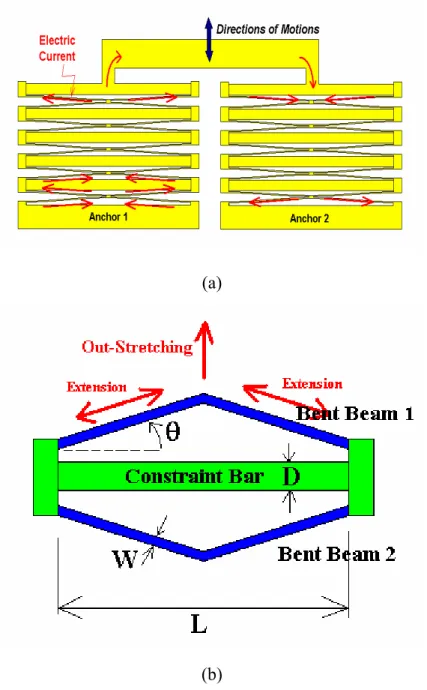
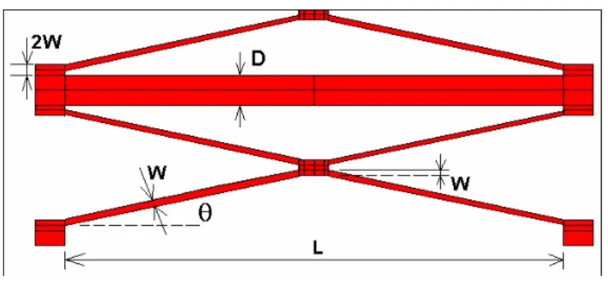
(18) Chapter 2 Design and Analysis. In the following paragraph, the concept design of the three-dimensional LSMD is proposed.. Then, assembly design is also discussed. Simulation comparison of the. three-dimensional and planar LSMD will be discussed finally.. 2.1 Operation Principle of LSMD The structure design of the electro-thermally driven large-stretch micro drive (LSMD) is illustrated in Figure 2-1 (a), which consists of two cascaded compliant structures in parallel. Each cascaded structure is formed by connecting several basic actuation units in series.. Each basic actuation unit is composed of two actuation. beams and one constrainer, as shown in Figure 2-1 (b). In operation, when an electrical potential is applied between Anchor 1 and Anchor 2 to form a close loop as shown in Figure 2-1 (a), a current passes through the actuation beams, and then joule heating causes them to deform.. The actuation beams thermally. expand and lead the actuation unit to stretch outward. Therefore, the output displacement and force are generated from the summation of all basic actuation units in each cascaded structure. Since two cascaded structures are in parallel arrangement, the total output force can be doubled. Thus, more basic actuation units in cascaded structures can effectively magnify the output displacements and forces of the micro drive in compact size. V-shaped bent beams are used here. What’s more, the actuation beam width (W), beam span (L), constrain bar width (D) and the bent angle (θ) between the actuation 8.
(19) beam and constrain bar are varied. The device performance between different geometries would be analyzed.. The parameter definitions are illustrated in Figure 2-2.. (a). (b) Figure 2-1 Design of the long-stretch micro drive (LSMD): (a) two cascaded compliant structures in parallel arrangement; (b) schematic diagram of the basic actuation unit in out-stretching displacement. 9.
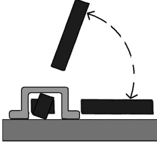
(20) Figure 2-2 The basic actuation unit with V-shaped actuation beam and its parameter definitions. 2.2 Concept Design of the Three-dimensional Long-Stretch Micro Drive In the proposed actuator, the hinge and the LSMD are integrated as shown in Figure 2-3.. The LSMD instead of the original plane will be lifted in the third. dimension. Electric connection is the most important issue in the thesis.. By. metal-based surface micro machining, current could pass from the pad to the LSMD through the metal hinge mechanism. How to fix the LSMD in the third dimension will also be discussed below. The freedom of the LSMD is limited by the geometry of the pin and the staple.. If. the pin is wider than the sum of the pin thickness and the sacrificial copper layers, the LSMD will be unable to rotate a full 90 degrees as Figure 2-4 shown.. Thus, when the. LSMD is lifted, hinge pin will contact the staple directly to form an electric connection. Therefore, current could pass through staple to the hinge and the position of the LSMD will be fixed. Another way to fix the LSMD on the staple is to let the LSMD rotate a full 180 degrees off the substrate as shown in Figure 2-5 and to let the pin and the staple adhere together.. To achieve this aim, the width of the pin must be smaller than the sum of the. thicknesses of the sacrificial copper layers and the pin. Then the welding material is 10.
(21) used to assembly the pin and the staple by welding.. After assembly, hinge pin will. contact the staple indirectly to form an electric connection, too.. Assembly will be. canvassed in the section 2.3. As a DC voltage applied to the pad, the current will be transferred from the staple to the hinge pin (If there is an adhesion layer, current will pass through it, too). In other words, the part of the pin and the staple replace the pad in the planar LSMD.. Figure 2-3 sketch view of the three-dimensional actuator design. Figure 2-4 the LSMD will be unable to rotate a full 90 degrees 11.
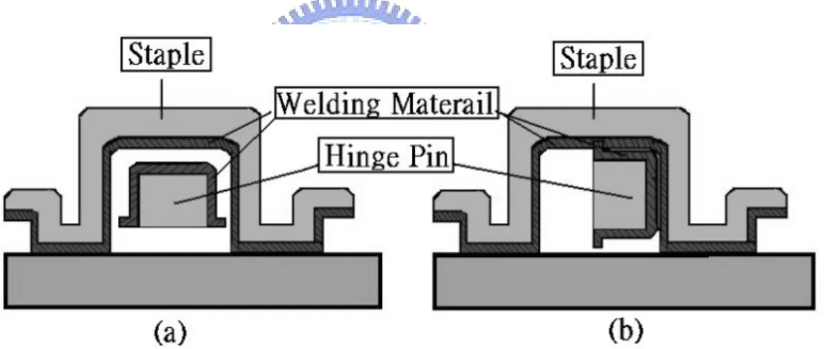
(22) Figure 2-5 the LSMD rotate a full 180 degrees. 2.3 Thermal Assembly Design Without a locking mechanism, welding is used to fix the position of the LSMD. For thermal assembly, the welding material and the heating sources for the melting the welding material are the necessary conditions. In 1991, Howe took the polysilicon which has high resistivity as the heating source, and aluminum is the welding material. In our thermal assembly, metal is taken as the heating source, and tin is the welding material. The main difference between Howe and ours is the position of the welding material. In our thermal assembly, the welding material is not on the circuit. It is just near the heating source. On the contrary, Howe took the welding material as the joint in the circuit. The advantage of our welding is that welding material is not required to be connected to the heating source originally. So that it may be more suitable for suspend structure. The chart and the other difference are shown in Table 2-1. z. Staple Design Figure 2-6 shows sketch of the shape design of the staple which is treated as the. heat source. In Figure 2-6, an electrical current will be applied between area A and area C. At area B, the resistance is larger due to its small cross section when whole staple has uniform thickness. According to the equation of the power, P=I2*R, the power is proportion to the resistance. In other words, power has maximum value at area B. Therefore, when we applied the current on the staple, the temperature of area B which is 12.
(23) the heating region will be higher than other areas due to higher power. The welding material also should be made on the area which will contact the area B of the staple. Figure 2-7 is the cross section view of the staple and the hinge pin with welding materials. As Figure 2-7 (a) shown, the slash areas are the welding materials and both of them could be made under the staple and on the hinge pin. In the heating process, welding materials will be melted at the same time, and both of them will be integrated together after welding as Figure 2-7 (b) shown. z. Operating Temperature According to the experiment in the past, nickel will be oxidized when the. temperature is up to 400℃ in the air. To avoid the oxidation of the nickel LSMD, welding temperature of the hinge pin must be lower than 400℃, or even lower. Therefore, melting temperature of the welding material must be the first consideration and the selection of the welding material will be discussed in the next paragraph. z. Selection of the Welding Material Metals, like Tin and Indium, are the materials of low melting temperature down to. 231.9℃ and 156.6℃ respectively. Vapour of Indium is noxious and will oxidize at high temperature easily, so Tin is a more suitable choice than the indium. Aluminum is also used as an adhesion material.. Aluminum has the properties of high thermal. conductivity and the low melting temperature. Although the melting temperature of the Aluminum is higher than Tin, it is far lower than nickel. Therefore, it is on the list of the consideration, too.. Table 2-2 shows some referenced properties of the nickel,. Tin and aluminum.. 13.
(24) Figure 2-6 Sketch of the thermal assembly design. Figure 2-7 the cross section view of the staple and the hinge before (a) and after (b) welding.. 14.
(25) Table 2-1 Welding Comparison Howe. Ours. Heating Source Polysilicon Material Welding Material Aluminum(660℃). Metal(Nickel or Tin) Tin(232℃). Welding material is on the Welding material isn’t on the circuit circuit. Contact Form. Applied Power. AC. DC z. Features. z z. Welding quality is better. No contact problem.. z. Melting point of welding materials is lower. It may be more suitable for suspend structure.. Table 2-2 Referenced properties of the Nickel, Tin and Aluminum Nickel. Tin. Aluminum. Melting temperature (℃). 1453. 232. 660. Resistivity (nΩ-m). 6.9. 12.6. 2.67. Thermal conductivity (W/mK). 90.5. 66.8. 237. 2.4 Analysis To investigate the thermal mechanical behaviors of three-dimensional LSMD, finite element simulations are conducted by using commercial software ANSYS 6.0. Simulation process includes two steps.. First is nonlinear electro-thermal analysis with 15.
(26) 3-D Solid69 element and followed by nonlinear thermal stress analysis with 3-D Solid45 element.. These two steps include preprocessor and post-processor.. The. details of the analysis setup and the results will be discussed below.. 2.4.1 Analysis Setup The device is made of nickel and fully surrounded with air. A silicon oxide layer is built between the contact pad on top and the single-crystalline silicon substrate on bottom.. Thermal conduction, convection, and nonlinear structural analysis are. considered in the simulations.. Therefore, the temperature distributions of the bent. actuation beams are not uniform in the analysis. The effects of thermal radiations are not considered here due to the low operating temperatures of the LSMD (below 400°C). To run the model efficiently, half-symmetry model of the three-dimensional LSMD with five basic actuation units is shown in Figure 2-8, and material properties used in simulation are listed in Table 2-3. In the preprocessor, a three-dimensional model must be constructed in the first. Then material properties are defined and loaded into the analysis model. Followed is the volume meshing. In the post-processor of the electric-thermal analysis, there are some boundary conditions must be set, such as room temperature setting and the convection coefficient. The bottom faces of the contact pads are set with room temperature to define thermal boundary conditions. Convection loads are applied to all surfaces of the model with constant convection coefficient value of 120. The convection coefficient value will be discussed below.. Initial conditions such as electrical potential are applied to pads.. Then the simulation is solved. After the electric-thermal analysis, we get the result of the distribution of temperature that will be the initial condition of the next analysis step. In addition to 16.
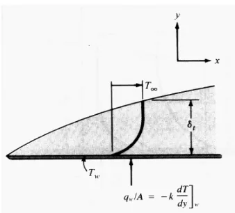
(27) the distribution of temperature, the bottom faces of the contact pads are fixed in nonlinear and large-deflection structural analyses.. After the simulation is solved, we. could get the displacement and stress distribution of the structure finally. 2.4.1.1 Derivation of the thermal convection coefficient In the analysis, heat transfer has great influence on the performance of the three-dimensional LSMD.. As for heat transfer, thermal convection is the most. important factor in this case.. Therefore, thermal convection coefficient will be. calculated below. We assume the device is the uniform temperature plane and consider the system shown in Figure 2-9. The temperature of the plane is Tw , the temperature of the fluid outside the thermal boundary layer is T∞ , and the thickness of the thermal boundary layer is designated as δ t .. At the plate, the velocity is zero, and the heat transfer into. the fluid takes place by conduction, thus the local heat fluxes per unit area, q" , is q" = − k (∂T / ∂y )wall. (2-1). Newton’s law of cooling is shown below, q" = h(Tw − T∞ ). (2-2). The quantity h is called the convection heat-transfer coefficient. Combining these equations, we have h=. − k (∂T / ∂y )wall 3 k = Tw − T∞ 2 δt. (2-3). So that we need only find the temperature gradient at the plane in order to evaluate the heat-transfer coefficient. This means that we must obtain an expression for the temperature distribution.. To do this, an approach similar to that used in the. momentum analysis of the boundary layer is followed. T = Tw. at y = 0. (2-4-a) 17.
(28) ∂T =0 ∂y. at y = δ t. (2-4-b). T = T∞. at y = δ t. (2-4-c). Due to the viscous heating, the velocities must be zero at the plane ∂ 2T =0 ∂y 2. at y = 0. (2-4-d). Equations (2-4-a) to (2-4-d) may be fitted to a cubic polynomial as in the case of the temperature profile, so that T − Tw θ 3 y 1⎡ y⎤ = − = θ ∞ T∞ − Tw 2 δ t 2 ⎢⎣ δ t ⎥⎦. 3. (2-5). The velocity profile which we can choose to satisfy the situation is a polynomial as shown below. 3 y 1 ⎡ y⎤ u = − u∞ 2 δ 2 ⎢⎣ δ ⎥⎦. 3. (2-6). This is the integral energy equation of the boundary layer for constant properties and constant free-stream temperature T∞ 2 d ⎡ H ∂T µ ⎡ H ⎛ du ⎞ ⎤ ⎤ (T∞ − T )udy ⎥ + ⎢ ∫ ⎜⎜ ⎟⎟ dy ⎥ = α ∫ ⎢ 0 0 ⎦ ρC p ⎢ ⎝ dy ⎠ dx ⎣ ∂y ⎥⎦ ⎣. ]wall. (2-7). Inserting the equation (2-5) and the equation (2-6) into the equation (2-7), we can get the below equation when the plate is heated over the entire length.. ζ =. 1 δt −1 / 3 = Pr δ 1.026. where Pr =. (2-8). v. (2-9). α. Inserting the equation (2-8) into the equation (2-3), ⇒h=. 3k 1/ 3 1.026 Pr 2δ. (2-10). The δ would be written in terms of the Reynolds number as 18.
(29) δ x. =. 4.64 Re1 / 2. (2-11). And inserting the equation (2-11) into the equation (2-10) 3 k Re1 / 2 1/ 3 1.026 Pr ⇒h= 2 x 4.64. (2-12). The average heat-transfer coefficient may be obtained by integrating over the length of the plate: L. ∫ hdx = 2h h= ∫ dx 0. (2-13). L. 0. When there is an appreciable variation between wall and free-stream conditions, it is recommended that the properties be evaluated at the so-called film temperature T f , defined as the arithmetic mean between the wall and free-stream temperature,. Tf =. Tw + T∞ 2. (2-14). 2.4.1.2 Calculation of the thermal convection coefficient We assume the temperature of the entire device is 400℃ as the wall temperature, and the room temperature is 25℃ as the free-stream temperature. Tf =. Tw + T∞ 400 + 25 = = 212.5 ℃=490°K 2 2. From Appendix A [J. P. Holman], the properties in the 490°K are Pr = 0.68. v = 37.9m 2 / s × 10 −6 k = 0.04038W / m°C. The length of the device is. x = 1000µm = 1× 10 3 × 10 −6 m = 1× 10 −3 19.
(30) And the velocity of the free-stream u ∞ = 1m / s at 27℃ 1atm Therefore,. Re =. u ∞ × x 1m / s × 1 × 10 3 × 10 −6 m = = 26.385 v 37.9m 2 / s × 10 −6. 3 k Re1 / 2 1/ 3 1.026 Pr h= 2 x 4.64 1/ 2 3 × 0.04038 × (26.385) × 1.026 1/ 3 = × (0.68) 3 −6 2 × 1 × 10 × 10 × 4.64 = 60.497W / m 2 °C The average value of the heat-transfer coefficient is twice this value. h = 2h = 120.994W / m 2 °C. Figure 2-8 Finite element model in half-symmetry used in simulations. 20.
(31) Figure 2-9 Temperature profile in the thermal boundary.. Table 2-3 Material properties used in finite element simulation. Nickel. SC-Silicon. Silicon-Dioxide Dry-Air. 115 [25]. 162. 57. E : Modulus of *. Elasticity (GPa) Temperature D:. Density. dependent: 9040. 2420. 2660 1.293-0.456(273K. (Kg/m³). -773K) Coefficient. of Temperature. thermal. dependent:. Temperature dependent: 0.4. *. Expansion. 12.7-16.8(300K 2.56-4.10(300K. (10 −6 /K). ~800K). ~800K). 0.31. 0.28. 0.245. *. Temperature. 1.1. Temperature. ν. :. Poisson. Ratio κ. :. Thermal 90.5. 21.
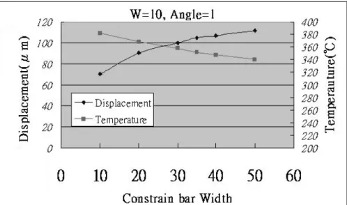
(32) Conductivity. dependent:. dependent:. (W/mK). 146.4-41.8(300. 0.024-0.056(273K. K~800K). ~773K) Temperature. c : Specific Heat. dependent: 443.08. 706.4. 176. (J/Kg-K). 1006-1093(273K~ 773K). ρ : Resisvitity. 13.5. *. *. *. (µΩ-cm). 2.4.2 Simulation Results. From simulation, the temperature is not uniformly distributed along the actuation bent beam and the temperature profiles of each actuation beams are different. Figure 2-10 shows the simulated temperature profile of the three-dimensional LSMD at 2 dc volts where the maximum temperature occurs near the middle of the suspended structure and is below 400°C. Figure 2-11 presents the influence of constraining bar width on output displacement and temperature.. Generally, constraining bar provides clamping force on. both ends of the actuation beam.. Therefore, elongation of constraining bar due to. thermal expansion will depress output displacements of actuation beams. It is found that in wider constraining bar can enhance the output displacements. This is due to lower structural elevated temperatures of wider constraining bars.. Although the. displacement will be larger with constrain bar width, increase of the displacement is limited and a wider constraint bar will takes up more space. Figure 2-12 shows the simulated output displacements and temperature with 22.
(33) various bent beam widths of three-dimensional LSMD at constant applied voltage. The optimal bent beam width around 6 µm is found at the constant applied voltage mode.. For narrower beam widths, the electrical resistances of three-dimensional. LSMD will be higher. Therefore it will consume less electrical power and depress output displacements.. On the contrary, for wider actuation bent beam, electrical. resistances of three-dimensional LSMD become smaller and get more electrical power, however the mechanical stiffness EI of the bent beams may increase too rapidly and depress output displacements.. Figure 2-10 the simulated temperature profile of LSMD in top view. 23.
(34) Figure 2-11 Out-stretching displacements of three-dimensional LSMD with various constrain bar widths under constant applied voltage (2 volts). Figure 2-12 Out-stretching displacements of three-dimensional LSMD (D=35 µm, θ=1°) under various bent beam widths at constant applied voltage (2 volts).. 2.4.3 Results Comparison with Planar LSMD. The models of the planar LSMD and the three-dimensional LSMD are constructed in the same way, and their boundary and initial conditions are also the same. The difference of the simulation between the planar LSMD and the three-dimensional 24.
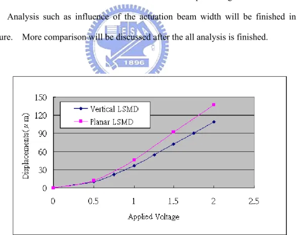
(35) LSMD will be discussed below. Figure 2-13 shows the simulated load-deflection curve and maximum temperature of the planar LSMD and three-dimensional LSMD at various input voltages. It is found that for a three-dimensional LSMD, without the heat conduction through the air gap to the substrate, the temperature of whole LSMD becomes higher.. And the. temperature difference between the actuation beam and constrain bar becomes smaller. Elongation of constraint-bar due to thermal expansion will depress output displacements of actuation bent beams. Therefore, when the temperature of constrain bar is larger, the influence of the depressing output displacement will be lager, too. In other words, the output displacement of three-dimensional LSMD will be smaller than planar LSMD with substrate beneath for heat conduction at the same input voltage. Analysis such as influence of the actuation beam width will be finished in the future.. More comparison will be discussed after the all analysis is finished.. (a). 25.
(36) (b) Figure 2-11 Simulated (a) out-stretching displacements and (b) maximum elevated temperatures of planar LSMD and three-dimensional LSMD at various operating voltages (W=8µm, D=35 µm, θ=1°). 26.
(37) Chapter 3 Fabrication. During this fabrication process of the three-dimensional actuator, the metal-based surface micro machining is developed including lithography, sputtering and electroplating techniques. Besides, electroplating including copper electroplating and nickel electroplating is the main fabricating technique. In this chapter, the electroplating will be discussed. Moreover, the fabricating steps of the device and the assembly process will be shown. At last, fabrication results will be discussed.. 3.1 Copper and Nickel Electroplating The metal-based surface micromachining is used in the fabrication process. To construct the metal device, electroplating is taken as the main technique of the metal-based surface micromachining. Thus whole device including the sacrificial layer and the structure layer will be made of metal. The sacrificial layer and the structure layer are made of copper and nickel, respectively. The equipments and principles of copper and nickel electroplating are similar. So copper and nickel electroplating will be discussed in the same section. During the electroplating process, adhesion and seed layers have to be deposited on substrate as the base before electroplating.. Therefore,. metal selection for the adhesion and seed layers will be discussed firstly. Followed are electroplating equipments setup and the other related items like current density which is most important for the electroplating quality.. 27.
(38) 3.1.1 Selection of the Adhesion Layer and the Seed Layer. Before electroplating, the adhesion layer between the substrate and the seed layer is necessary. In the electroplating, current could be transferred from the cathode to electroplating bath through the seed layer. It shows that seed layer is also essential. The seed layer is better to be thinner and smoother. Therefore the adhesion layer and the seed layer must be selected properly to conduct smoothly and avoid seed layer being stripped from the substrate. Table 3-1 shows testing results of the combination of these two layers. Copper is chosen as the seed layer because of its low electric resistance in the first. Due to the low electric resistance, the seed layer could be very thin for electrical conducting.. Besides, electroplated copper is taken as the sacrificial layer in the. fabrication process and it will be removed in the last releasing process. Therefore, seed layer and the sacrificial layer could be removed simultaneously if their materials are the same. From the testing results, titanium and nickel adhere well as the adhesion layer between the copper and substrate. However, titanium is more suitable than nickel because the device is also made of nickel. The adhesion layer must be removed in the last releasing process. If the device and the adhesion layer are the same materials, the device will be attacked when etching the adhesion layer. Therefore, Ti is adopted as the adhesion layer during the electroplating process.. 28.
(39) Table 3-1 Testing results of the adhesion layer and the seed layer Adhesion Seed Layer. Testing Results. Layer Success. The electroplated copper wasn’t (1). Titanium. Copper. stripped and the Ti layer is removed by BOE without damaging of the nickel structure. Failure. Although the electroplated nickel wasn’t stripped, the electroplated nickel was. (2). Nickel. Copper damaged in the adhesion layer removing process. Failure.. (3). Chromium. The. electroplated. copper. was. Copper stripped from the Cr layer. 3.1.2 Electroplating Bath. In the copper or the nickel electroplating, lots of electroplating baths are available to choose. For copper electroplating, baths are divided into acidic and alkaline bath. Acidic bath is often taken as the device plating and the alkaline bath is taken as the protecting layer. For this reason, copper sulphate bath, a kind of the acidity bath, is chosen as the copper-electroplating bath. Table 3-2 lists the composition of copper electroplating bath. As for nickel electroplating, Watts bath is the most widely used in nickel electroplating due to its fast electroplating velocity and better quality. To quickly make thicker nickel layer, Watts bath is suitable. Table 3-3 lists the composition of nickel electroplating bath.. 29.
(40) Table 3-2. The composition of Copper plating bath Composition. Quantity. CuSO4. 200 g/L. H2SO4. 70 g/L. Cl-. 100 mg/L. CU-352 Bath Burnish Agent. 3.2 ml/L. CU-352 Carrier Burnish Agent. 3.2 ml/L. CU-353 Burnish Agent. 0.8 ml/L. Table 3-3. The composition of nickel plating bath Composition. Quantity. Nickel Sulfamate, Ni(SO3NH2)・4H2O. 400 g/L. Nickel Chloride, NiCl2・6H2O. 5 g/L. Boric Acid, H3BO3. 40 g/L. EPC-30. 10 ml/L. NPA. 2 ml/L. Wetting Agent. 5 ml/L. 3.1.3 Electroplating Equipments. Figure 3-1 shows the pictures of electroplating system used here including copper and nickel electroplating. The system contain the wafer holder, the bath tank, the filter system, the thermostat (only for nickel electroplating system), DC power supply, and control system. The wafer holder is put into the tank. Besides, a conducting wire attached to wafer holder is connected to the DC power supply. The bath tank stores 30.
(41) electroplating the bath, and the bath circulates among the tank, the filter system and the thermostat. The nickel electroplating’s bath temperature is different from the copper electroplating. Nickel electroplating bath must be proceeding at 50℃ to keep the electroplating quality. Therefore, thermostat must be added in the nickel electroplating system which is shown in Figure 3-1 (b). The control system contains the switches of the filter system, the thermostat and the main electrical switch.. (a). 31.
(42) (b) Figure 3-1. Pictures of the system (a) and (b) for copper and nickel electroplating respectively. 3.1.4 Current Density. In electroplating, the structure stress and the smoothness of the electroplated structures are decided by current density. In this electroplating process, current density ranges from 6mA/cm2 to 8mA/cm2.. If the current density is too low, the impurities. will be on the wafer at the same time. structure becomes rough and rugged.. Therefore, the surface of the electroplated. On the contrary, if the current density is too high,. more stresses would be produced and the structures might be deformed. Under the current density of 8mA/cm2, the electroplating speed is about 0.22µm /minutes and 0.18µm /minutes for copper and nickel respectively.. 3.2 Fabrication Process In this fabrication process, the substrate is first deposited with a conductive seed layer. And the following steps will circulate repeatedly. The photoresist is coated and 32.
(43) patterned on the seed layer to act as the plating mold.. Followed, the metal layer is. electroplated in the plating mold to form the metal structure. After the electroplating finished, the resist mold is removed.. At final releasing process, the seed layer and the. sacrificial layer are removed to obtain the suspended metal structure. In this section, process flow of the whole device will be shown in section 3.2.1, and welding test process will be particular discussed in section 3.2.2.. 3.2.1 Fabrication Process flow. Fabrication Process (A) without the welding material is shown in Figure 3-2. And Figure3-3 shows the fabrication Process (B) with the welding material which is discussed in the section 2.3. The mask#1, mask#2, and mask#3-1 and mask#4 are the same in fabrication processes (A) and (B). The Process (B) has more than one mask, mask#3-2 at step c). The Detailed fabrication steps are explained in the Table 3-4. The photoresist used in the lithography is positive photoresist AZP4620® (AZ 4000 series, Clariant). After releasing process, there are two assembly ways to lift up and fix the LSMD in the immovable position.. One is the directly contact by matching the size, and it will. be lifted up vertically by probe without toppling down such as fabrication Process (A). The other is utilizing the adhesion layer to fix the LSMD such as fabrication Process (B). After releasing process, wafer will be reversed and the LSMD can be hanged vertically by gravity force. However, when wafer is reversed, it is difficult to apply the voltage to the pads by probe. To overcome the problem of the electrical conduction, wire bonding is used. By wire bonding, electrical potential can be applied from the wire to the pads without using the probe. Therefore, before reversing the wafer, wire bonding must be done for Process (B) in the first.. 33.
(44) Table 3-4 Fabrication steps of the three-dimensional actuator Process A. Process B. Step a) A 5000Å oxide layer utilizing wet oxidation is deposited on the wafers as the electrical isolation layer. Then a 300Å Ti adhesion layer and a 1500 Å copper seed layer are deposited by sputter on whole wafer. Followed, 5µm photoresist is spun, exposed and developed (mask#1). After that, the 5 µm copper is electroplated to act as the first sacrificial layer. Step b) A 27µm photoresist is spun, exposed and developed (mask#2). Then the 11µm thick nickel layer electroplating is performed to form the LSMD and hinge pin. Step c) A 27µm exposed (mask#3-1).. photoresist and. is. spun, A 27µm photoresist is spun, exposed. developed and. developed. (mask#3-1).. Then the 5 µm Followed is the welding material,. copper layer is electroplated as the Tin, deposited by sputter. second sacrificial layer. After PR removing, a 27µm photoresist is spun, exposed and developed (mask#3-2), again. Then the. 10. µm. copper. layer. is. electroplated as the second sacrificial layer. Then the welding material, tin, is deposited by sputter. Step d) A 27µm photoresist is spun, exposed and developed (mask#4). Then the 20µm thick nickel film is electroplated.. 34.
(45) Step e) Releasing the sacrificial layer utilizing liquid ammonia with hydrogen peroxide (18 minutes), and Ti layer is removed by BOE. Then, by a rinse in deionized (DI) water to remove the solution. Followed is air drying. Step f) LSMD is lifted up by the probe. In the first, wire bonding is used to conduct the pad to the wire. Then wafer will be reversed and the LSMD can be hanged vertically by gravity force. Followed is applying the voltage to the pads near the adhesion layer to fix the LSMD.. 35.
(46) Figure 3-2 Fabrication Process (A). 36.
(47) Figure 3-3 Fabrication Process (B) with welding materials. 37.
(48) 3.2.2 Welding Test Process. The aim of the welding test process is to verify the possibility of the welding. A tin line will be put on the staple as the Figure 3-4 shown. In this test process, we hope that the tin line will be melted and connected with the staple. The Process (C) flow for welding test is shown in Figure 3-5. First, a 5000Å oxide layer utilizing wet oxidation is deposited on the wafers as the electrical isolation layer. Then a 300Å Ti adhesion layer and a 1500 Å copper seed layer are deposited by sputter on whole wafer. Followed, 5µm photoresist is spun, exposed and developed (Mask#1) as shown in step (a). After that, the 5 µm nickel is electroplated as the pad layer in step (b). Followed, the 0.25µm tin is sputtered in step (c). Without removing the PR, the 27µm PR is spun on the tin layer, exposed and developed (Mask#2) in step (d). Then the 15µm thick nickel film is electroplated as the staple in step (e). Followed, the 2µm tin is sputtered in step (f). Finally, the PR is removed by acetone and the adhesion layer is etched by etchants.. Figure 3-4 the tin line on the staple. 38.
(49) Figure 3-5 Fabrication Process (C) for welding test.. 3.2.3 Fabrication parameter. Table 3-5 lists details of photoresist process used in the fabrication including 5µm and 27µm thick. Table 3-6 lists current density of every step in the electroplating fabrication process including nickel and copper. Table 3-5. Process of AZP4620 in UV depth lithography Operation Spin Coating. Description~5µm. Description~27µm. (1) 1300rpm×20sec. 850rpm×35sec. (2) 3100rpm×40sec.. Relaxation. 5 min.. 5 min.. Soft bake. 5min., 90°C. 20min., 90°C. Relaxation. 5 min. 60 min.. Edge Beam Removal. No. By Acetone. Exposure. 7sec. (46mW/cm²). 27sec. (46mW/cm²). Development. 1 min. in FHD-5. 3 min. in FHD-5 39.
(50) Table 3-6. Current density and Electroplating Velocity. Current Density. Electroplating Velocity. (mA/㎝ 2). (um/10mins). (A),(B)/Mask#1. 4.222. 1.67. Copper. (A),(B)/Mask#1. 8.317. 1.25. Nickel. (A),(B)/Mask#3. 8. 2.25. Copper. (A),(B)/Mask#4-1 7.4. 1.67. Nickel. (B)/Mask#4-2. 6.992. 1.41. Nickel. (C)/Mask#1. 8. 2.25. Nickel. (C)/Mask#2. 8. 2.25. Nickel. Process/Mask. Nickel/Copper. 3.3 Fabrication Results In this fabrication, not all of the processes were successful. The results of Process (A), Process (B) and Process (C) will be shown and discussed respectively. z. Process (A). Process (A) was made successfully including the structure fabrication and the releasing step. No welding material was used in fabrication Process (A), so it was lifted by probe as shown in Figure 3-6 (a). Figure 3-6 (b) shows close view of the actuation beam. The dimension of lifted LSMD shown in Figure 3-6 (a) before actuation is 2000 µm wide, 500 µm high, and 13 µm thick with 10 µm actuation bent beam width. The released hinge structure for the Process (A) is shown in Figure 3-7. In Figure 3-7, pin of the LSMD and staple contact each other directly. And the thickness of the staple is 10 µm in Figure 3-7. z. Process (B). Process (B) was not finished at the last releasing step, so the three dimensional 40.
(51) LSMD made in Process (B) was not lifted and tested. However, the whole structure was made successfully. The released hinge structure for the Process (B) is shown in Figure 3-8. Figure 3-8 shows the welding materials on staple before and after removing titanium which was etched by B.O.E. in the releasing process. Before removing titanium, the tin strip has separated from the pin. Besides, it shows that the adhesion between the tin and the nickel is not very good after releasing copper. After removing titanium, tin film was also removed simultaneously. It may due to bad quality of tin film. In Figure 3-8, the tin strip was survived but another tin film under the staple was gone. In the fabrication process, the tin film was sputtered, followed is the nickel electroplating. Lithography process must be done first before electroplating, so that the tin film will be exposed under the atmosphere and tin film was oxidized. Thus, the surface of the tin film was very rough and the adhesion between staple and nickel became worse. Therefore, all were immersed in BOE, the oxidized tin film was etched, and the tin film was also striped in BOE. z. Process (C). The released hinge structure for the Process (C) is shown in Figure 3-9. The thickness of the staple which was made of nickel is 15 µm as shown in Figure 3-9 (c).. 41.
(52) (a). (b) Figure 3-6 Fabrication result. (a) The lifted LSMD; (b) Close view of the actuation beam. 42.
(53) Figure 3-7 Fabrication result of the staple for Process (A). Figure 3-8 Fabrication result of the staple for Process (B). Figure 3-9 Fabrication result of the staple for Process (C). 43.
(54) Chapter 4 Testing. Now, some devices have been fabricated and LSMD have been lifted up by probe successfully. To demonstrate the feasibility of the electrical connection, the performance of the three-dimensional actuator will be shown in this chapter. Moreover, to prove the welding possibility, the welding test results will also be shown below. In this chapter, experimental setup will be illustrated in the first, and the measure results will be shown below. Finally, the welding test results will be shown at last.. 4.1 Experimental Setup In last releasing process, the LSMD was lifted up, and the hinge ruler, as Figure 4-1 shown, was lifted at the same lifted angle. So the displacement of the LSMD and the ruler could be observed on the same plane by the microscope. Followed, a wire and the LSMD pad were soldered together and the die was set on a holder as shown in Figure 4-2. The holder is tied perpendicular to the station for observing conveniently when measuring the displacement as shown in Figure 4-3. Whole measuring system including microscope, station, the CCD camera, computer with image capture and power supplier is shown in the Figure 4-4.. 44.
(55) Figure 4-1 the whole view of the LSMD and ruler; the enlarged view of the ruler. The distance of ruler unit is about 20 µm.. Figure 4-2 the die attached on the holder. 45.
(56) Figure 4-3 the holder tied perpendicular to the station. Figure 4-4 Schematic drawing of the measurement system. 4.2 Measurement results The fabrication Process (A) was made successfully, and fabricated LSMD was taken as the measurement sample in the output displacement measurement. The calibrated output displacements of three-dimensional LSMD are shown in Fig. 4-5 and out-stretching displacements can reach 84 µm at input voltage of 2 V. Figure 4-6 demonstrates such three-dimensional LSMD before and after applying a 2 dc voltage. 46.
(57) From these data, the electrical conduction has been proved obviously firstly. And the tendencies of the experimental and the simulation results are the same even though the displacement of the experiment is smaller than the one of the simulation. The difference between them may be due to the contact resistance. The contact areas of the staple and the hinge pin fabricated here are limited, so they are connected partly. In other words, the contact resistance is larger than the simulation model. Therefore, the displacement of the experiment is smaller than one of the simulation.. 120 Displacement. 100 Exp.. 80. FEM. 60 40 20 0 0. 0.5. 1. 1.5. 2. 2.5. Applied Voltage. Figure 4-5 Testing results of the three-dimensional LSMD with geometry parameter of L=1000µm, W=10µm, D=35µm, and θ=1°. 47.
(58) Figure 4-6. Operation close-up view of the fabricated three-dimensional LSMD which delivers stretching displacements up to 84µm at 2 dc volts. The distance of ruler unit is about 20 µm. (W=10 µm, θ=1°, D=35 µm). 4.3 Welding Test Results Although the fabrication Process (B) for welding ailed, some information about the welding from fabrication process (c) test is still useful for welding. Table 4-1and Table 4-2 show applied condition items for different size including applied current, time, the calculated power per micrometer and the calculated calorific capacity per micrometer. , the maximum power which won’t cause the staple broken is shown in the Table 4-1. While the power per micrometer did not exceed 0.1 mW/µm, the staple was heated and the color of the staple became red, but it did not break as Figure 4-7 shown. As long as the maximum power per micrometer was decided, the maximum applied current for different staple size could be calculated. To base on the data of the Table 4-1, the current which won’t exceed the maximum power was taken as applied current as shown in Table 4-2. And Table 4-2 also shows the calorific capacity which needs to melt the tin line. As the calculated calorific capacity per micrometer was up to 2.2 mJ/µm, the tin 48.
(59) line was melted and connected with the staple as shown in Figure 4-8. Table 4-1 Record of the maximum power test. Number. cross-section (µm2). Resistance per µm (Ω). Applied current(A). Power per µm Results (mW/µm). 28-1-L. 2190. 3.123E-05. 1.5. 0.070. Success. 28-5-R. 1730.1. 3.954E-05. 1.6. 0.101. Success. 28-6-L. 1730.1. 3.954E-05. 1.6. 0.101. Success. 28-6-R. 1730.1. 3.954E-05. 1.7. 0.114. Broken. 28-9-L. 3186.45. 2.147E-05. 2.2. 0.104. Success. Table 4-2 Record of the success welding Resistance per Applied Number µm current(A) (Ω). Power per µm (mW/µm). Applied Time (s). Calorific Capacity µm (mJ/µm). 28-4-R. 1.971E-05. 2. 0.050. 28. 2.207. 28-8-R. 2.147E-05. 1.9. 0.077. 30. 2.325. 28-8-L. 2.147E-05. 1.9. 0.077. 32. 2.480. 28-9-R. 2.147E-05. 1.8. 0.070. 35. 2.434. Figure 4-7 the staple. 49. per.
(60) Figure 4-8 the tin line melted. 50.
(61) Chapter 5 Conclusion. 5.1 Summary The design, simulation, fabrication and testing of the three-dimensional large-stretch micro drive (LSMD) are presented in this thesis. By combining mechanical hinge and metal-based surface micromachining techniques, the LSMD is shown to be successfully lifted and actuated. Several parameters, width of actuation beams, width of constraining bar and heat transfer condition are found to have strong influence on the output performances of the LSMD. Fabrication and testing results of LSMDs are shown with output displacement up to 84µm at input voltage of 2volts. The welding test results may be also helpful for the other thermal welding. The fabrication technique presented here may benefit other lifted micro sensors or micro actuators with the need of electrical connection.. 5.2 Future Work In the fabrication process, Process (B) was not finished due to the tin film quality. In the future, we may take the tin electroplating to get better quality and the thicker staple. The staple may be made by electroplating and it is taken the heating source and welding material at the same time. From the welding test, staple design offered enough power to melt the tin. We believed that the tin staple as the heating source and welding material could be melted.. 51.
(62) Reference Akiyama, T.; Collard, D.; Fujita, H., “Scratch drive actuator with mechanical links for self-assembly of three-dimensional MEMS”, Microelectromechanical Systems, Journal, Volume: 6 Issue: 1, Page(s): 10 -17, March 1997 Ebefors, T.; Kalvesten, E.; Vieider, C.; Stemme, G., “New robust small radius joints based on thermal shrinkage of polyimide in V-grooves”, Solid State Sensors and Actuators, 1997. TRANSDUCERS '97., Volume: 1, Page(s): 675 –678, 16-19 June 1997 Fan, L., Wu, M.C., Choquette, K.D., Crawford M.H., “Self-Assembled Microactuated XYZ stages for optical Scanning and Alignment”, Transducers’97, pp.16-19, June 1997. Fedder, G.K.; Howe, R.T., “Thermal assembly of polysilicon microstructures” , Micro Electro Mechanical Systems, 1991, MEMS '91, Proceedings. 'An Investigation of Micro Structures, Sensors, Actuators, Machines and Robots'. IEEE , Page(s): 63 –68, 30 Jan.-2 Feb. 1991 Harmening, M.; Bacher, W.; Bley, P.; El-Kholi, A.; Kalb, H.; Kowanz, B.; Menz, W.; Michel, A.; Mohr, J., “Molding of three dimensional microstructures by the LIGA process”, Micro Electro Mechanical Systems, 1992, MEMS '92, Proceedings. 'An Investigation of Micro Structures, Sensors, Actuators, Machines and Robot'. IEEE., Page(s): 202 –207, 4-7 Feb. 1992 Hsu, C.P, Liao, T.S., and Hsu, W., “Electro-thermally driven long stretch micro drive with monolithic cascaded actuation units in compact arrangement,” Transducers’03, Vol. 1, pp. 348-351, Boston, USA, 2003. Iwase, E.; Shimoyama, I.; Takeuchi, S., “Sequential batch assembly of 3-D microstructures with elastic hinges by a magnetic field”, Micro Electro Mechanical Systems, 2002. The Fifteenth IEEE International Conference, Page(s): 188 –191, 2002 Kaajakari, V.; Lal, A., “Electrostatic batch assembly of surface MEMS using 52.
(63) ultrasonic triboelectricity”, Micro Electro Mechanical Systems, 2001. MEMS 2001. The 14th IEEE International Conference, Page(s): 10 –13, 21-25 Jan 2001 Kiaditis, P.E.; Bright, V.M.; Harsh, K.F.; Lee, Y.C., “Prototype microrobots for micro positioning in a manufacturing process and micro unmanned vehicles”, Micro Electro Mechanical Systems, 1999. MEMS '99. Twelfth IEEE International Conference, Page(s): 570 –575,17-21 Jan. 1999 Koide, A.; Tanaka, S., “Simulation of three-dimensional etch profile of silicon during orientation dependent anisotropic etching”, Micro Electro Mechanical Systems, 1997. MEMS '97, Proceedings, IEEE. Tenth Annual International Workshop, Page(s): 418 –423, 26-30 Jan. 1997 Lai, K.W.C.; Hui, A.P.; Li, W.J., “Non-contact batch micro-assembly by centrifugal force” Micro Electro Mechanical Systems, 2002. The Fifteenth IEEE International Conference, Page(s): 184 –187, 20-24 Jan. 2002 Massoud-Ansari, S.; Mangat, P.S.; Klein, J.; Guckel, H., “A multi-level, LIGA-like process for three dimensional actuators”, Micro Electro Mechanical Systems, 1996, MEMS '96, Proceedings, Page(s): 285 -289, 11-15 Feb. 1996 Nakamura, Y.; Nakamura, S.; Buchaillot, L.; Fujita, H., “A three-dimensional shape memory alloy loop actuator, Micro Electro Mechanical Systems”, MEMS '97, Proceedings, IEEE. Tenth Annual International Workshop, Page(s): 262 –266, 26-30 Jan. 1997 Pister K.S.J., Judy M.W., Burgett S.R.,Ffearing R.S., “Microfabricated hinges”, Sensor and actuators A. 33 pp-249-256, 1992 Reid, J.R., Bright, V.M., Butler, J.T., “Automated assembly of flip-up micromirrors” Sensors and Actuators A, 66, pp. 292-298, 1998. Syms, R.R.A., “Equilibrium of hinged and hingeless structures rotated using surface tension forces”, Microelectromechanical Systems, Journal, Volume: 4 Issue: 4, Page(s): 177 -184, Dec. 1995 Syms, R.R.A.; Gormley, C.; Blackstone, S., “Surface tension powered self-assembly of 3D MOEMS devices using DRIE of bonded silicon-on-insulator wafers”, 53.
(64) Demonstrated Micromachining Technologies for Industry IEE Seminar, 29 March 2000 Yoonsu Choi; Kieun Kim; Allen, M.G.; “Continuously-varying, three-dimensional SU-8 structures: fabrication of inclined magnetic actuators”, Micro Electro Mechanical Systems, 2002. The Fifteenth IEEE International Conference, Page(s): 176 –179, 20-24 Jan. 2002 ,. 54.
(65)
數據

+7

相關文件
Robinson Crusoe is an Englishman from the 1) t_______ of York in the seventeenth century, the youngest son of a merchant of German origin. This trip is financially successful,
fostering independent application of reading strategies Strategy 7: Provide opportunities for students to track, reflect on, and share their learning progress (destination). •
Strategy 3: Offer descriptive feedback during the learning process (enabling strategy). Where the
Wang, Solving pseudomonotone variational inequalities and pseudocon- vex optimization problems using the projection neural network, IEEE Transactions on Neural Networks 17
Hope theory: A member of the positive psychology family. Lopez (Eds.), Handbook of positive
volume suppressed mass: (TeV) 2 /M P ∼ 10 −4 eV → mm range can be experimentally tested for any number of extra dimensions - Light U(1) gauge bosons: no derivative couplings. =>
incapable to extract any quantities from QCD, nor to tackle the most interesting physics, namely, the spontaneously chiral symmetry breaking and the color confinement..
• Formation of massive primordial stars as origin of objects in the early universe. • Supernova explosions might be visible to the most
