國 立 交 通 大 學
材 料 科 學 與 工 程 學 系
博 士 論 文
新穎仿生奈米材料三部曲:
蛾眼結構、壁虎膠帶和玫瑰花瓣表面
A Trilogy of Novel Biomimetic Nanomaterials:
Moth Eye Structures, Gecko Tapes
and Rose Petal Surfaces
研 究 生 : 吳佳典 Chia-Tien Wu
指導教授 : 柯富祥 Fu-Hsiang Ko
新穎仿生奈米材料三部曲:
蛾眼結構、壁虎膠帶和玫瑰花瓣表面
A Trilogy of Novel Biomimetic Nanomaterials:
Moth Eye Structures, Gecko Tapes and Rose Petal Surfaces
研 究 生:吳佳典
Student:Chia-Tien Wu
指導教授:柯富祥 Advisor:Fu-Hsiang Ko
國 立 交 通 大 學
材 料 科 學 與 工 程 學 系
博 士 論 文
A Dissertation Submitted toDepartment of Materials Science and Engineering College of Engineering
National Chiao Tung University in partial Fulfillment of the Requirements
for the Degree of Doctor of Philosophy in Materials Science and Engineering
March 2011
Hsinchu, Taiwan, Republic of China
Acknowledgment
『因為需要感謝的人太多了,就感謝天吧。無論什麼事,不是需要先人的遺 愛與遺產,即是需要眾人的支持與合作,還要等候機會的到來。越是真正做過一 點事,越是感覺自己的貢獻之渺小。』
新穎仿生奈米材料三部曲:
蛾眼結構、壁虎膠帶和玫瑰花瓣表面
研究生:吳佳典 指導教授:柯富祥
國立交通大學材料科學與工程學系
摘 要
仿生科技近年來成為研究材料科學一個熱門的領域。科學家透過模仿大自然 的生物研究出各種具有不同功能的人造材料,其效能甚至遠高於自然本身所具備 的。在本篇論文中,我們提出三種新穎的功能性仿生奈米材料起源於蛾眼結構、 壁虎腳和玫瑰花瓣。 蛾眼是由約300奈米高和間隔的突起物所組成之類最密堆積結構,可以有效 地降低其反射率。因此,我們將金屬沉積在鋁和基板之中,利用陽極氧化的方式 處理,這層金屬也會隨之氧化而形成奈米結構點狀陣列,有如蛾眼結構。並且我 們可操控這些結構,由空心到實心,或由半球形到錐狀的陣列。利用這些次波長 的奈米錐狀陣列,我們可以應用在不同的基本上形成抗反射層對於任何角度的入 射光,並具有良好的機械性質。此外,這種空心的錐狀結構也被我們拿來開發成 新穎的光電極結構並應用在增進染敏太陽能電池的效率。透過自主裝的二氧化鈦 空心錐狀陣列和二氧化鈦奈米管壁並用陽極氧化鋁相互隔開已經被我們沉積在 在導電透明基板上。此種結構應用在染敏電池上可以增加染料接觸面積、提供更 直接的電子傳輸路徑並能降低電子電洞的的復合,因此可提升光電轉化之效率。 由壁虎腳所引起的乾式黏附力已引起了各界的關注,透過表面的粗糙度和指 向性的改變,使其擁有強大的黏附力和微弱的脫附力且可重複使用為其迷人之處。 近來,關於壁虎腳的仿生結構在理論及實驗方面的研究已被相繼提出。然而,這些研究與自然的壁虎相比之下,有著受限於材料方面的缺點;但在我們的研究中, 我們設計了一有效的方法來製作出創新的結構來更符合理想的乾式吸附力。我們 首次提出,以去耦兩階段硬式陽極氧化的方式,來製作出長1.3微米、直徑380 奈米的錐形陽極氧化鋁模板;經過翻模的過程後,得到了具有傾斜角度的錐狀奈 米陣列。此錐狀奈米陣列在大面積的表現上具備了出色的方向性、可重複使用性 及水潔淨的特性。與一般的柱狀奈米陣列相比,錐狀奈米陣列有更好的穩定性和 自潔淨的特性。藉由錐狀奈米陣列在各具方向性的力上亦有出色的表現:剪力可 達到每平方公分8牛頓之強, 而反方向的脫附力卻僅需要每平方公分1.4牛頓。 不同於蓮葉效應,最近幾年科學家被玫瑰花表面所深深吸引,其表面具有超 疏水的特性和高水滴吸附力。此種現象是由花瓣上面微米尺度的凸起和奈米結構 所產生。直至今日,許多研究者仍對如何去製造出此等複雜的結構並使其應用而 感到困擾。我們發展出一種由下而上的方法:藉由簡單的酸雕刻技術來製作具有 高水滴吸附力和自潔淨特性的超疏水聚二甲基矽氧烷(PDMS)。此類花瓣的聚二 甲基矽氧烷其有30微米的寬度、奈米皺褶約在500奈米和小於100奈米的奈米結構。 在長時間的檢測下,其也能展現大於150度的水滴接觸角。更甚者,此類花瓣展 現了高水滴吸附力達到35.8 N/m2。除此之外,從酸雕刻技術得來的兩種超疏水 表面讓我們得以用來製造一個新型無殘留的印章。其超疏水且對水滴具吸附力的 區域可用於將染料從印章轉移至紙上。而超疏水具備自潔淨的區域可以避免染料 沾附上去。
A Trilogy of Novel Biomimetic Nanomaterials:
Moth Eye Structures, Gecko Tapes and Rose Petal Surfaces
Student: Chia-Tien Wu
Advisor: Fu-Hsiang Ko
Department of Materials Science and Engineering
National Chiao Tung University
Abstract
Biomimetics is a freshly explored area of materials science that deals with the science of copying or improving upon that which is found in nature. Scientists commonly produce artificial materials with properties that improved from what occurs naturally. In this thesis, we demonstrate three types of novel functional nanomaterials inspired by moth eyes, gecko feet and rose petals.
Moth eyes consist of quasi-close-packed nipples having heights and spacings typically of less than 300 nm, which reduces reflection from their compound eyes. We found, a metal whose oxide form has a higher ionic conductivity than alumina was used as an underlayer preceding an Al anodization process, the underlying metal would be also oxidized and thereby form metal–oxide nanostructures as Moth-eye structures. We modulate the metal–oxide nanomaterials to form, hollow-to-solid and hemisphere-to-cone nanostructure arrays. We employ subwavelength nanocone arrays as Moth-eyes structures for high-performance antireflection coatings. These oxide nanostructures greatly suppress reflectance over a large range of wavelengths and angles of incidence and display a good mechanical stability. Also, we introduce these
nanocones as a new photoelectrode architecture for improved efficiency of dye-sensitized solar cells (DSSCs).A facile synthesis of self-organized hollow TiO2
nanocones under porous anodic alumina (PAA) featuring TiO2 nanotubes (NTs)
within was grown directly on a fluorine-doped tin oxide (FTO) substrate. The novel structure combines two types of TiO2 materials—0-D nanocones and 1-D NTs—to
benefits from a large contact area, direct electron transport path, and slow recombination of electrons.
A gecko is the largest animal that can produce high dry-adhesion to support its weight with a high factor of safety. The secret of the gecko‘s adhesive properties lies in the hairy microstructure and nanostructure of gecko feet. We designed the efficient method of an innovate structure for ideal dry adhesives. A taper anodic alumina oxide mold with a length of 1.3 μm and a diameter of 380 nm was fabricated using decoupling two-step hard-anodization process which was firstly reported by us. After molding, taper-shaped nanohair array with slanted angle was presented. The approach to fabricate angled taper nanohair arrays obtained an excellent directional, reusable, and water cleanable use in large area. A remarkably directional force exhibited by angled taper nanohair arrays was showing here with strong shear attachment (8 N/cm2) in the gripping direction and easy releasing (1.4 N/cm2) in the reverse direction.
Unlike ―Lotus effect‖, the petal‘s surface which has superhydrophobicity and high water adhesion was fascinated by scientists in recent years. The phenomenon is induced by the microscale convex and nanostructures upon the petal. To mimic the petal‘s surface, we developed a bottom-up method by the simple acid texture technique to fabricate the superhydrophobic PDMS surface with high water adhesion and self-cleaning ability. The resulting petal-like PDMS had convexes about 30 μm in diameter, nanowrinkles around 500 nm in width and nanostructures less than 100 nm. A high water contact angle larger than 150° was displayed. Moreover, the petal-like
PDMS exhibited the high water adhesion up to 35.8 N/m2. In addition, the two superhydrophobic surfaces from the acid texture technique allowed us to fabricate a modern nonresidual stamp. The superhydrophobic and water adhesive area is applicable to transport the dye from the stamp to a paper. The superhydrophobic and self-cleaning region avoids the adhesion of dye.
Contents
Acknowledgment ... i Abstract (Chinese) ... ii Abstract (English) ... iv Contents ... vii List of Tables ... ix List of Figures ... x List of Abbreviations ... xx Chapter 1: Overview ... 1 1.1 Nanotechnology ... 1 1.2 Biomimetic Nanomaterials ... 2 1.3 Thesis Organization ... 3Chapter 2: Design of Hollow–to–Solid Moth–Eye Structures Using Anodic Nanocones for High-Performance Optics and Improved Photovoltaic Cells ... 7
2.1 Introduction ... 7
2.1.1 Nanostructures under Porous Anodic Alumina ... 7
2.1.2 Subwavelength Moth–Eye Structure for Antireflection ... 8
2.1.3 Nanomaterials for Improved Dye–Sensitized Solar Cells ... 10
2.2 Materials and Methods ... 13
2.3 Results and Discussions ... 19
2.3.1 Self-Organized NDAs onto a Substrate ... 19
2.3.2 Antireflection Properties of NCAs on Si ... 22
2.3.3 Design of Artificial Hollow NCA for High-Performance Optics ... 25
2.3.4 TiO2 NTs and Hollow NCAs for the Improved Efficiency of DSSCs ... 32
2.4 Summary ... 40
Chapter 3: An Anisotropic, Highly Stable and Water–Cleanable Gecko Adhesion via Innovative Design of Taper Nanohairs ... 73
3.1 Introduction ... 73
3.1.1 Gecko-Inspired Artificial Structure for Adhesion ... 75
3.1.2 Geometry-Controllable Templates from PAA ... 85
3.2 Materials and Methods ... 89
3.3.1 Fabrication of Desirable Taper PAA Templates ... 91
3.3.2 Design of Ideal Nanohairs for Gecko Adhesion ... 93
3.3.3 Adhesive Properties for Taper Nanohairs ... 97
3.4 Summary ... 101
Chapter 4: Kiss from a Rose: Bioinspired Superhydrophobic and High-Water Adhesive Surfaces for Innovative Imprint Technique ... 124
4.1 Introduction ... 124
4.1.1 Lotus Effect: A Superhydrophobic and Self-Cleaning Surface ... 124
4.1.2 Rose-Petal Effect: A Superhydrophobic and High Adhesive Surface .... 126
4.2 Materials and Methods ... 129
4.3 Results and Discussions ... 131
4.3.1 Superhydrophobic Periodic Wrinkles on Plane PDMS ... 131
4.3.2 High-Water Adhesive Properties of Petal-Like Surfaces ... 135
4.3.3 Innovative Applications of Petal-Like Surfaces ... 138
4.4 Summary ... 139
Chapter 5: Conclusions ... 167
List of Tables
Table 2.1 ... 71 DSSC performance metrics. Table 3.1. ... 103 MA versus HA in 2.5% H3PO4. Table 3.2. ... 103The comparison between different types of polymer-based gecko adhesives (N/A represents ―no information‖).
Table 3.3 ... 105
Measurement of contact angle for various cases with a dry adhesive pad.
Table 4.1 ... 141
The treatment conditions were listed above, in which, S/N presented the volume ratio of sulfuric acid over nitric acid.
Table 4.2 ... 142
Expected absorption band in FT-IR spectra of PDMS and common functional groups.
Table 4.3 ... 143
List of Figures
Figure 2.1. ... 43
The illustrated geometry of the RCWA configuration
Figure 2.2. ... 44
Top-view SEM image of PAA film anodizing in 0.3 M oxalic acid at 40 V after a pore-widening treatment
Figure 2.3. ... 45
A typically chronoamperical curve was recorded during the anodization.
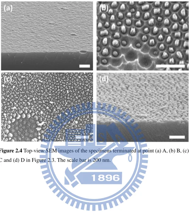
Figure 2.4. ... 46
Top-view SEM images of the specimens terminated at point (a) A, (b) B, (c) C and (d) D in Figure 2.3. The scale bar is 200 nm.
Figure 2.5 ... 47
(a) Cross-sectional SEM image of the nanodots embedded in porous alumina film. (b) Slide-view SEM image of nanodot arrays after removing alumina film. The scale bars are 100 nm.
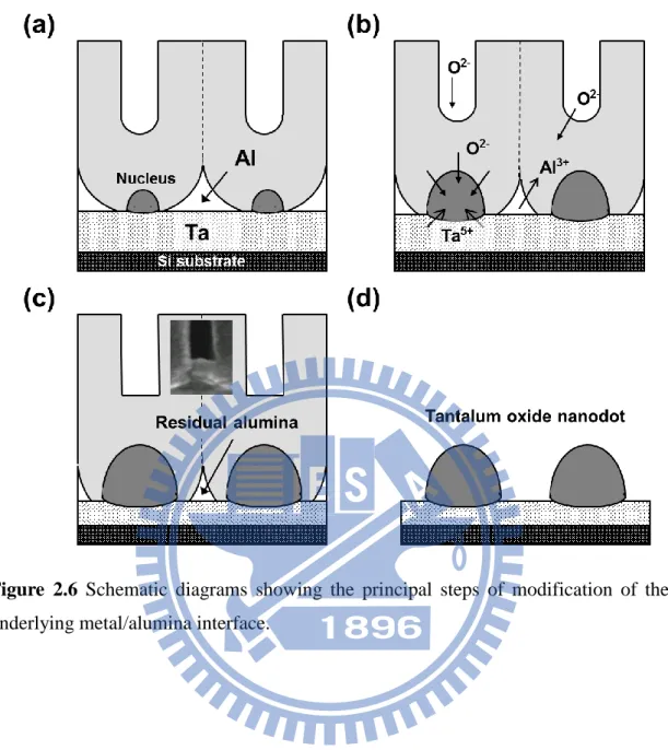
Figure 2.6. ... 48
Schematic diagrams showing the principal steps of modification of the underlying metal/alumina interface.
Figure 2.7 ... 49
XPS depth-profile analysis of Ta 4f spectrum for tantalum oxide nanodots on Si substrates at normal incidence. The bombardment of Ar+ sputtering was used to examine the inner composition; each sputter cycle lasted 5 min.
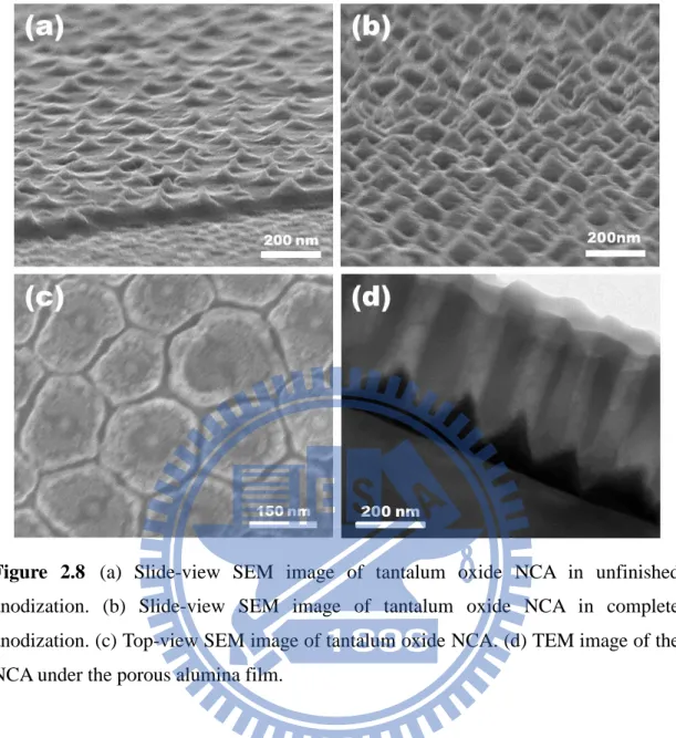
Figure 2.8 ... 50
(a) Slide-view SEM image of tantalum oxide NCA in unfinished anodization. (b) Slide-view SEM image of tantalum oxide NCA in complete anodization. (c) Top-view SEM image of tantalum oxide NCA. (d) TEM image of the NCA under the porous alumina film.
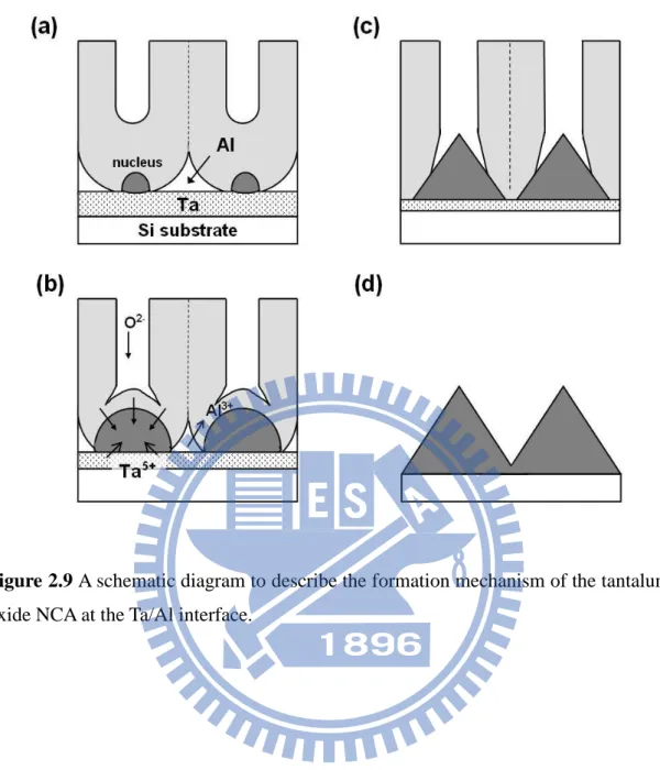
Figure 2.9 ... 51
at the Ta/Al interface.
Figure 2.10 ... 52
XPS depth-profile analysis of Ta 4f spectrum for tantalum oxide NCA on Si substrates at normal incidence. The Ar+ sputtering of 5 and 30 min was used to examine the inner composition.
Figure 2.11 ... 53
The spectroscopic measurements of broadband reflectance for the blank silicon wafer, the anodic tantalum oxide film and tantalum oxide NCA, respectively.
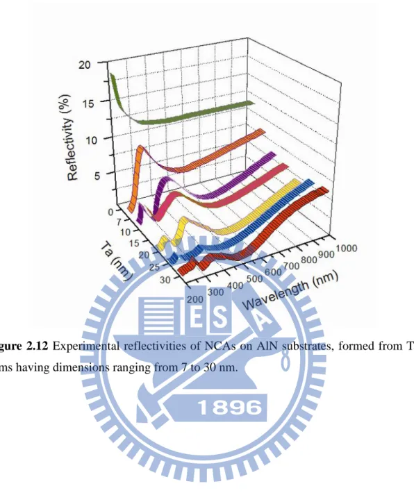
Figure 2.12 ... 54
Experimental reflectivities of NCAs on AlN substrates, formed from Ta films having dimensions ranging from 7 to 30 nm.
Figure 2.13 ... 55
A typically chronoamperical curve was recorded during the anodization of Al on glass substrates with tTa = 0 (general PAA), 10 (hollow NCA), and 30 nm (solid NCA).
Figure 2.14 ... 56
SEM and TEM images of cone-like nanostructure arrays. (a) Side-view SEM image (scale bar: 500 nm) of hollow NCA after alumina had been removed selectively. Inset: Magnified image. (b) Top-view SEM image (scale bar: 1 μm) of hollow NCA that had been ground using a diamond emery paper. TEM images of hollow (c), (d) and solid (e) nanostructures under porous alumina (scale bar: 100 nm). Insert (e): SAED pattern revealing the amorphous composition. (f) Schematic representation of a close-packed hexagonal NPC for theoretical calculation: period, 200 nm; base diameter, 200 nm; height, 200 nm.
Figure 2.15 ... 57
Schematic representation of the mechanism of the formation of the hollow nanocones. (a) Tantalum oxide nucleus formed as the anodization approached the Ta–Al interface. (b) Tantalum oxide hillocks grew, leaving voids caused by O2 pressure. (c) Cone-like
hollow nanostructures formed with pore-wall obstructing.
Figure 2.16 ... 58
XPS depth-profile analysis of tantalum oxide NCAs on glass substrates at normal incidence. (a) Ta 4f spectrum of solid NCA (tTa = 30 nm); (b) Ta 4f spectrum of
hollow NCA (tTa = 10 nm).
Figure 2.17 ... 59
Refractive index profiles—for samples of various tTa—through air, the nanostructure
and the substrate (wavelength: 488 nm). The x-axis represents the distance from the interface of the nanostructure and the substrate.
Figure 2.18 ... 60
Schematic diagrams for effective refractive-index calculation.
Figure 2.19 ... 61
RCWA simulation of transmisstance for single-sided coated Pyrex glass with various porosity and sizes NCAs. The nanocone structures was assumed to be a hexagonal close-packed period of (a) 100 nm, (b) 200 nm and (c) 300 nm with a height of (a)100 nm, (b) 200 nm and (c) 300 nm. A NCA owning a period and height of 200 nm and a porosity of 65% obtains the best transmisstance.
Figure 2.20 ... 62
The optical performance of antireflective properties for NCA-coating glasses. (a) Measured transmissions of bare glass (green line) and NCA-coated (single side) glass substrates of initial Ta thicknesses of 10 nm (red line), 20 nm (blue line), 30 nm (black line) and 10 nm for double sides (orange line). Inset: Photographs of the structured (right) and unstructured (left) glass samples (30 mm × 30 mm) demonstrate the antireflective effect at a large tilted angle. (b) Measured wavelength and angle resolved absolute reflectance. The glass substrates were coated without (upper curve) and with double-sided NCA coating (lower curve).
Figure 2.21 ... 63
The improvement of reflectivity before and after the treatment for NCA coated on (a) sapphire and (b) AlN substrates. Experimental (solid) and RCWA-simulated (dotted) specular reflectivities at normal incidence were compared for a blank substrate (red lines), NCA coating (blue line) and NCA coating with treatment (green line).
Figure 2.22 ... 64
Schematic representation of our assembled DSSC featuring TiO2 NTs and nanocones
within PAA.
Typical anodization results of Al/FTO and Al/Ti/FTO samples. (a) Chronoamperical curve recorded during the anodization process. (b, c) Photographs of systems prepared in the (b) absence and (c) presence of Ti as the adhesion layer between the Al layer and the FTO substrate.
Figure 2.24 ... 66
(a) Top-view SEM image (scale bar: 500 nm) of hollow TiO2 nanocone arrays after
alumina had been removed selectively. In the left part of the image, focused ion beam (FIB) milling had been used to reveal the hollow inner sections of the nanocones. (b) Cross-sectional TEM image of hollow TiO2 nanocones (scale bar: 100 nm). (c–e)
Schematic representation of the mechanism of formation of the hollow nanocones. (c) TiO2 nucleus formed as the anodization approached the Ti–Al interface. (d) TiO2
hillocks grew, leaving voids caused by O2 pressure. (e) Cone-like hollow
nanostructures formed with obstructing pore-walls
Figure 2.25 ... 67
Grazing incident X-ray diffraction (GIXRD) analysis for TiO2 nanocones on FTO.
Figure 2.26 ... 68
(a–c) Morphology of the TiO2 NTs grown onto the pore walls of PAA. (a, b) Top-view
SEM images (scale bar: 500 nm) of PAA (a) before and (b) after deposition of the TiO2 NTs. (c) Cross-sectional SEM image (scale bar: 200 nm) of the sample in (b). (d)
GIXRD analysis of a TiO2 NT, revealing the desirable crystalline anatase phase.
Figure 2.27 ... 69
Schematic and microscopic images of samples NT–A–NC and NT–A. (a) Schematic representation of sample NT–A. (b) The AFM image of TiO2 film onto FTO substrate.
The arithmetic average roughness (Ra) and root mean square roughness (RRMS) were 2.45 and 5.13 nm, respectively. The thickness of TiO2 film is 100 nm from
cross-sectional SEM observation. (c) Schematic representation of sample NT. (d) Top-view SEM image (scale bar: 500 nm) of anodic TiO2 NTs of sample NT. The
average inner diameter of the nanotube was 110 nm and outer diameter 160 nm. The depth of anodic TiO2 NTs was estimated at about 700 nm from cross-sectional SEM
observation. As we can see, cracks and interconnections appear in TiO2 NTs.
Figure 2.28 ... 70
Photovoltage performances of cells constructed with various TiO2 morphologies as
TiO2 film under porous alumina and TiO2 NTs (NT-A); and anodic TiO2 NTs without
alumina (NT). (a) Current–voltage characteristics of the three DSSC devices. (b) The incident photon–to–current conversion efficiency (IPCE) spectra of the three DSSC devices.
Figure 2.29 ... 72
Absorption spectra of N719 sensitizer in absolute ethanol solution. The molar extinction coefficients of MLCT absorption band for N719 dye is 1.36 × 10⁴ M−1 cm−1, which is as well as that of ILCT absorption band (1.36 × 10⁴ M−1 cm−1).
Figure 3.1 ... 106
SEM image of our taper shape PAA. (a) The cross-sectional image showed a length of 1.4 μm. (b) The magnified image of channel tips. Top-view images of the pore-widening time in (c) 3 min and (d) 15 min.
Figure 3.2 ... 107
Chronoamperical curves during HA in 0.25 M H3PO4. A conventional MA (0.25 M
H3PO4, 160 V) is also plotted (blue line) for comparison.
Figure 3.3 ... 108
SEM images of taper PAA with different lengths: (a) 600 nm, (b) 1.1 μm, (c) 1.8 μm, and (d) 2.3 μm.
Figure 3.4 ... 109
Processing anodization in H3PO4 with different concentration. (a) 1% which cannot
offer enough ionic species. (b) 5% and (c) 10% with excess jeoul heat from current densities.
Figure 3.5 ... 110
(a)-(d) Demonstrated that the ordered condition increased as voltage parameter increased. (e) The relationship between interpore distances, current densities and voltage.
Figure 3.6 ... 111
SEM images of decoupling system. (a)-(b) Optimal processing widows in both first and second step. Unmatched voltage cause a bad result because the applied voltage at second step is (c) insufficient and (d) excess to fit the optimal condition.
Figure 3.7 ... 112
(a) Taper shaped pillars profile sketch map. (b) Pillar shape profile sketch map. (c) SEM image of taper shaped pillars and (d) Illustration of taper‘s advantage.
Figure 3.8 ... 113
Force measurements versus cycles of attachment and detachment, and the force remained the same for over hundreds of time.
Figure 3.9 ... 114
Taper pillars with different lengths. (a) 600 nm from tilted SEM image (b) 600 nm from cross SEM image. (c) 1.4 μm from cross SEM image. (d) 1.4 μm from cross SEM image. The insets showed the molds of replicating or SEM images of high magnification, respectively.
Figure 3.10 ... 115
SEM images of taper and pillar nanohairs. (a) Low magnification of our structure and the inset is the top view image that displays the taper edge and hexagonal arrays. (b) Tilted SEM image of the pillar shape showing this type cannot support the same height as the taper shape and (c) SEM image from cross-section. (d) Stable pillar with decreasing the length.
Figure 3.11 ... 116
Illustrated hierarchy (a) of gecko and (b) of taper shape as a hierarchy-like by "cake" model. (c) Illustration of Eq. 8.
Figure 3.12 ... 117
Displays the simulation of Eeff versus slanted angle. Clearly, the Eeff drops below 100
kPa, which fits the Dahlquist criterion, with decreasing slanted angle after 73°.
Figure 3.13 ... 118
Theoretical analysis of directional adhesion mechanism of the slanted taper shaped pillars. An illustration showed the change of leaning angle of the slanted taper nanohairs when the adhesive is pulled in (a) the gripping, (b) initial state and (c) releasing direction.
Figure 3.14 ... 119
Taper shaped pillars with slanted angle we fabricated by pressure technique. (a) Low magnification. (b) High magnification of tilted SEM image of the structure. (c) Low
magnification and (d) high magnification from cross-sectional view.
Figure 3.15 ... 120
Simulation of critical peeling-off forces as a function of peeling angle.
Figure 3.16 ... 121
Measurement of shear force for various cases with an adhesive patch of 1.0 cm2. The taper nanohairs were composed of soft PUA.
Figure 3.17 ... 122
Giving a comparison between taper shape and pillar shape, we can find out the higher adhesion of taper shape than pillars‘ can account for the higher density, longer length or adhere efficiently we have discussed previously.
Figure 3.18 ... 122
Photographs of (a) tape of PUA after replicating and the mold. (b) Counter weitht measured system. (c) The high CA of tape after detaching from the glass.
Figure 4.1 ... 144
A liquid droplet in contact with (a) a smooth solid surface (b), (c) a rough solid surface. (b) Illustrate Wenzel‘s wetting state. (c) Illustrate Cassie‘s wetting state.
Figure 4.2 ... 145
The scheme showed the protocol of manufacturing a petal-like PDMS.
Figure 4.3 ... 146
Optical microscopy images of PDMS through acid treatment. The acid solution was a mixture of sulfuric acid and nitric acid in the volume ratio of 1/1, etching with different treatment times of (a) 5 s, (b) 15 s, (c) 30 s, and (d) 60 s.
Figure 4.4 ... 147
Optical microscopy images of PDMS through acid treatment. The acid solution was a mixture of sulfuric acid and nitric acid in the volume ratio of 2/1, etching with different treatment times of (a) 5 s, (b) 15 s, (c) 30 s, and (d) 60 s.
Figure 4.5 ... 148
The diagram showed the periodic wrinkles resulted from the increasing immersion time at different acid composition of sulfuric acid/nitric acid = 1/1 and 2/1 in volume
ratio.
Figure 4.6 ... 149
The diagram indicated that width of the periodic wrinkles at the same etching time was proportional to the reaction temperature. The acid was composited of sulfuric acid and nitric acid in a volume ratio of 1/1.
Figure 4.7 ... 150
Plane PDMS treated with acid producing a superhydrophobic surface. (a) Optical microscope image of periodic wrinkles PDMS caused by acid corrosion. (b), (c) SEM images showing micro- and nano-structures on the sample respectively. (d) A 5 mg water droplet located on the superhydrophobic PDMS surface, showing a contact angle of 151.5°.
Figure 4.8 ... 151
The formation mechanism of periodic wrinkles under plane PDMS. PDMS was fixed onto a clean wafer then underwent an acid corrosion. Outer layer of PDMS was reacted by acid which caused a different thermal expansion coefficient between inner layer (bulk PDMS) and outer layer (reaction region). During cooling process, it formed periodic wrinkles.
Figure 4.9 ... 152
The chemical structure of PDMS and its intergradients.
Figure 4.10 ... 153
(a) The FTIR spectra of PDMS for different treatments. (b) No treatment. (c) Treated by pure sulfuric acid. (d) Treated by mixture acid, sulfuric acid/nitric acid = 1/1 in volume ratio.
Figure 4.11 ... 154
(a)-(n) Images showed the contact angle changed from different condition solution, pH values changed from 1-14. The superhydrophobic property of the treated PDMS surface maintained as similar as the pure water. A high contact angle around 150° was revealed during the wide range of pH values.
Figure 4.12 ... 155
Figure 4.13 ... 156
Graph showing the relationship between time and contact angle on the treated PDMS.
Figure 4.14 ... 157
The SEM images of dehydrated rose petals. (a) The surface showed the large-scaled convex about 30 μm in width (b) The surface showed the sub-fold of approximately 800 nm in width.
Figure 4.15 ... 158
Scheme showed the formation of PS spheres assembled on a silicon wafer caused by the water flow.
Figure 4.16. ... 159
(a) The SEM image show the close-packed convex. (b), (c) Showing SEM images for the manufactured surface with the topography which was similar to the rose-petal (d) SEM image indicated the nanostructure of the surface.
Figure 4.17 ... 160
Scheme of the three level structures on PDMS.
Figure 4.18 ... 161
A 5 mg water droplet pinned on (a) a flat PDMS surface, (b) a PDMS with micro-scaled convex, and (c), (d) a PDMS surface with petal-like morphology when turning the surface vertically (90°) and upside (180°) respectively.
Figure 4.19 ... 162
Water penetrate the microscale convex and partial wetting the upper part of nanoscale wrinkles.
Figure 4.20 ... 163
The graph of water contact angles and adhesive force between different morphology, flat, micro-scaled convex and petal-like topography.
Figure 4.21 ... 164
The histogram of water contact angles and adhesive forces on the petal-like surface changed with decanting times. Blue rectangles indicated that adhesive force increased from 28.9 N/m2 to 35.8 N/m2. Orange rectangles showed the contact angle changed from 137.9° to 150.1°.
Figure 4.22 ... 165
A 5 mg water droplet transported from a hydrophobic and non-sticky surface to a hydrophilic surface by the petal-like surface PDMS.
Figure 4.23 ... 166
(a) Scheme indicated the two different superhydrophobic surfaces on the PDMS. (b) Several hundreds of patterns on the paper by using the fabricated PDMS stamp continuously. (c) The image showed the PDMS stamp remained cleaning after imprinting upon a paper with the stamp for several hundred times.
List of Abbreviations
AFM atomic force microscopy AR antireflection
ARS antireflection structure
ASTM American society for testing and materials CA contact angle
CNT carbon nanotube
DSSC dye-sensitized solar cell
ESCA electron spectroscopy for chemical analysis FTIR Fourier transform infrared spectroscopy FTO fluorine-doped tin oxide
GIXRD grazing incident X-ray diffraction HA hard anodization
IPCE incident-photon-to-electron conversion efficiency LED light-emitting diode
MA mild anodization NC nanocone
NCA nanocone array ND nanodot
NDA nanodot array NT nanotube NP nanoparticle
PAA porous anodic alumina PDMS polydimethylsiloxane
RCWA rigorous coupled wave analysis SEM scanning electron microscopy TEM transmission electron microscopy TCO transparent conductive oxide VLS vapor-liquid-solid
Chapter 1: Overview
1.1 Nanotechnology
―There‘s plenty of room at the bottom‖ is the title of a classic talk given on December 29, 1959, in which the great physicist Richard Feynman introduced a new field of physics to the annual meeting of the American Physical Society at the California Institute of Technology. Over 40 years ago, Feynman imagined a new physical world of ultra-small volumes and highlighted some difficulties that researchers might encounter when visiting it. His talk provided a vision for engineers and scientists to establish a new field, which—with subsequent developments in novel equipment and manufacturing skills—is now known as ―nanotechnology.‖
In recent years nanotechnology has become one of the most important and exciting forefront field in physics, chemistry, engineering and biology which the characteristic dimensions are below ca. 1000 nm. It shows great promise for providing us in the near future with many breakthroughs that will change the direction of technological advances in a wide range of applications. This kind of work is often called nanotechnology. Sub-micron lithography is clearly very profitable—ask anyone who uses a computer—but it is equally clear that conventional lithographic techniques will not let us prepare semiconductor devices in which individual dopant atoms are located at specific lattice sites. Although computer hardware capability has exhibited steady exponential growth for the last 50 years—and there is a fairly widespread belief that these trends are likely to continue for at least several more years—conventional lithographic techniques are beginning to reach their limits.
As semiconductor devices become scaled down to ever-smaller sizes within the nano-regime, a variety of technological and economic problems arise, the rules of
classical physics give way to quantum mechanics, and the term ―molecular-scale‖ becomes more accurate than ―nanoscale.‖ At this point, the scaling of sizes that has successfully reduced device features from the microscale to the nanoscale reaches its limits, and, therefore, alternative manufacturing methods, materials, device structures, and architectures are required.
1.2 Biomimetic Nanomaterials
Nature has gone through evolution over the 3.8 G year since life is estimated to have appeared on the Earth. Nature has evolved objects with high performance using commonly found materials. These function on the macroscale to the nanoscale. The understanding of the functions provided by objects and processes found in nature can guide us to imitate and produce nanomaterials, nanodevices and processes. On nanoscale, many of the atoms are still located on the surface, or one layer removed from the surface, as opposed to the interior. Thus, different properties are observed on this scale due to the interface that is not observed in the bulk or individual atoms. Since the properties depend on the size of the structure, instead of the nature of the material, reliable and continual change can be achieved using a single material. As to nanoscale structure, nature is the best teacher giving from God. Biologically inspired design or adaptation or derivation from nature is referred to as ‗biomimetics‘. It means mimicking biology or nature and is defined as ‗the study of the formation, structure or function of biologically produced substances and materials and biological mechanisms and processes especially for the purpose of synthesizing similar products by artificial mechanisms which mimic natural ones‘. Nature uses commonly found materials, and properties of the materials and surfaces result from a complex interplay between the surface structure and the morphology and physical and chemical properties. Many materials, surfaces and devices provide multifunctionality.
Molecular-scale devices, superhydrophobicity, self-cleaning, drag reduction in fluid flow, energy conversion and conservation, high adhesion, reversible adhesion, aerodynamic lift, materials and fibers with high mechanical strength, biological self-assembly, antireflection, structural coloration, thermal insulation, self-healing and sensoryaid mechanisms are some of the examples found in nature that are of commercial interest. The emerging field of biomimetics is already gaining a foothold in the scientific and technical arena. It is clear that nature has evolved and optimized a large number of materials and structured surfaces with rather unique characteristics. As we understand the underlying mechanisms, we can begin to exploit them for commercial applications.
1.3 Thesis Organization
In Chapter 2, we demonstrate an innovative approach for the fabrication of self-organized, hollow-to-solid nanocone arrays, using an anodization of Al/Ta interlayer on a substrate. The porosity of the hollow nanostructures is calculatedly controlled by the deposited thickness of Ta film. We also employ subwavelength nanocone arrays as Moth-eyes structures for high-performance antireflection coatings. These oxide nanostructures greatly suppress reflectance over a large range of wavelengths and angles of incidence and display a good mechanical stability. By designing a corresponding porosity, these nanostructures can be applied to various substrates for an effective antireflection coating. Also, we introduce a new photoelectrode architecture inspired by Moth-eyes structure, fabricated through facile synthesis of self-organized hollow TiO2 nanocones under porous anodic alumina
(PAA) featuring TiO2 nanotubes (NTs) within. PAA was grown directly on a
fluorine-doped tin oxide (FTO) substrate, which provided good contact for PAA-based dye-sensitized solar cells (DSSCs). The TiO2 nanocones grew as
anodization proceeded for the growth of the PAA and the underlying Ti, preventing the delamination of PAA from the substrate and the formation of an undesirable barrier layer. Ordered TiO2 NT arrays having (inner diameter: 120 nm; length: 800 nm)
were grown along the pore walls of the PAA by infiltrating with Ti(OiPr)4. The hybrid
structure was integrated into a DSSC device using a commercially available ruthenium-based N719 dye. The cell incorporating hollow TiO2 nanocones under PAA
and TiO2 NTs as the working electrode generated a photocurrent of 5.15 mA/cm2, an
open-circuit voltage of 0.64 V, and a power conversion efficiency of 1.71%—superior performance relative to those of corresponding TiO2 NT/PAA and TiO2 NT–alone
devices.
In Chapter 3, we explored another biomimetic material: dry adhesion inspired by gecko‘s feet. It has attracted much attention because it provides strong, yet reversible attachment against surfaces of varying roughness and orientation. Recently, theoretical and experimental investigations into the field of mimicking gecko adhesives have reported; however, they suffered from some disadvantages due to materials‘ limitation compared with nature material from gecko. In this study, we designed the efficient method of an innovate structure for ideal dry adhesives. A taper anodic alumina oxide mold with a length of 1.3 μm and a diameter of 380 nm was fabricated using decoupling two-step hard-anodization process which was firstly reported by us. After molding, taper-shaped nanohair array with slanted angle was presented. The approach to fabricate angled taper nanohair arrays obtained an excellent directional, reusable, and water cleanable use in large area. The angled taper nanohair facilitated the stability and self-cleaning properties compared with pillar nanohairs. A remarkably directional force exhibited by angled taper nanohair arrays was showing here with strong shear attachment ( ~8 N/cm2) in the gripping direction and easy releasing( ~1.4 N/cm2) in the reverse direction (pulled against the angled
direction of hairs). The smart adhesive presented here would enable the climbing robots, cleaning transport system such as LCD factory and non-residue sticker for future generation. We believe such a novel structure which is a low-cost, brilliant adhesion; highly stable and even self-cleaning is integral and promising for the future using.
In Chapter 4, we explored final biomimetic material: a rose petal. Many bio-inspired superhydrophobic surfaces with self-cleaning property have been fabricated since ―Lotus effect‖ was discovered. However, scientists were fascinated by the petal‘s surface which has superhydrophobicity and high water adhesion in recent years. The phenomenon is induced by the microscale convex and nanostructures upon the petal. So far, researchers have perplexed how to manufacture the complicated topography and applied it to reality. To mimic the petal‘s surface, we developed a bottom-up method by the simple acid texture technique to fabricate the superhydrophobic PDMS surface with high water adhesion and self-cleaning ability. The resulting petal-like PDMS had convexes about 35 μm in diameter, nanowrinkles around 500 nm in width and nanostructures less than 100 nm. A high water contact angle larger than 150° was displayed, even after a long-time duration test. These results caused only by morphology changing instead of chemical modification. The superhydrophobicity could maintain at least a month. Besides, the corrosive solutions range from pH value 1 to 14 also displayed high contact angles on the PDMS surface. Moreover, the petal-like PDMS exhibited the high water adhesion up to 35.8 N/m2. We used the petal-like PDMS surface as a sticky palm to transport a 5 mg water droplet from the superhydrophobic and self-cleaning PDMS to the hydrophilic silicon wafer. In addition, the two superhydrophobic surfaces from the acid texture technique allowed us to fabricate a modern nonresidual stamp. The superhydrophobic and water adhesive area is applicable to transport the dye from the stamp to a paper. The
superhydrophobic and self-cleaning region avoids the adhesion of dye. Thus, the new-generation superhydrophobic surface can be wildly applied to biotechnology, MEMS and industry.
Finally, we concluded the experimental results and discussion; plus, some future works are also involved in Chapter 5.
Chapter 2: Design of Hollow–to–Solid Moth–Eye
Structures Using Anodic Nanocones
for High-Performance Optics and
Improved Photovoltaic Cells
2.1 Introduction
2.1.1 Nanostructures under Porous Anodic Alumina
Porous anodic alumina (PAA) formed by anodization has been widely studied during the last few decades.1 Because of their relatively regular structure with narrow size distributions of pore diameters and interpore spacings, porous alumina membranes are used for the fabrication of nanometer scale composites. The pore structure is a self-ordered hexagonal array of cells with cylindrical pores of variable sizes with diameters of 25 nm to 500 nm with depths exceeding 100 mm depending on the anodizing conditions used. The geometry of anodic porous alumina may be schematically represented as a honeycomb structure which is characterized by a close-packed array of columnar hexagonal cells,2 each containing a central pore normal to the substrate.3 These properties make anodized aluminum a desirable material for many microfabricated fluidic devices, quantum-dot arrays, polarizers, magnetic memory arrays, high-aspect-ratio microelectromechanical systems, and photonic crystals.
The majority of previous studies used Al foils to prepare PAA films, which must eventually be separated from the Al foil for later applications. This is apparently not suitable for most integrated device applications. Recently, nanoporous PAA has been prepared directly on Al films coated on silicon wafers for integrated microelectronic
applications.4-8 Researches has shown that the microstructure of PAA prepared from Al films on semiconductor4 or glass9 substrates are very different from that of PAA obtained directly from Al foils. Beneath each pore bottom, a semispherical nanovoid is formed at the alumina barrier layer/substrate interface. If anodization of Al films deposited on a different metal film,10-11 the anodization process is reported to include two oxidation stages, i.e., anodic oxidations of the Al layer and the underlying metal layer. In these cases, a metal whose oxide form has a higher ionic conductivity than alumina was used as an underlayer preceding an Al anodization process, the underlying metal would be also oxidized and thereby form metal–oxide nanostructures with a similar pattern as the upper PAA.12-15 The oxides of Ti, Ta, Nb and W are known to penetrate the barrier layer of PAA and grow into nanodot or nanorod arrays.The nanoporous array is formed, which can then be used as a mask for local anodization of the underlying metal layer, thereby forming a metal–oxide nanostructured array with a similar pattern as the upper PAA nanoporous array.
2.1.2 Subwavelength Moth–Eye Structure for Antireflection
Antireflection (AR) coating is one of the most important optical designs and it makes up more than 50% of the total optical thin-film market.16 It is used to suppress surface reflection and to increase transmission of light for optical applications, such as flat panel displays, lasers, photovoltaic devices, and all kinds of lenses. Rayleigh firstly observed a thin film whose refractive index (n) is the geometric mean of the air and then substrate‘s indices reduced the reflection on the surface of the substrate optimally. In early 19th century, interference AR (antireflection) coating was discovered using one quarter of the light's wavelength in thickness. Thus a single layer structure was applied in general AR coatings by following the aforementioned two conditions, but it only works at a specific wavelength and a normally incident light source. Over the past few decades, the AR coatings primarily consisted of
multi-layer coatings comprising layers of high- and low-n. Through the algorithm design, multi-layer coatings were applied to achieve a wider broadband AR across a visible region for incident angles ranging from 0 to 50.17 However, complicated stacking processes and unsatisfied angle-independence ability on multi-layer AR coatings forced scientists to develop next-generation AR structures for future optical devices.
According to optical theory, the refractive index of the AR layer should gradually decrease from air to the substrate.18 Apparently, the refractive index of any dense material is not small enough, but Nature provides a solution for such antireflective structure (ARS). The moth eye consists of quasi-close-packed nipples having heights and spacings typically of less than 300 nm, which reduces reflection from their compound eyes.19 The ARS on the corneas of these insects gradually match the optical impedance of one medium with its neighbour across the interface.20 This concept has been applied to realize a variety of photonic systems, particularly semiconductor photovoltaic devices. Many techniques on the basis of top-down etching like lithography,21 self-organized templates,22-24 and mask-less etching25-26 have been used to fabricate tip-like nanostructure for ARS surfaces. Other ARS surfaces based on bottom-up growth like conical nanorods fabricated by the vapor–liquid–solid (VLS) method10,27 and oblique-angle deposition11,28 also succeed in enhancing light coupling in solar cells or more efficient light extraction from LEDs. For optical transparencies with low-n (e.g., glass, quartz), it remains a challenge to improve the transmission over a broad wavelength and incidence by using ARS. Unlike Si and other semiconductor materials, these transparent substrates are arduous to etch anisotropically and selectively. Few ARS surfaces on fused silica or glass have been reported rencently.29-30 For the low-cost and large-scale fabrication, hence porous polymer films have been developed to achieve ideal AR efficiency. Walheim et
al. and Ibn-Elhaj et al. pioneered in nano-corrugated surfaces by removing one component of phase-separated polymer films and showed improved transmittance as high as 99%.31-32 A further nanoporous multilayer film with a gradual porosity ratio for each layer demonstrated an advantage in omnidirectional reflection of incident light.33-34 Other hybrid porous films composed of nanoparticles and polymer matrix were assembled by a layer-by-layer (LBL) technique and also resulted in an increase of light transmission.35-36 Nevertheless, polymer-based ARSs continue to exhibit several fundamental problems, such as layer ablation and surface abrasion. In addition, polymer-based materials suffer from thermal decomposition at a high temperature and/or radiation damage when subjected to ultraviolet light.
2.1.3 Nanomaterials for Improved Dye–Sensitized Solar Cells
With the growing interest in green energy, solar cells have become a potential solution to mitigate the problems of global warming. Scientists and engineers are seeking next-generation photovoltaic systems exhibiting high efficiencies, low costs, and the possibility of high-throughput manufacture. Since the pioneering studies of Grätzel et al., dye-sensitized solar cells (DSSCs) have blossomed to have great potential for commercialization.37 DSSCs provide some advantages over conventional solid state solar cells: insensitivity to oblique light incidence and temperature effects; very-low-cost, simple fabrication; transparency; and flexibility. DSSCs comprise four main building blocks: a photoanode of TiO2 nanoparticles (NPs), a light-absorbing
dye, an iodide electrolyte, and a Pt counter-electrode.38 Photo-excitation of the dye results in injection of electrons into the TiO2 NPs, while holes are released to the
iodide/triiodide couples in the electrolyte. Carriers are transported in the conduction band of TiO2 and diffuse to the charge collector of the transparent conductive oxide
(TCO). The iodide is reduced to triiodide at the counter-electrode. The circuit is completed through electron migration through the external load.39
In the past few years, increases in DSSC efficiencies have been attributed to improvements in the syntheses of ruthenium complex dyes and in the nanoscale architectures of the TiO2 networks.40-41 Several ruthenium dyes have been synthesized
that provide excellent IPCEs, some reaching greater than 11%.42-43 Although the development of photoanodes has been relatively lagging, it remains one of the most promising avenues toward enhancing device performance. The ability to fabricate modern TiO2 networks is expected to have a positive impact on solar cell performance
by providing more-direct migration pathways with improved charge transport efficiencies.44 Porous networks of TiO2 NPs typically serve as the photoanode of
DSSCs on the surface of transparent conducting glass. Unfortunately, the broad distribution of interconnections resulting from a randomly packed NP network significantly retards the transport dynamics.45 The structured disorder associated with the contacts between the TiO2 NPs enhances the scattering of free electrons, thereby
reducing electron mobility.46
Recently, TiO2 nanotube (NT) arrays have been considered as alternative modern
electrodes, replacing TiO2 NPs, for highly efficient DSSCs.47-50 TiO2 NT arrays,
which possess an ordered and strongly interconnected nanoscale photoanode architecture, provide superior electron lifetimes and more-direct migration pathways for electron percolation; they also result in markedly higher charge-collection efficiencies and light-harvesting efficiencies relative to those of traditional NP films. TiO2 NT arrays are prepared through anodization of thick-film Ti foils or Ti films on
transparent conducting glasses. Intuitively, NT-based DSSCs should have higher efficiencies than their NP-based counterparts; practically, however, the overall conversion efficiencies that have been reported previously are similar for both types of film structures. The results are imputed to aggregation of the NTs, arising from the capillary forces, during the fabrication process. The individual NTs are transformed
into clusters of bundled NTs during the anodization process or electrolyte injection, and may be accompanied by cracking of the film. Similar phenomena have been observed for other one-dimensional nanostructures (e.g., Si nanowires and carbon NTs).51 The bundling of NTs, much like porous NP films, produces many unnecessary interconnections. These contacts substantially retard electron transport and the dye-loading capacity, thereby leading to poor efficiency.52
Hupp and co-workers have developed one solution to this problem by separating the TiO2 NTs using commercial porous anodic alumina (PAA) membranes.53-54 The
reactive gas precursor was coated into PAA conformably using an atomic layer deposition (ALD) system to form TiO2 NTs along the pore wall. Kang et al. fabricated
highly ordered TiO2 NTs using the same PAA templating method.55 A modified
sol–gel route was used to infiltrate the commercial PAA with Ti(OiPr)4, which was
subsequently converted into TiO2 NTs. The photovoltaic performance of such
TiO2/PAA cells was, however, barely acceptable. Theoretically, the separating of NTs,
without interconnection, should improve electron transport, leading to higher photoefficiencies; in addition, the alumina layer should slow the recombination of photogenerated electrons on the TiO2 conduction band and holes in the electrolyte or
the oxidized dye. A problem inherent to these devices is poor contact between commercial PAA and the TCO layer, resulting in a loss of current transportation. Besides, macro/micro-crack formation during the transfer of freestanding PAA films onto TCO substrates can also have a negative effect on photovoltaic performance.
Growing PAA directly on TCO substrates might overcome the aforementioned problems. A uniform PAA, with sufficient adhesion to the TCO layer to withstand thermal and surface treatment, is imperative for DSSC fabrication.56-57 Although promising in theory, practical implementation of this approach has two major challenges. The first is poor anodization on the Al/TCO bilayer, mainly due to poor
adhesion between Al and TCO. When a noble metal or TCO serves as the underlying substrate, the evolution of gaseous O2 produces stress that damages the PAA/TCO
adhesion. As many previous reports have described, the upper PAA eventually delaminates from the underlayer, weakening the performance of the resulting cells.9,58 The second major challenge is forming a thick alumina barrier at the interface between the PAA and the TCO layer.59-60 The formation of PAA, either from Al foil or from Al and a substrate, accompanies a barrier layer at the bottom of the pore channels. The isolated barrier layer would prohibit the connection of the pore channels and the substrate; in the DSSC application, it would block current transport between the TiO2 NTs and the TCO layer. In addition, because the current density is
inversely proportional to the exponent of barrier thickness for a given anodization voltage,61 the high current density produced by a highly conductive TCO would result in a thick alumina barrier, which would be difficult to remove selectively using dilute phosphoric acid while also widening the pores.62
2.2 Materials and Methods
Chemicals and Materials. Phosphoric acid (H3PO4, 86%), anhydrous ethanol
(99.5%), Iodine (98%), lithium iodide (99%) and dihydrate oxalic acid (C2H2O4·2H2O,
99.8%) were purchased from J. T. Baker (Phillipsburg, NJ, USA). 4-tert-butylpyridine (TBP, 96%), 3-methoxypropionitrile (MPN, 99%), and Ti(OiPr)4 (97%) were
purchased from Aldrich. Chromium trioxide (CrO3, 99%) and perchloric acid (HClO4,
70%) were purchased from Showa (Tokyo, Japan). A hot-molten film (SX-1170), FTO glass (10 Ω/sq, TCO10-10), and ruthenium 535-bis-TBA (N719) were purchased from Solaronix. Dihydrogen hexachloroplatinate (H2PtCl6) solution was purchased from
Alfa Aesar. Aluminum nitride substrate (AlN, 99.95%) and Pyrex 7740 glass were purchased from Corning (Corning, NY, USA). Silicon Wafer (p-type) Tantalum target
(99.995%), Titanium target (99.995%) and aluminum slugs (99.995%) were purchased form Praxair (Danbury, CN, USA). Ultrapure water used in all experiments was purified with a Milli-Q apparatus (Millipore, Billerica, MA, USA) to a resistivity of 18.2 MΩ cm. All chemicals were used without further purification.
Al/Ta Bilayers Preparation. The tantalum film was deposited onto cleaned silicon
wafer, borosilicate glass (Pyrex 7740), AlN and sapphire substrates by an ultrahigh vacuum DC sputtering system (ULVAC, SBH-3308). Before film deposition, the base pressure of the sputtering chamber was adjusted to approximately 5 × 10⁻⁷ Torr. Subsequently, the sample was followed by deposition of an aluminum film (5 μm) using thermal evaporation (ULVAC EBX-6D) in a high vacuum chamber (2 × 10⁻⁶ Torr). The Al/Ta sample then was electrochemically polished in a vigorously stirred 1:4 mixture solution of HClO4 and ethanol (1 °C) at fixed 20 V in order to reduce the
surface roughness during high-field anodization.
Al/Ti Bilayer Preparation. Ti (15 nm) and Al (1 μm) films were deposited
sequentially onto cleaned FTO glass using an ultrahigh vacuum DC sputtering system (ULVAC, SBH-3308). Prior to film deposition, the base pressure of the sputtering chamber was adjusted to approximately 5 10–7 torr. Subsequently, the sample was annealed under Ar/H2 ambient at 400 °C for 2 h to reduce the defects and improve the
adhesion. The Al/Ti/FTO sample then was polished electrochemically (20 V, 1 °C) in a vigorously stirred mixture of HClO4 and EtOH (1:4) to reduce the surface roughness
during high-field anodization.
Anodization Process. Anodization was performed in a glass beaker cooled by a
powerful cooling system with vigorous magnetic stirring and maintained at the temperature of 1 °C. A DC power supply connected to a computer system was used to control the variations of potential and current during anodization. A Cu foil was used as the support for the working electrode. The substrate was positioned on top of the
support while Cu tapes were used to connect the Cu support to the Al film upon the sample. The design advances the uniform current distribution from Cu support to underlying Al, leading to a homogeneous anodization. Two acrylic caps were used to fasten the sample and the Cu support inside within O-ring.
Synthesis of TiO2 NTs. Titanium isopropoxide (5 mL) was added to absolute EtOH (25 mL) with vigorous magnetic stirring while maintaining the temperature at 1 °C. Separately, water (0.5 mL) and 0.1 mol/L HCl (0.5 mL) were added to EtOH (25 mL). Thereupon, the Ti(OiPr)4/EtOH sol was slowly added to the EtOH/HCl/H2O mixture
at room temperature. After the resulting gel solution turned a milky color (60 s of homogenization), the PAA/FTO substrates (subjected to pre-treatment with EtOH) were immediately immersed into the gel solution for 1 min to form TiO2 NTs. The
residual gel solution on the back of the sample was washed away with EtOH. After drying in air at room temperature, the sample was placed in a furnace, heated at a rate of 2 °C/min up to 450 °C, and held at that temperature for 5 h to crystallize it into anatase TiO2. There are two main steps in the mechanism of Ti(OiPr)4 sol-gel process;
the first one is hydrolysis and the other is poly-condensation. The reaction is described as below:
Hydrolysis reaction:
M-OR + H-OH → M-OH + ROH Poly-condensation reaction:
M-OH + M-OX → M-O-M + XOH (X = H or R) M-OH + M ← OX → M-OH-M + XOH (X = H or R) Net reaction:
nM(OR)4 + 2nH2O ↔ nMO2 + 4nROH
,where R and M(OR)n represent alkyl-group and titanium isopropoxide.
10–4 M N719 dye for 12 h. The dyed electrodes were rinsed with absolute EtOH and dried under a N2 stream. A Pt counter electrode was prepared by spin-coating H2PtCl6
solution onto the FTO glass and then sintering it at 450 °C for 30 min. The dye-covered TiO2 electrode and Pt counter electrode were assembled into a
sandwich-type cell. The electrode spacing between them was sealed using a 25-μm-thick hot-molten film as a spacer. The electrolyte (0.5 M LiI, 0.05 M I2, and
0.5 M TBP in MPN) was introduced into the cell through a hole (diameter: 1 mm) drilled in the counter electrode. A second spacer was sealed over the hole using a soldering iron.
Characterization. The morphology was observed by a field-emission scanning
electron microscopy (JEOL, JSE-6700F) and field-emission transmission electron microscopy (JEOL, JEM-2100F). The XPS employed to analyze the chemical composition in depth profiles was performed on a Physical Electronics ESCA PHI1600 system with Al-Kα excitation. The reflectance and transmittance were measured by variable-angle optical spectrometer (Hitachi, U-4100) with an integrating sphere. The refractive index was confirmed by a variable-angle spectroscopic ellipsometer. Grazing-incidence X-ray diffraction (GIXRD, PANalytical X'Pert Pro system) was used to examine the composition. A one-sun AM-1.5 solar simulator (Sciencetech, SF150) served as the standard light source for the photovoltaic devices. The current–voltage characteristics were examined using Keithley 2400 source-meter instruments with a probe station system. UV–Vis spectroscopy (Hitachi, U3100) was used to measure the absorption of the organic materials.
Mechanical Test. After NCAs were fabricated on AlN and sapphire substrates, a
serial test including abrasion, corrosion, and temperature resistance was acquired. In the beginning, abrasion resistance was performed on a Taber 5750 abraser according
to the ASTM standard. The test involved 100 cycles of abrasion using a CS10-F resilient wheel with a 350 g load. Next, corrosion resistance was performed in 2 M H2SO4 solution at a temperature of 60 °C for 2 hours. Finally, a high temperature test
was conducted in a furnace with a heating rate of 5 °C/min and kept at 800 °C for 2 hours.
Rigorous Coupled–Wave Analysis. The Rigorous coupled–wave analysis (RCWA)
method describes the propagating fields inside the nanostructure with periodic structures by a plane wave expansion. Maxwell‘s equations are then converted into a system of linear ordinary differential equations by applying spatial Fourier expansions of the field and the permittivity. The speed and accuracy of the RCWA method depend on the number of retained orders. The advantage of using the RCWA is that the reflected and transmitted fields from the nanostructure has been expressed in terms of the spatial Fourier expansion, which can be directly employed in the following aerial image analysis. Moreover, when simulating the 3D structures with symmetric crossed gratings, the computing efficiency can be much more improved by applying the symmetry properties of the grating diffraction problem.
As shown in Figure 2.1, the whole structure can be divided into three regions: the incident region (Region I), the structured region (Region II) and the exit region (Region III). The incident normalized electric field can be expressed in the form
)] (
exp[
ˆ j k , x k , y k , z
u incx incy incz
inc
E
where uˆis the unit polarization vector; kinc,x k0nIsincos; kinc,y k0nIsinsin;
cos
I 0 , k n
kincz ; k0 = 2/; and nI is the refractive index of the incident region.
n m mn z yn xm mn n m mn z yn xm mn inc h z k y k x k j z k y k x k j , , , , )]} ( [ exp{ )] ( exp[ T E R E Ewhere Rmn and Tmn are the complex amplitudes of (m,n)th reflected and transmitted orders, respectively. The wave vector components kxm and kyn can be determined from the Floquet conditions and are given by
, , 2 2 2 2 , 0 2 ( ) 2 ( ) ( ) , I, III xm inc x x yn inc y y xm yn lz mn l k k m k k n k k k k n l
where x and y are the periods of the grating along the x and y directions in the substrate scale. nI and nIII are the refractive indices of the incident and exit regions.
The magnetic fields in the external regions can be obtained from Maxwell‘s equation
E H 0 1 j
where 0 is the permeability of free space and is the angular optical frequency.
In the grating region, the periodic permittivity can be expressed in the Fourier expansion II 0 , ( , ) ghexp[ ( )] g h x y x y jk gx hy
The electric and magnetic fields in the grating region can be expressed with a Fourier expansion in terms of the space-harmonic fields
n m yn xm mn n m yn xm mn y k x k j z j y k x k j z , 0 0 II , II )] ( exp[ ) ( )] ( exp[ ) ( U H S E where 0 and 0 are the permittivity and permeability of free space, respectively. Smn and Umn are the complex amplitudes of the (m,n)th space-harmonic fields. Finally, by
applying the Maxwell‘s equation in the grating region and matching the boundary conditions at the interface of the three regions, the unknown amplitudes Rmn and Tnm of the diffracted waves can be determined.
2.3 Results and Discussions
2.3.1 Self-Organized NDAs onto a Substrate
First of all, we started from a 200-nm-Ta film as an interlayer between upper Al and a Si substrate to fulfill a typical PAA process in 0.3 M oxalic acid at 40 V. Figure 2.2 shows the top-view scanning electron microscopy (SEM) image of the porous anodic alumina film after a pore-widening treatment. The self-organized nanopores with a uniform size distribution have a pore diameter about 60 nm and an interpore distance about 100 nm. The pores do not show a long-range order but within a pore array domain. Figure 2.3 recorded chronoamperical curves during the anodization process. At the first stage, the current started high, following a decline as an oxide barrier of PAA formed. The current then reached to a steady level accompanying the growth of pore channel. When the oxide barrier layer at the bottom of the pore approached the Ta–Al interface, anodization of the underlying Ta started. Successively, the currents would decrease gradually and a visible change in color of the sample from metal gloss to charcoal could be observed. Once anodization was completed, the values for current density dropped considerably and remained at a background level.
To investigate the morphological evolution of the resulting structures chronologically, we terminated the anodization process at four different time points, named A, B, C and D in Figure 2.3. After selectively removing upper alumina, the SEM images of these four specimens were displayed in Figure 2.4. It is noted that none of the structure was observed for point A, yet the growth of nanostructure was prohibited. From Figure 2.4b, it is clearly seen that the preliminary tantala nuclei