Universal Switched-Current Integrator Blocks for
SI Filter Design
Jack
L.
Chan
(,)e)
and
Steve S. Chung(*)
I Department of Electronic Engineering, National Chiao Tung University, Taiwan
2 AMIC Technology
,
Hsinchu Science-Based Industrial Park, TaiwanAbstract- The switched-current
(SI)
circuit is a circuit technique which is able to realize analog sampled-data circuits with a standard CMOS technology. Among all the basic SI circuits, the memory cell circuit is the most primitive element. In this work, a practical SI memory cell which employs negative feedback circuitry and glitch reduction technique is first presented. Based on this basic cell, a universal SI integrator is then developed. General first and second order building blocks are subsequently developed for the cascade design of SI filters. These general building blocks can be used to generate all types of first and second order filters. To verify the accuracy of the SI circuits, test filters including a first order low-pass filter, a second order Chebyshev low-pass filter, and a fifth order Chebyshev low-pass filters have been designed and verified with HSPICE. The simulation results of the frequency response characteristics show good agreement with the theoretical results.1.
Introduction
Switched-current (SI) circuits have recently been introduced as an altemative circuit approach to switched- capacitor (SC) circuits. The most basic building block of the SI technique is the current memory cell [ l ] which is used to construct the integrator, differentiator, delay line, etc. The analog performance of the SI systems arises directly from the errors of its constituent memory cells. The measured responses of the corresponding
SI
systems often exhibit large errors. The deviations are caused by several factors such as MOSFET mismatches, switch charge injection [2,3], and channel-length modulation effect[4].
To improve the accuracy, a high-performance SI memory cell which employs active negative feedback[6]
and glitch reduction technique is presented. In order to realize cascade filters, a universal SI integrator is subsequently developed to construct general first and second order
SI
building blocks. To verify the circuit technique, typical filter circuits have been designed and simulated. All simulated results agree closely with the theoretical responses.2.
A New Switched-Current Memory Cell
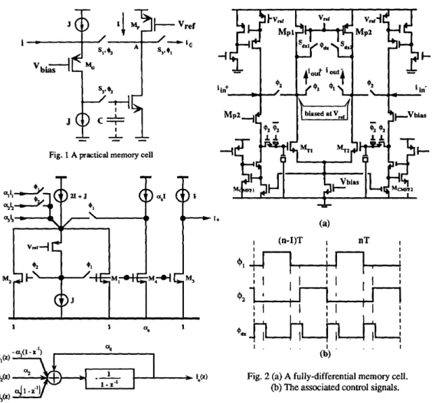
The basic element of the switched-current (SI)
technique is the SI memory cell. To achieve better performance, a practical memory cell is presented as shown in Fig. 1. The grounded-gate voltage amplifier used here comprises the grounded-gate transistor
M,
and two current sources each providing a bias current J. The PMOS transistorM,
with its gate biased at the voltageV,.passes
its drain current equal to I. During phase $2,both
S i andS2
are closed, the signal current i flows into the source of transistor&
and charges the storage capacitorc.
When0-7803-5012-X /99/$10.00 01999 IEEE. 26 1
the current in %reaches I+i and the current in
e
returns to J, equilibrium is established, and the voltage at the summing node A is close to a constant value V,=
Vbiu.+
V,, where vgs is the gate-source voltage of M, with its drain current equal to J. During phase $1, S 3 is closed. The output current io flows into next cascaded connected cell, and the output voltage of the driving cell is fixed at the input node of the driven cell. Since the output node is held close to V,, the memory transistorMT
sustains its current at I+i and gives an output io equal to -i. The grounded-gate amplifier creates a “virtual e a r t h at the input node[6]
(and the output node ,while connecting to the next cascaded cell). In Fig. 2. a fully differential version of the memory cell is illiustrated. To minimize the error current generated into the storage node due to loading effect, high-performance regulated-gate cascode current sources [7] are adopted. The feedback connection to the transistors M,,, andqMm2
provides overall common- mode stability. For glitch reduction, two additional switches Sdx,. and SdxZ are employed to minimize the deviation of signals due to transient glitches. During the non-overlapped period of the clock, both S,, and S , are tumed on, and the difference of the drain currents betweenM, and
M,
is sinked or sourced by the constant voltage source Vrcr During the output phase $1, the switches remain close for a short time to stabilize the output voltage. This can effectively eliminate the unbalance of the drain currents ofM,
and M, during the non-overlapped period thus reduce the glitches at the moment of either41
or $2 goes high.
3.
A Universal Switched-Current Integrator
A universal SI integrator which performs an identical algorithm to a well known switched-capacitor universal integrator is presented[9].
This switched-current universal integrator are duals of those already used in active-RC and switched-capacitor systems. Fig. 3 shows the configuration of the SI universal integrator and the associated circuit is given in Fig.4.
Although identical circuit topology is adopted with respect to that in [9], the presented integrator uses a high-quality meomory cell and has better analog performance. The input currents weighteda l , az
anda,
are accomplished by scaling the aspect ratios (W/L) of the corresponding output transistors and the output stage has unit weight. As derived in[9],
the current equation is given aswhere A,
=
aJ(1
+
a4),
4
=az/(l
+
a4),
4
=
a3/(l
+
4.
General
First
and Second Order
Building Blocks
A. General First-order Building Blocks
function is given by
The general continuous-time first-order transfer
H(s) =
-
a,s+a, (2)S + O ,
The numerator coefficients,
a,,
and a,, determine the type of filter (e.g., low-pass, high pass, and all-pass). Using ihe bilinear transformation (s = (2/r>( 1-
z-1)/(1+
z-1)) in Eq.(2) gives the zdomain transfer function:
1 -=-I
(3
1
=
K.
-
1 - pz-'
where K = (2al+a,,T)/(2aOT), a = (2al-%T)/(2a,+a,,T), iind
p
= (2-w0T)/(2+oOT). Consider the universal SI integratorin Fig. 3. If 2a,- aoT 2 0,
a
2 0, by setting i, = i, =: -i.and i, = 0, the zdomain transfer function becomes,
(4)
Comparison between Eqs. (3) and (4) yields
( 5 )
If 2al- a,,T < 0, a < 0. by setting i, = 4, = i, and i, := 0, the zdomain transfer function becomes,
where A,
=
-
aK,
A,andB
areas
definedin Eq.
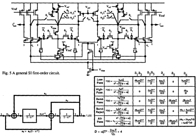
(6). The z-domain transfer functions of Eqs. (4) and (6) thus correspond to those of the general first-order building blocks. Figure 5 shows the general first-order section configuration made of the universal SI circuit.B . General Second-order Building Blocks
The general biquadratic transfer function is given by
with the building block given in Fig. 6. Also, the coefficients associated with every types of filters are summarized in Table 1.
C. Pevormance Verijicatwn
To venfy the operation of the proposed first-order and second-order blocks. a first-order low pass filter and a second order 0.5-dB ripple Chebyshev low-pass filter are relaized respectively. For the first-order LP filter with DC
gain=l, 3dB frequency f F lMHz, its magnitude response is plotted in Fig. 7.
For the secondader
LP
filter, the specifications of the simulated SI filter are given in the sampled-data domain: the ripple bandwidth fp = 500 kHz and the sampling frequency fclk = 5 MHz. Figure 8 shows the theoretical magnitude response and the simulation result with HSPICE. It can be seen that the simulated response agrees closely with the theoretical one for both cases.5.
Case Study: A Cascade Design
Example
To show a design example, a fiith-order 1 dB-ripple Cheby- shev low-pass filter is realized by cascading two biquadratic and one fust-order sections. The specification of this test filter are given in the sampled-data domain: the ripple frequency f = 500 kHz and the sampling frequency fclk = 5 MHz. Following the precedure described in Section 4, the weights of the constituent sections can be determined. Theoretical and simulated magnitude responses of the filter is plotted in Fig. 9. It can be seen that the simulation result of the frequency response characteristics is in close agreement with the theoretical result.In conclusion, a high-performance
SI
memory cell circuit has first been presented. This memory cell circuit utilizes active negative feedback to improve transmission accuracy. Fully differential structures with common-mode feedback are used to reduce charge injection errors. Furthermore, additional glitch reduction switches are employed to improve transient behavior. Based on the proposed cell circuit, a universal SI integrator has been generated which performs an identical algorithm to a well known SC general integrator. General first and second order building blocks which correspond to the bilinear s-z transformation of the general continuous-time first and second order section have been developed from the universal SI integrator. These building blocks are used for designing cascade SI filters. To verify the circuit technique. test filters including a first order low-pass filter, a second order Chebyshev low-pass filter; and a fifth-order Chebyshev low-pass filters have been realized and simulated with HSPICE. The simulation results of the frequency response characteristics show pretty good agreement with the theoretical results.References
[l] J. B. Hughes et al., IEEE ISCAS, p. 1584, 1989. [2] S. J. Daubert et al.J E E Proceedings, vol. 137, pt G, p. [3] G. Wegmann et al., IEE Proceedings, vol. 137. p t G, p. [4] T. S. Fiez et al,, IEEE JSSC, vol. 26, p. 192, 1991.
[SI
R.
H. &le et al., IEEE JSSC, vol. 29, p. 203, 1994. [6] J. B. Hughes et al., IEEE JSSC, vol. 29, p. 1388, 1994. [7] M. Goldenberg et al., IEEE JSSC, vol. 29, p. 1388, 1994. [8] P. J. Crawley et al., IEEE T-CAS, vol. 41, p. 73-86, 1994.[9] C. Toumazou et al., Analog IC Design: the Current- Mode
109,1990. 95,1990.
Approach. London: Peter Peregrinus. 1990.
i
Fig. 1 A practical memory cell
+ i o
1 1 a. 1
I.$)
Fig. 3 Configuration of the SI universal integrator.
I I
7
5 , 3
I . . . . .cd,
' IFig. 2 (a)
Afully-differential memory cell.
(b)
The associated control signals.
Fig.4
Afully-differential circuit
of
Fig.3.
Fig.
5A general SI first-order circuit.
I
as + &(l
-
2.')D
= d T 2 - X . 4Qo
Fig. 6 A general second-order building block.
Table
1Coefficients for various types of filters based on the
second-order block in Fig. 6.
Frequency
(kHz)
Fig. 7 Magnitude response of a
first-order low pass filter.
10