This content has been downloaded from IOPscience. Please scroll down to see the full text.
Download details:
IP Address: 140.113.38.11
This content was downloaded on 25/04/2014 at 04:23
Please note that terms and conditions apply.
Simulation of characteristic variation in 16 nm gate FinFET devices due to intrinsic parameter
fluctuations
View the table of contents for this issue, or go to the journal homepage for more 2010 Nanotechnology 21 095203
(http://iopscience.iop.org/0957-4484/21/9/095203)
IOP PUBLISHING NANOTECHNOLOGY
Nanotechnology 21 (2010) 095203 (7pp) doi:10.1088/0957-4484/21/9/095203
Simulation of characteristic variation in
16 nm gate FinFET devices due to intrinsic
parameter fluctuations
Yiming Li
1,2,3, Chih-Hong Hwang
1and Ming-Hung Han
11Institute of Communication Engineering, National Chiao-Tung University, Hsinchu 300,
Taiwan
2Department of Electrical Engineering, National Chiao-Tung University, Hsinchu 300, Taiwan 3National Nano Device Laboratories, Hsinchu 300, Taiwan
E-mail:[email protected]
Received 16 October 2009, in final form 13 January 2010 Published 3 February 2010
Online atstacks.iop.org/Nano/21/095203
Abstract
High-κ/metal-gate and vertical channel transistors are well-known solutions to continue the device scaling. This work extensively explores the physics and mechanism of the intrinsic parameter fluctuations in nanoscale fin-type field-effect transistors by using an experimentally validated three-dimensional quantum-corrected device simulation. The dominance fluctuation sources in threshold voltage, gate capacitance and cutoff frequency have been found. The emerging fluctuation source, workfunction fluctuation, shows significant impacts on DC characteristics; however, its impact is reduced in AC characteristics due to the screening effect of the inversion layer. Additionally, the channel discrete dopant may enhance the electric field and therefore make the averaged cutoff frequency of fluctuated devices larger than the nominal value of cutoff frequency.
(Some figures in this article are in colour only in the electronic version)
1. Introduction
As the dimensions of semiconductor devices continue to be reduced, device variability is pronounced [1–8]. Fin-type field-effect transistors (FinFETs) [7–9] and high-κ/ metal-gate technology [10] are promising for semiconductor manufacturing. However, the use of metal as a gate material may introduce additional random fluctuations, workfunction fluctuation (WKF), due to the uncontrollable grain orientations of metal during the growth period. The WKF-induced threshold voltage (Vth) fluctuation on planar MOSFETs
has been reported [10]. The different orientations of crystal structure may have different surface densities and workfunctions [11]. Since the device gate area is thus composed of a number of grains with different workfunctions, the workfunction and threshold voltage of the device are probabilistic distributions rather than deterministic values.
In studying characteristic fluctuations of FinFETs, diverse approaches have recently been presented [7,8]; however, they only focused on the random-dopant fluctuation (RDF) and
process-variation effect (PVE) on device DC characteristics, such as Vth and current fluctuation. The effects of WKF
on FinFET and these intrinsic parameter fluctuations on AC characteristics are not clear. Thus, a comprehensive understanding of the intrinsic parameter fluctuations on FinFETs is required. This study extensively explores the intrinsic device parameter fluctuations (WKF, PVE and RDF) on 16 nm gate silicon-on-insulator (SOI) FinFETs by an experimentally validated three-dimensional quantum-corrected device simulation [4]. Both the current–voltage characteristics and the physical models of FinFET have been calibrated with experimentally fabricated FinFETs [9]. The major variability sources in DC and AC characteristics of FinFETs are provided for the first time. This study explores the fluctuations on FinFET devices, which can in turn be used to optimize the reliability of nanoscale systems.
This paper is organized as follows. Section2introduces the simulation technique for studying the effect of intrinsic parameter fluctuations in nanoscale devices and circuits. Section3studies the characteristic fluctuations in 16 nm gate
Nanotechnology 21 (2010) 095203 Y Li et al
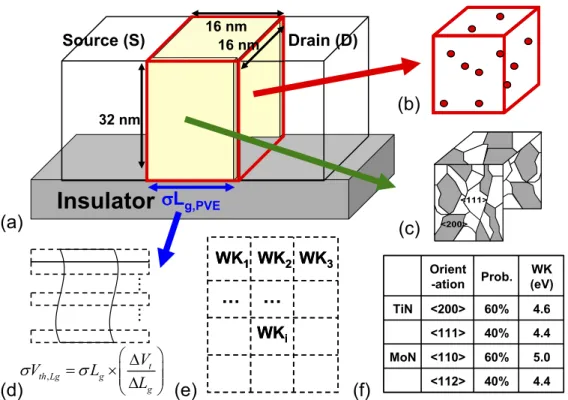
Figure 1. (a) An illustration of the explored SOI FinFETs with (b) random-dopant fluctuation, (d) process-variation effect and
(c) workfunction fluctuation. The number of channel dopants in the device may vary from 2 to 22, and the average number is 13. (d) The discretization scheme for estimating PVE-inducedσ Vthand the calculation formula. (e) The estimation of workfunction fluctuation. The gate
area is partitioned into several pieces according to the average grain size. The workfunction of each partitioned area (WKi) is then randomized
according to the probability distribution in (f). The effect workfunction of a single device is obtained and used from estimation of workfunction-variation-induced fluctuation.
devices and circuits. Finally, conclusions are drawn and future work is suggested.
2. The statistical simulation technique
Figure 1(a) illustrates the explored 16 nm gate SOI FinFETs with amorphous-based TiN/HfSiON gate stacks with an equivalent oxide thickness (EOT) of 1.2 nm [10]. The equivalent channel doping concentration is 1.48 × 1018cm−3. To compare them on the same basis, the device dimension and Vth for both n- and p-type devices are the same. Figure1(b)
illustrates the RDF effect in transistors, where the simulation scenario mainly follows our recent work [4,7]. The device simulation is performed by solving a set of three-dimensional ‘atomistic’ drift–diffusion equations with quantum corrections by the density gradient method [4, 7, 12, 13]. Note that, in ‘atomistic’ device simulation, the resolution of individual charges within classical device simulation using a fine mesh creates problems associated with singularities in the Coulomb potential [5, 6]. The potential becomes too steep with a fine mesh and therefore the majority carriers are unphysically trapped by ionized impurities and the mobile carrier density is reduced [5, 6]. Thus, the density gradient approximation is used to handle discrete charges by properly introducing the quantum mechanical effects [4,7,12,13].
The mobility model is quantified with our device measurements for the best accuracy and the characteristic fluctuation has been validated with the experimentally
measured DC base band data [4,9]. The device simulation is performed by solving a set of 3D drift–diffusion equations with quantum corrections by the density gradient method [4, 7, 12, 13], which is conducted using a parallel computing system [14]. The mobility model used in the device simulation, according to Matthiessen’s rule [15], can be expressed as 1 μ = D μsurf aps + D μsurf rs + 1 μbulk , (1)
where D = exp(x/lcrit), x is the distance from the interface
and lcrit is a fitting parameter. The mobility consists of three
parts: (1) the surface contribution due to acoustic phonon scattering μsurf aps = (B/E) + [C(Ni/N0)τ/E1/3(T/T0)K],
where Ni = NA + ND, T0 = 300 K, E is the transverse
electric field normal to the interface of semiconductor and insulator, B and C are parameters which are based on physically derived quantities, N0andτ are fitting parameters,
T is lattice temperature and K is the temperature dependence of the probability of surface phonon scattering; (2) the contribution attributed to surface roughness scattering is
μsurf rs = ((E/Eref)χ/δ + E3/η)−1, whereχ = A + α(n +
p)Nref/(Ni + N1)ν, Eref = 1 V cm−1 is a reference electric
field to ensure a unitless numerator inμsurf rs, Nref = 1 cm−3
is a reference doping concentration to cancel the unit of the term raised to the power v in the denominator of χ, δ is a constant that depends on the details of the technology, 2
Nanotechnology 21 (2010) 095203 Y Li et al
Figure 2. The ID–VGcharacteristics for (a) n-type and (b) p-type SOI FinFETs. The insets are the components ofσ Vth, in which the drain
bias is 1 V.
such as oxide growth conditions, N1 = 1 cm−3, and A
and η are fitted field-dependent coefficients. α is a fitting parameter for doping concentration (3) and the bulk mobility is μbulk = μL(T/T0)−ξ, where μL is the mobility due to
bulk phonon scattering and ξ is a fitting parameter for the temperature dependence of mobility. The mobility model is quantified with our device measurements for the best accuracy and the characteristic fluctuation has been validated with the experimentally measured DC base band data [4].
The PVE includes gate length deviation (σ Lg) and line
edge roughness (σLER) whose magnitude follows the ITRS
roadmap that 3σ Lg = 0.7 nm and 3σLER = 0.8 nm
for the 16 nm technology node [16]. The equation of figure1(d) presents the estimation formula andσ Lgandσ Vth
are obtained from the Vth roll-off curve. As the PVE-induced
gate length variation (σ Lg,PVE) is obtained, the PVE-induced
Vth fluctuation (σ Vth,PVE) is calculated by characteristics of
the Vthroll-off. The detailed simulation techniques for RDF
and PVE simulation follow our previous works [17–25]. For WKF, a statistically sound Monte Carlo simulation approach is advanced, as shown in figure 1(e). Based on the average grain size of 4 nm [10], the gate area is first partitioned into several parts. Then, the workfunction of each partitioned area (W Ki) is randomized following the properties of metal
in figure 1(f) [11]. We herein use titanium nitride (TiN) and molybdenum nitride (MoN) as gate material for NMOS and PMOS transistors, respectively. After partition and randomization, the effective device workfunction of a single transistor is then obtained and used for estimation of WKF-induced Vth fluctuation (σ Vth,WKF). Notably, the different
processes of gate formulation, gate first or replacement gate may change the thermal budget and change the grain size of the metal material.
3. Result and discussion
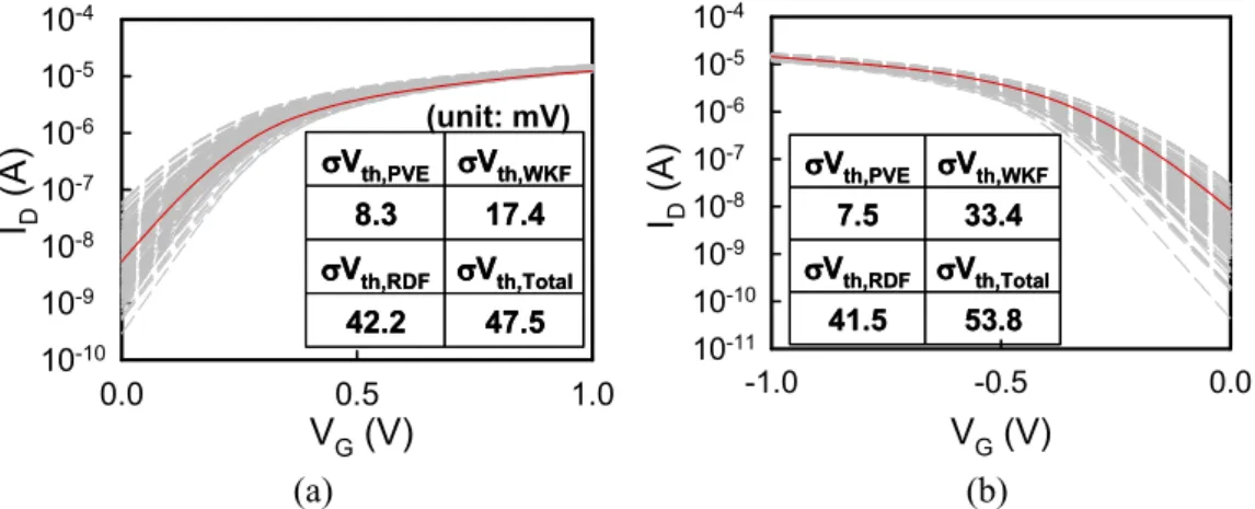
Figures 2(a) and (b) show the characteristics of the drain current (ID) versus the gate voltage (VG). The solid lines are the
nominal case with supposed device dimensions, workfunction
and doping concentration; the dashed lines are cases with intrinsic parameter fluctuations. The insets of figures 2(a) and (b) show theσ Vth for n-type and p-type FinFETs. The
total threshold voltage fluctuation (σ Vth,Total) is obtained by
statistical addition of variances, (σ Vth,Total)2≈ (σ Vth,WKF)2+
(σ Vth,PVE)2+(σ Vth,RDF)2. In SOI FinFETs, the RDF and WKF
dominate theσ Vth in both n-type and p-type transistors. The
σ Vth,WKFin p-type FinFETs becomes comparable toσ Vth,RDF
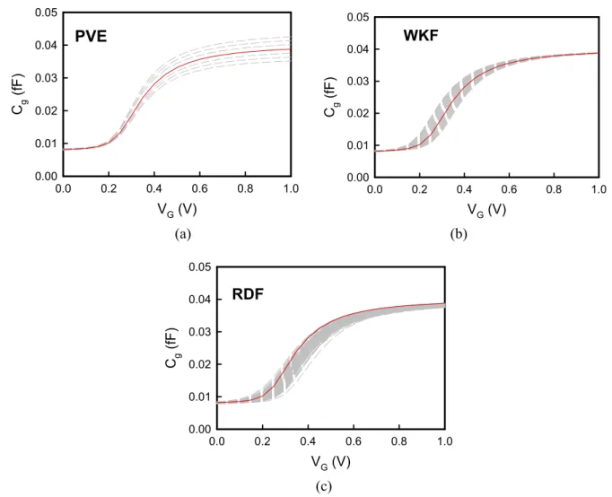
due to the large deviation of workfunction, which implies the importance of workfunction fluctuation in nanoscale device with scaled gate area. Notably, the statistical addition of individual fluctuation sources herein simplifies the variability analysis of nanodevices significantly [3]. It is believed that the dominant source of fluctuation will not be significantly altered. The WKF-, PVE-and RDF-fluctuated Cg are presented
in figures 3(a)–(c), where the solid line shows the nominal case with 16 nm gate, 1.48 × 1018cm−3 channel doping
and the dashed lines are fluctuated cases. The different intrinsic parameter fluctuations induced rather different Cg–
VG characteristics. Figure4summarizes the gate capacitance
fluctuations (σCg) with 0, 0.5 and 1.0 V gate bias. Different
to the results of the Vth fluctuation, the WKF brought less
impact on gate capacitance fluctuation. At low gate bias or negative gate bias, the accumulation layer screens the impact of WKF. Additionally, at low gate bias, the total capacitance decreases because of the increased depletion region. The associated value of Cg fluctuation is small. The capacitive
response is then dominated by the increment of inversion in the moderate inversion. The device characteristics are then impacted by the intrinsic parameter-fluctuated electrostatic potentials. If the high VG is achieved, the capacitive response
becomes dominated by the inversion layer and the impact of the individual dopants on the device electrostatics is screened by the inversion layer itself. The variation of capacitance now again becomes the variation of gate oxide. The impact of WKF-induced electrostatic potential variations is therefore bringing less impact on the channel surface. Our preliminary results show that the RDF and PVE dominate the gate capacitance fluctuations at all gate bias conditions, respectively. The impacts of the WKF on Cg is reduced
Nanotechnology 21 (2010) 095203 Y Li et al
Figure 3. The Cg–VGcharacteristics for the explored devices with (a) PVE, (b) WKF and (c) RDF.
significantly at high gate voltage (VG) due to the screening
effect of the inversion layer of the device, which screens the variation of surface electrostatic potential and decreases the fluctuation of gate capacitance. The screening effect resulting from the inversion layer also decreases the RDF-induced gate capacitance fluctuation at high gate bias; however, the screening effect of the inversion layer is weakened by discrete dopants positioned near the channel surface. Notably, the PVE brings direct impact on gate length and therefore influences the gate capacitance. The PVE-induced gate capacitance fluctuation is independent of screening effect and should be noticed when the transistor operated in high gate bias, as shown in figure4.
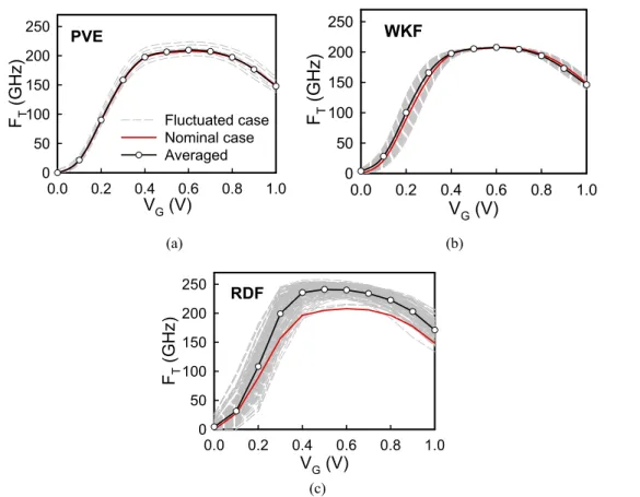
Figures 5(a)–(c) describe the PVE-, WKF-, and RDF-induced characteristic fluctuation of the cutoff frequency (FT = vsat/2π Lg = gm/2πCg) for the n-type transistors,
where gmandvsat are the transconductance and the saturation
velocity, respectively. The solid lines are the nominal case; the dashed lines are the cases with intrinsic parameter fluctuation; the symbol lines are the averaged result. At low VG, the
cutoff frequency of FinFET increases as VG increases due to
the enhancement of carrier velocity. The cutoff frequency is saturated and then degrades in the high electric field due to the velocity saturation and scattering of carriers. The
Figure 4. The Cgfluctuation at VG= 0, 0.5 and 1 V for 16 nm gate
FinFETs with intrinsic parameter fluctuations WKF, PVE and RDF.
PVE-induced σ FT in figure 5(a) is significant in all bias
conditions owing to the direct impact of gate length variation on FT. Different to the PVE-induced σ FT, the
WKF-inducedσ FT, figure5(b), diminished as the velocity saturation
occurs. The inversion layer is formed at this time and 4
Nanotechnology 21 (2010) 095203 Y Li et al
Figure 5. The FT–VGcharacteristics for the explored devices with (a) PVE, (b) WKF and (c) RDF.
screens the variation of surface electrostatic potential induced by WKF. The σ FT then becomes significant at high field
because of the carrier scattering. As for the RDF-induced
σ FT, as shown in figure 5(c), the σ FT does not diminish
when the saturation of the carrier velocity occurs due to the randomness of carrier–impurity scattering events and carrier velocity variation. Moreover, though the screening effect at high field may also reduce the RDF-inducedσ FT, the shielding
effect may be broken by discrete dopants positioned near the channel surface. The RDF-induced σ FT thus dominates the
fluctuation of cutoff frequency. The σ FT is summarized in
figure6, in which the RDF dominates theσ FT. Both the
RDF-and WKF-induced σ FT are significant in the subthreshold
region. Then the σ FT is reduced due to the screening effect
of the inversion layer. The scattering effect occurring in the high-field region then increases theσ FTinduced by RDF.
Notably, our preliminary result shows that the nominal and the averaged values of FT are similar for the results of PVE
and WKF. However, in RDF, the difference of the nominal and the averaged FTbecomes significant as VGincreases. For
the discrete dopants in the channel, the channel dopants will induce a relatively negative potential in the channel and twist the electric field nearby, as plotted in figures7(a) and (b). The arrows in figure7(a) present the direction of the electrical field. Figure7(c) presents the electric field for three cut lines at the channel surface. Line 1 is with one dopant located at channel surface; line 2 is without the impurity at the conducting path; line 3 is also has one dopant located at the channel surface, but the dopant is located 0.5 nm below the channel surface. The result shows that the dopant inside the channel may enhance
Figure 6. The summarizedσ FTfor the explored devices with
(a) PVE, (b) WKF and (c) RDF.
the electric field nearby. The electric field strength is location-dependent and its magnitude decreases as the distance from a location to the dopant increases, as shown in line 1 and line 3 of figure 7(c). The twisted electric field then enhances the electron velocity, vsat, as shown in figure 7(d) and therefore
increases the average value of FT. The average value of FT is
larger than the nominal FT due to the enhanced electric field
near the channel dopants.
4. Conclusions
This study has extensively explored the metal-gate device’s DC and AC variability. The dominant variability sources
Nanotechnology 21 (2010) 095203 Y Li et al
Figure 7. The distributions (a) potential and (b) electric field of the channel for a discrete-dopant-fluctuated transistor. (c) 1D electric field
distribution for three cut lines at channel surface. Line 1 is with one dopant located at channel surface; line 2 is without impurity at the conducting path; line 3 also has one dopant located at channel surface, but the dopant is located 0.5 nm below the channel surface. (d) The distribution of electron velocity, where the velocity is enhanced by electric field near dopants.
in nanoscale FinFETs have been identified. The RDF and WKF are the dominating factors inσ Vthfor n-type and p-type
FinFETs. The large deviation of workfunction difference in PMOS transistors has impacted the device threshold voltage and therefore should be noticed in the nanoscale transistors era. For the device AC characteristics, the influence of the emerging fluctuation source, WKF, is reduced due to the screening effect of the inversion layer. The screening effect is less effective in RDF because the discrete dopant positioned in the channel may break the shielding and induce random scattering events. The RDF therefore dominates theσ FT. The result of this study is
important in understanding the intrinsic parameter fluctuation in DC and AC characteristics, which is useful for nanodevice design in different applications. Currently we are working on the modeling of WKF and developing a fluctuation suppression approach for WKF, such as reduction of grain size.
Acknowledgment
This work was supported by the Taiwan National Science Council (NSC) under contract NSC-97-2221-E-009-154-MY2, and by the Taiwan Semiconductor Manufacturing Company, Hsinchu, Taiwan under a 2008-2010 grant.
References
[1] Wong H-S, Taur Y and Frank D J 1998 Discrete random dopant distribution effects in nanometer-scale MOSFETs
Microelectron. Reliab.38 1447–56
[2] Asenov A 1999 Random dopant induced threshold voltage lowering and fluctuations in sub 50 nm MOSFETs: a statistical 3D ‘atomistic’ simulation study Nanotechnology
10 153–8
[3] Hori M, Shinada T, Taira K, Shimamoto N, Tanii T, Endo T and Ohdomari I 2009 Performance enhancement of semiconductor devices by control of discrete dopant distribution Nanotechnology20 36520
[4] Li Y, Yu S-M, Hwang J-R and Yang F-L 2008 Discrete dopant fluctuated 20 nm/15 nm-gate planar CMOS IEEE Trans.
Electron Devices55 1449–55
[5] Sano N and Tomizawa M 2007 Random dopant model for three-dimensional drift-diffusion simulations in metal-oxide–semiconductor field-effect-transistors Appl.
Phys. Lett.79 2267
[6] Sano N, Matsuzawa K, Mukai M and Nakayama N 2002 On discrete random dopant modeling in drift-diffusion simulations: physical meaning of ‘atomistic’ dopants
Microelectron. Reliab.42 189–99
[7] Li Y and Hwang C-H 2007 Discrete-dopant-induced characteristic fluctuations in 16nm multiple-gate silicon-on-insulator devices J. Appl. Phys.102 084509
[8] Baravelli E, Jurczak M, Speciale N, Meyer K D and
Dixit A 2008 Impact of LER and random dopant fluctuations on FinFET matching performance IEEE Trans. Nanotechnol.
7 291–8
Nanotechnology 21 (2010) 095203 Y Li et al [9] Li Y and Hwang C-H 2007 Effect of fin angle on electrical
characteristics of nanoscale round-top-gate bulk FinFETs
IEEE Trans. Electron Devices54 3426–9
[10] Ohmori K, Matsuki T, Ishikawa D, Morooka T, Aminaka T, Sugita Y, Chikyow T, Shiraishi K, Nara Y and
Yamada K 2008 Impact of additional factors in threshold voltage variability of metal/high-k gate stacks and its reduction by controlling crystalline structure and grain size in the metal gates Int. Electron Device Mtg. Tech. Tech. Dig. pp 1–4
[11] He J L, Setsuhara Y, Shimizu I and Miyake S 2001 Structure refinement and hardness enhancement of titanium nitride films by addition of copper Surf. Coat. Technol.137 38–42
[12] Ancona M G and Tiersten H F 1987 Macroscopic physics of the silicon inversion layer Phys. Rev. B35 7959–65
[13] Roy G, Brown A R, Asenov A and Roy S 2003 Quantum aspects of resolving discrete charges in ‘atomistic’ device simulations J. Comput. Electron.2 323–7
[14] Li Y and Yu S-M 2005 A parallel adaptive finite volume method for nanoscale double-gate MOSFETs simulation
J. Comput. Appl. Math.175 87–99
[15] Darwish M N, Lentz J L, Pinto M R, Zeitzoff P M,
Krutsick T J and Vuong H H 1997 An improved electron and hole mobility model for general purpose device simulation
IEEE Trans. Electron Devices44 1529–38
[16] www.itrs.net/
[17] Li Y and Yu S-M 2006 Comparison of random-dopant-induced threshold voltage fluctuation in nanoscale single-, double-, and surrounding-gate field-effect transistors Jpn. J. Appl.
Phys.45 6860–5
[18] Li Y and Yu S-M 2007 A coupled-simulation-and-optimization approach to nanodevice fabrication with minimization of electrical characteristics fluctuation IEEE Trans. Semicond.
Manuf.20 432–8
[19] Li Y and Hwang C-H 2007 Electrical characteristic fluctuations in 16 nm bulk-FinFET devices Microelectron. Eng.
84 2093–6
[20] Li Y, Yu S-M and Chen C-M 2007 Process-variation- and random-dopants-induced threshold voltage fluctuations in nanoscale CMOS and SOI devices Microelectron. Eng.
84 2117–20
[21] Li Y, Hwang C-H and Huang H-M 2008 Large-scale atomistic approach to discrete-dopant-induced characteristic fluctuations in silicon nanowire transistors Phys. Status
Solidi a205 1505–10
[22] Li Y and Hwang C-H 2008 High-frequency characteristic fluctuations of nano-MOSFET circuit induced by random dopants IEEE Trans. Microw. Theory Tech.56 2726–33
[23] Li Y and Hwang C-H 2008 Discrete-dopant-fluctuated threshold voltage roll-off in sub-16 nm bulk FinFETs Japan.
J. Appl. Phys47 2580–4
[24] Li Y, Hwang C-H and Li T-Y 2009 Discrete-dopant-induced timing fluctuation and suppression in nanoscale CMOS circuit IEEE Trans. Circuits Syst. II56 379–83
[25] Li Y, Hwang C-H and Li T-Y 2009 Random-dopant-induced variability in nano-CMOS devices and digital circuits IEEE