Optically modulated internal strain in InGaN
quantum dots grown on SiN
x
nano masks
H. J. Chang1, T. T. Chen1, L. L. Huang1, and Y. F. Chen1 J. Y. Tsai2, T. C. Wang2, and H. C. Kuo2
1Department of Physics, National Taiwan University, Taipei 106, Taiwan 2Institute of Electro-optical Engineering, National Chiao-Tung University,
Hsin-Tsu 300, Taiwan
Abstract: Optically modulated internal strain has been observed in InGaN quantum dots (QDs) deposited on SiNx nano masks. The modulated internal strain can induce a number of intriguing effects, including the change of refractive index and the redshift of InGaN A1(LO) phonon. The underlying mechanism can be well accounted for in terms of the variation of internal strain through the converse piezoelectric effect arising from the screening of the internal electric field due to spatial separation of photoexcited electrons and holes. Our results point out a convenient way for the fine tuning of physical properties in nitride-based semiconductor nanostructures, which is very important for high quality optoelectronic devices.
©2006 Optical Society of America
OCIS codes: (300.6450) Spectroscopy, Raman; (250.5230) Photoluminescence.
References and links
1. S. Nakamura and G. Fasol, The Blue Laser Diode (Springer, Berlin, 1997).
2. H. Morkoc, S. Strite, G. B. Gao, M. E. Lin, B. Sverdlov, and M. Burns, “Large-band-gap SiC, III-V nitride, and II-VI ZnSe-based semiconductor device technologies,” J. Appl. Phys. 76, 1363-1398 (1994).
3. S. Nakamura, M. Senoh, S. Nagahama, N. Iwasa, T. Yamada, T. Matsusshita, H. Kiyoko, and Y. Sugimoto, “InGaN-Based Multi-Quantum-Well-Structure Laser Diodes,” Jpn. J. Appl. Phys. 35, L74-L76 (1996). 4. M. Sugisaki, H. W. Ren, S. V. Nair, K. Nishi, and Y. Masumoto, “External-field effects on the optical
spectra of self-assembled InP quantum dots,” Phys. Rev. B 66, 235309 (2002).
5. S. Raymond, J. P. Reynolds, J. L. Merz, S. Fafard, Y. Feng, and S. Charbonneau, “Asymmetric Stark shift in AlInAs/AlGaAs self-assembled dots,” Phys. Rev. B 58, R13415-R13418 (1998).
6. M. Sugisaki, H.-W. Ren, S.V. Nair, K. Nishi, S. Sugou, T. Okuno, and Y. Masumoto, “Optical anisotropy in self-assembled InP quantum dots,” Phys. Rev. B 59, R5300-R5303 (1999).
7. P. Michler, A. Kiraz, C. Becher, W. V. Schoenfeld, P. M. Petroff, L. Zhang, E. Hu, and A. Imamoğlu, “A quantum dot single-photon turnstile device,” Science 290, 2282-2285 (2000).
8. C. Santori, M. Pelton, G. Solomon, Y. Dale, and Y. Yamamoto, “Triggered single photons from a quantum dot,” Phys. Rev. Lett. 86, 1502-1505 (2001).
9. J. Shi, C. Xia, S. Wei, and Z. Liu, “Exciton states in wurtzite InGaN strained coupled quantum dots: Effects of piezoelectricity and spontaneous polarization,” J. Appl. Phys. 97, 083705 (2005).
10. J. F. Nye, Physical Properties of Crystals, (Oxford, University Press, London, 1972).
11. A. Shikanai, T. Deguchi, T. Sota, T. Kuroda, A. Tackeuchi, S. Chichibu, and S. Nakamura, “A pump and probe study of photoinduced internal field screening dynamics in an AlGaN/GaN single-quantum-well structure,” Appl. Phys. Lett. 76, 454- 456 (2000).
12. R. C. Tu, C. J. Tun, C. C. Chuo, B. C. Lee, C. E. Tsai, T. C. Wang, J. Chi, C. P. Lee and G. C. Chi, “Ultra-High-Density InGaN Quantum Dots Grown by Metalorganic Chemical Vapor Deposition,” Jpn. J. Appl. Phys. 43, L264-L266 (2004).
13. F. Della Sala, A. Di Carlo, P. Lugli, F. Bernardini, V. Fiorentini, R. Scholz, and J.-M. Jancu, “Free-carrier screening of polarization fields in wurtzite GaN/InGaN laser structures,” Appl. Phys. Lett. 74, 2002-2004 (1999).
14. D. C. Marra, E. S. Aydil, S. J. Joo, E. Yoon, and V. I. Srdanov, “Angle-dependent photoluminescence spectra of hydrogenated amorphous silicon thin films,” Appl. Phys. Lett. 77, 3346-3348 (2000).
15. C. H. Chen, W. H. Chen, Y.F. Chen, and T. Y. Lin, “Piezoelectric, electro-optical, and photoelastic effects in InGaN/GaN multiple quantum wells,” Appl. Phys. Lett. 83, 1770-1772 (2003).
16. H. J. Chang, C. H. Chen, L. Y. Huang, Y. F. Chen, and T. Y. Lin, “In-plane optical anisotropy in
17. A. G. Kontos, Y. S. Raptis, N. T. Pelekanos, A. Georgakilas, E. Bellet-Amalric, and D. Jalabert, “Micro-Raman characterization of InGaN/GaN/Al2O3 heterostructures,” Phys. Rev. B 72, 155336 (2005).
18. V. Darakchieva, P. P. Paskov, E. Valcheva, T. Paskova, B. Monemar, M. Schubert, H. Lu, and W. J. Schaff, “Deformation potentials of the E1(TO) and E2 modes of InN,” Appl. Phys. Lett. 84, 3636-3638
(2004).
19. F. C. Wang, C. L. Cheng, Y. F. Chen, C. F. Huang, and C. C. Yang, “Residual thermal strain in thick GaN epifilms revealed by cross-sectional Raman scattering and cathodoluminescence spectra,” Semicond. Sci. Technol. 22 896–899 (2007).
1. Introduction
The group III-nitride wide-band-gap semiconductors have been recognized as very important materials for many optoelectronic devices, such as blue ultraviolet (UV) light emitting diodes (LEDs), laser diodes (LDs), and high-temperature/high-power electronic devices [1-3]. InGaN/GaN quantum wells (QWs) structures have successfully been used as the active layers in LEDs and LDs [1-3]. However, the threshold current density is still high for LDs with InGaN QWs structures. It is expected that using quantum dots (QDs) instead of QWs as the active layer can improve the performance of LDs. It is well known that QDs areable to confine carriers in all three spatial dimensions, and display discrete energy levels analogous to thoseof an atom. A number of physical phenomena observed inatomic physics have also been seen in QDs, including the quantum-confined Stark effect (QCSE) [4,5], strong optical anisotropy [6], as well as photon anti-bunching [7,8]. The study of the QCSE is important both for fundamental physics and device applications, such as in electro-optical modulators, light-emitting devices, and quantum information technology. In wurtzite structural InGaN QDs, due to the existence of a strong piezoelectric (PZ) field, they possess many peculiar features, such as giant optical anisotropy as well as the strong QCSE induced by built-in PZ field [9,10]. Therefore, the influence of the PZ field on the properties of InGaN quantum structures has attracted a great deal of attention. While the potential applications of optoelectronic devices based on nitride QDs are quite high, the work demonstrating the significance of the optical modulation on the PZ field is still very limited. In this paper, we report the observation of photoinduced internal field screening in InGaN QDs, which produces several intriguing effects. It is found that the reduction in the refractive index can be modulated by the optical excitation density. From the micro-Raman scattering measurements, the InGaN A1(LO) phonon shows a redshift in frequency with increasing optical excitation density. Based on the converse PZ effect [11], all our results can be well understood, in which the built-in PZ field is screened by the spatial separation of photoexcited electrons and holes, and the internal residual strain is therefore reduced. These results not only evidence the possibility of the optically modulated internal strain effect in InGaN QDs, but also provide a convenient way to manipulate the optical properties, which should be very useful for the application of optoelectronic devices.
2. Experiment
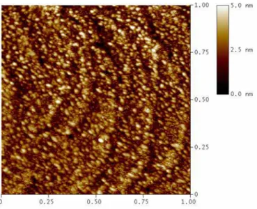
The studied ultra-high-density In0.2Ga0.8N QDs were grown by metalorganic chemical vapor deposition (MOCVD). A 30 nm-thick un-doped GaN layer was first deposited on c-face sapphire substrates at 550 °C, followed by a 2-μm-thick Si-doped GaN underlying layer at 1000 °C. Then, NH3 and the diluted Si2H6 were flowed through the sample to grow a rough SiNx layer on the n-type GaN underlying layer with increasing the SiNx treatment time to 195 s. The temperature was then ramped down to 800 °C to grow the In0.2Ga0.8N layers, and a 10 nm un-doped GaN cap layer was grown on the InGaN layer to complete the sample structure. Atomic force microscopy (AFM) images of the uncapped sample are shown in Fig. 1. The average widths, heights, and densities of QDs in the samples are estimated to be about 35 nm, 2.46 nm, and 2.9×1011 cm-2, respectively. A detailed description of the growth process has been published elsewhere [12].The PL measurements were performed with a SPEX 0.85 m monochromator. The chopping frequency for AC measurements is 100 Hz. A cw He-Cd laser with a wavelength of 325 nm was used for PL excitation, and the spot size was focused to about 1000 μm2 on the sample surface. A cooled GaAs photomultiplier tube interfaced with a
lock-in amplifier was used as a detector. The resolution of the PL spectra is about 0.5 nm. The edge PL spectra were collected along edge direction of the sample. The μ-Raman scattering spectra were measured by a Jobin-Yvon T64000 system at room temperature using a He-Cd laser with a 325 nm in backscattering geometry. The incident and scattered light were parallel to the c axis, which in turn was normal to the growth surface.
Fig. 1. Atomic force microscope images of InGaN layers with 195 s of SiNx treatment on the
underlying GaN layers.
3. Results and discussion
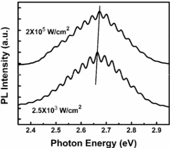
Figure 2 displays the edge PL spectra for InGaN QDs excited with optical excitation density ranging from 2.5x10³ to 2x10⁵ W/cm2. It was apparent that both of the edge PL spectra are dominated by a strong emission with a pronounced interference pattern. The main peak position of the edge PL spectra shows a blueshift as the optical excitation density increases, which can be well explained by the QCSE. For the lattice mismatched InGaN/GaN heterostructure, a built-in PZ field is induced since group III nitrides have large piezoelectric constants along the (0001) orientation [13]. The PZ field can tilt the bandedge and spatially separate the photoexcited electrons and holes, which result in the observation of the QCSE. Because the induced field caused by the photoexcited carriers is opposite to the PZ field. Consequentially, the increase of the excitation power enhances the screening of the PZ field, weakens the QCSE, and then increases the transition energy, resulting in a blueshift.
The pronounced features of the edge PL spectra seen in Fig. 2 can be explained in terms of the interference phenomenon occurring in a Fabry-Pérot microcavity. The interference pattern follows the Fabry-Pérot equation [14], mλ = 2dncosΨ, where m is the interference order, λ is the wavelength of propagation radiation, d is the thickness, n is the refractive index, and Ψ is the wave-front propagation angle with respect to the surface normal. For a fixed angle and a light source, there will be a set of allowed wavelength that satisfiesthe Fabry-Pérot equation, each associated with a cavity mode. This behavior has been widely used to measure very small changes inrefractive index [15, 16]. Indeed, a number of promising sensitive devices based on optical interference effects have emerged recently. As we can see that the interference pattern shifts with the change of the incident light density, it therefore provides an excellent opportunity to accurately determine the refractive index by using the Fabry-Pérot equation with a fixed thickness d of the nitride semiconductor layers. Figure 3 shows the refractive index as a function of the optical excitation density, which clearly shows that an increased excitation power density results in a reduction of the refractive index. Here, the total thickness d~2 μm of all the nitride layers deposited on the sapphire substrate has been used in
the calculation. Since no external electric field or external pressure is applied in the measurements, the responsible mechanism for the refractive index changes should arise from the internal effects existing in the InGaN QDs. A positive quantity of the refractive index changes (∆ n) between the strained and the relaxed layers isexpected due to the internal PZ field being in the(0001) direction and the compressive strain in InGaN QDs.Because the PZ field in InGaN QDs is screened by the photoexcited electrons and holes, it leads to a reduction of the internal strain. Thus, a smaller refractive index of the less strainedQDs is produced via the optically modulated internal strain effect. Apparently, when a higher excitation density is applied to the QDs, the screeningof the PZ field isenhanced, the internal strain decreases, and then the refractive index becomes smaller. This behavior provides a reminiscence of the well-known phenomenon called photoelastic effect, which is referred to the change in the internal strain of a material due to an incident light beam [10].
Fig. 2. Edge photoluminescence spectra of InGaN quantum dots (QDs) with different excitation density at room temperature. A guiding line is used to show the blueshift with increasing the pumping power.
Fig. 3. Refractive index as a function of the optical excitation density. The refractive index was calculated from the interference pattern shown in Fig. 2 by using the Fabry- Pérot equation listed in the text.
Figure 4 shows the PL peak position of InGaN QDs as a function of temperature under high and low excitation intensity. Under high excitation intensity, the PZ field is severely screened and the PL temperature dependence is similar to that of bulk material, i.e., the band gap decreases with increasing temperature. On the other hand, under low excitation intensity, a blueshift in the PL peak is observed when temperature increases from 20 K to 90 K. We can also understand this abnormal PL blueshift based on the screening of the PZ field due to
thermal excitation. At low temperature, carriers are frozen in localized centers, and they will be thermally activated as temperature increases. This process will induce partial screening of the PZ field and lead to the observed blueshift in the PL spectra. The temperature dependent PL spectra thus reflect a competition between the blueshift induced by the thermal screening of the PZ field and the redshift induced by electron-phonon interaction.
Fig. 4. Temperature dependence of the photoluminescence peak position of InGaN QDs under high and low excitation intensity.
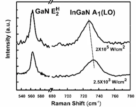
To further elucidate the photoinduced internal field screening behaviors in InGaN QDs, we have performed micro-Raman scattering measurements. In Fig. 5, we show the room-temperature micro-Raman scattering spectra with optical excitation density ranging from 2.5 X 10³ to 2 X 10⁵ W/cm2. The Raman spectra were recorded with the incident light parallel to the c-axis in the backscattering geometry. In this configuration, only A1(LO) and E2 are allowed modes for the wurzite-type crystals according to the Raman selection rules. Thus the peak at 565 cm-1 corresponds to E2H mode of the strained GaN layer, while the broaden line located near 730 cm-1 corresponds to A1(LO) mode of InGaN QDs, respectively [17].
Figure 6(a) shows the A1(LO) and E2H phonon modes as a function of optical excitation density. It displays that the shift of the A1(LO) peak decreases in energy with increasing excitation density, while the peak of the GaN E2H mode remains unchanged. There are two possible mechanisms that can induce the phonon peak shift of InGaN QDs in our study: (i) laser-induced heating in nanostructure ensembles; (ii) photogenerated carriers induced screening of the PZ field. The laser-induced heating effect can be easily ruled out, because the observed GaN E2H mode does not change with the variation of incident pumping power. Therefore, the most likely mechanism responsible for the observed A1(LO) mode shift is the photoelastic effect as described above. Here, we emphasize again that due to the spatial separation of photoexcited electrons and holes, the internal electric field is screened and becomes smaller. Though the converse piezoelectric effect, the internal strain is therefore reduced. Because of the reduction of the internal strain, a redshift in the frequency of the A1(LO) phonon is expected. The decrease in the frequency of A1(LO) mode implies that a uniaxial tensile strain along the c-axis and hence a biaxial compressive strain in the c-plane both exist in the QDs. Increasing excitation density will enhance the screening of the PZ field, which will lead to a smaller compressive strain, and then a smaller A1(LO) mode frequency.
To estimate the magnitude of the strain under different pumping density, we use the following equation [19]
⎥
⎦
⎤
⎢
⎣
⎡
⎟⎟⎠
⎞
⎜⎜⎝
⎛
−
Δ
=
33 132
/
C
C
b
a
ω
ε
, (1)where ε is the biaxial strain, Δω is the deviation in frequency of the A1(LO) phonon, a and b are phonon deformation potentials, and C13 and C33 are elastic constants, respectively. Figure 6(b) shows the strain as a function of excitation density according to the calculation based on Eq. (1), where the deformation potentials a, b and the elastic constants C13, C33 were estimated by the extrapolation of the data for AlN and InN [17]. The value of the calculated strain is in the same order of magnitude reported previously [17]. Evidently, with increasing excitation power, the value of ε increases from -1.3% to -0.5% which implies a reduced biaxial compressive strain in the QDs. Additionally, it is known that the decrease of the biaxial compressive strain will result in a decreased transition energy [19]. However, the PL peak energy displays a blueshift with increasing excitation power as shown in Fig. 2. We believe that this behavior is due to the fact that the QCSE effect overwhelmingly suppresses the effect of compressive strain. We therefore can see that both of the change of the refractive index and the shift in Raman scattering spectra can be well explained in a consistent way based on the optically modulated internal strain effect. It is well known that strain can significantly alter the physical properties of a material. Thus, in view of the influence of the photoinduced internal strain in InGaN QDs, our results should be very useful for the application of InGaN based devices.
Fig. 5. Room-temperature μ-Raman scattering spectra of InGaN QDs under different excitation density.
Fig. 6. (a). The relationship of A1(LO) and E2H phonon modes versus optical excitation density.
(b) The calculated strain as a function of optical excitation density based on Eq. (1).
4. Conclusion
In conclusion, we have reported an intriguing photoelastic effect in InGaN QDs for the first time. The optically modulated internal strain contributes to the reduction of the refractive index, and a redshift in the InGaN A1(LO) phonon mode. In addition, the change of the temperature dependence of the PL emission energy under high and low excitation density can
also be explained consistently. Our measurements not only establish the possibility of the optically modulated internal strain in InGaN QDs, but also provide a convenient way to manipulate the properties of InGaN QDs. It therefore should be very useful for the practical application of optoelectronic devices. Besides, the study shown here can be extended to many other quantum structures based on piezoelectric semiconductors.
Acknowledgments
This work was supported by the Ministry of Education and the National Science Council of the Republic of China.