IEEE TRANSACTIONS ON MAGNETICS, VOL. 43, NO. 2, FEBRUARY 2007 933
A NAND Flash Memory Controller for SD/MMC
Flash Memory Card
Chuan-Sheng Lin
1;2and Lan-Rong Dung
3Prolific Technology, Inc., Hsinchu 30010, Taiwan, R.O.C. National Chiao Tung University, Hsinchu 30010, Taiwan, R.O.C.
Department of Electrical and Control Engineering, National Chiao Tung University, Hsinchu 30010, Taiwan, R.O.C.
In this paper, a novel NAND flash memory controller was designed. A t-EC w-bit parallel Bose–Chaudhuri–Hocquengham (BCH) error-correction code (ECC) was designed for correcting the random bit errors of the flash memory chip, which is suitable for the ran-domly bit errors property and parallel I/O interface of the NAND-type flash memory. A code-banking mechanism was designed for the tradeoffs between the controller cost and the in-system programmability (ISP) support. With the ISP functionality and the Flash parameters programmed in the reserved area of the flash memory chip during the card production stage, the function for supporting various kinds of NAND flash memory could be provided by a single controller. In addition, built-in defect management and wear-leveling algorithm enhanced the product life cycle and reliability. Dual channel accessing of the Flash memory provided the good performance in data transfer rate. With respect to the proposed controller architecture, a real secure digital card (SD)/multimedia card (MMC) flash memory card controller chip was designed and implemented with UMC 0.18 m CMOS process. Experimental results show the designed circuit can fully comply with the system specifications and shows the good performances.
Index Terms—Bose–Chaudhuri–Hocquengham (BCH) error-correction code (ECC), flash storage systems, NAND flash memory
con-troller, nonvolatile memory.
I. INTRODUCTION
A
S a semiconductor memory device capable of nonvolatile data storage even after removing the power supply, NAND flash has gained popularity in a variety of applications, like re-movable memory cards for portable devices, MP3 players, dig-ital still cameras, and mobile handsets. The increasing demand for multimedia applications drives the continuously shrinking process technology and the multilevel cell (MLC) technology. Nevertheless, the narrower line pitch due to process technology shrink may induce severer cross interference between memory cells. No matter, the requirement for multiple energy states also leaves MLC technology with a lower margin of error to read the bits. Since the NAND flash is operated through page (e.g., 2 KB) programming and block (e.g., 128 KB) erasing to satisfy the fast data transfer rate for mass data storage, an intrinsic random bit error makes the whole block be marked as “bad” and can no longer be utilized. Once the number of bad blocks exceeds a certain value that the controller chip can manage, the NAND flash chip is declared fail. A NAND controller is required to handle the bit errors, the bad blocks, maintaining the high data accessing speed, flash memory management, etc. The appropri-ateness of a NAND controller can enhance the reliability and increase the endurance cycles of the flash memory. In addition, the system performance and product lifetime can also be im-proved by incorporating an excellent NAND flash controller in the NAND flash storage systems.Digital Object Identifier 10.1109/TMAG.2006.888520
Color versions of one or more of the figures in this paper are available online at http://ieeexplore.org.
The systolic array architecture has been applied to the regular and iterative very large scale integration (VLSI) architecture, like Reed–Solomon (RS) encoders and decoders, and showed good performance [10]. The systematic design approach of a systolic array processor can make the circuit design easy for im-plementation and do the pipelining to fit the system level design specifications. In this paper, we presented a -EC -bit parallel Bose–Chaudhuri–Hocquengham (BCH) error-correction code (ECC) with incorporating the systolic array architecture. The good performances were shown by the real chip realization.
II. CONTROLLERARCHITECTURE
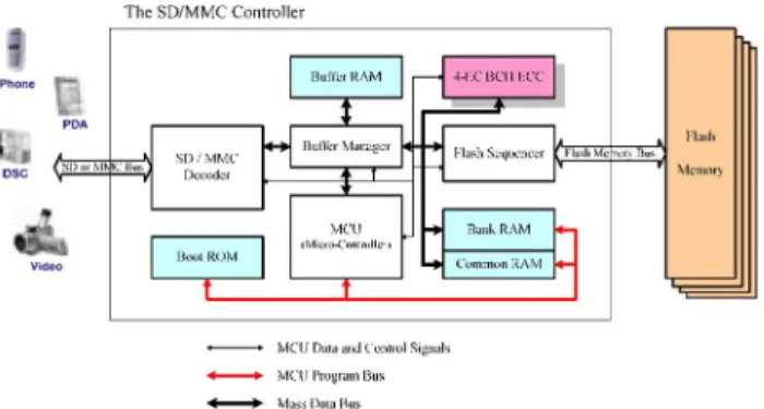
The functional block diagram of the NAND flash controller was shown in Fig. 1. The major functions of the controller can be divided as the -EC -bit parallel BCH ECC circuit, the code-banking structure, and firmware in-system programma-bility (ISP), the defect management and wear-leveling algo-rithm, and the dual channel and multi-buffering mechanism. The ECC circuit was designed here to enhance the data in-tegrity and reliability of the data stored in the flash memory. The code-banking structure for the microcontroller complying with firmware ISP function can provide the firmware upgrade to support various kind of flash memory. The defect management algorithm can increase the yield of the flash memory and pro-long the product life cycle by replacing the defected (bad) block with the reserved virgin (clean data) blocks. The wear-leveling algorithm was also introduced to prolong the product life cycle by preventing the flash memory blocks from unbalanced usage. The dual channel and multi-buffering mechanism was designed 0018-9464/$25.00 © 2007 IEEE
934 IEEE TRANSACTIONS ON MAGNETICS, VOL. 43, NO. 2, FEBRUARY 2007
Fig. 1. Block diagram of the NAND flash controller for SD/MMC card.
to increase the data transfer rate at the flash memory side and to fit the maximum bandwidth of the host–side interface bus. A. -EC BCH ECC Code Construction
For a typical -EC BCH code, the generator polynomial can be expressed as
(1)
where are the minimal polynomials
in GF(2 ).
By expanding the product of the left side of (1), the equation can be expressed as
(2) where ’s are coefficients of the generator polynomial
GF . In cyclic operation, can be implemented by a set of registers and XOR gates. Totally, registers are nec-essary to fulfill the cyclic operations. The (2) can be expressed as a matrix format as
(3) The detailed matrix form can be written as follows:
..
. ... ... . .. ...
..
. ... (4)
In serial connection, the matrix equation can be expressed as in (4). Moreover, for a continuously serial data input stream,
Fig. 2. w-bit folded structure for w-bit parallel operation.
, the -bit parallel for-mula can be formed as
.. .
By -times functional composition of the above equations, an analytical equation was deducted as follows:
(5) Based on the same concept and operations, the induction of the parallel syndrome polynomials is similar to the generator polynomials.
From the matrix operation of the (5), a general basic equation for the systolic array processing can be expressed as
(6) where the boundary conditions are
(7) (8) Based on the general basic equation of a -EC -bit parallel BCH code, the basic operation module for the matrix array can be constructed by two AND gates and two XOR gates. The co-efficients ’s are determined by the generator polynomial or the syndrome generator polynomials of the BCH code. To complete the matrix equation (4) by the basic operation module, an array
LIN AND DUNG: A NAND FLASH MEMORY CONTROLLER FOR SD/MMC FLASH MEMORY CARD 935
Fig. 3. Code-banking architecture.
Fig. 4. Micrograph of the controller chip.
architecture is adopted. The array architecture of the -bit input data stream for the BCH generator polynomial or syndrome gen-erator polynomials is shown as in Fig. 2.
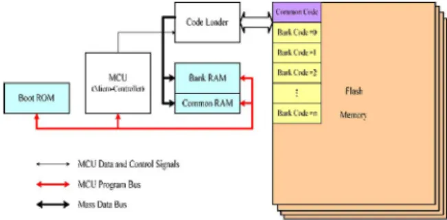
B. Code-Banking and Various NAND Flash Memory Support The architecture for the code-banking was shown in Fig. 3. The boot ROM was the masked read only memory, which stored the boot codes for the microcontroller in booting. By the code-banking architecture, the whole system firmware can be sepa-rated by several banks, Bank Code #0, 1, . The banked codes will be executed bank by bank when loaded by the code loader to the bank RAM. The system firmware of the microcon-troller can be upgraded from the host side.
To support the various kinds of the NAND flash memory in a controller, a specified flash parameter was created to record some system operated parameters of the NAND flash memory. The table was started by a start tag, and ended by an end-of-table flag. The useful parameters such as total capacity, total physical blocks, pages per block, etc. With the code-banking architecture and the specified flash memory parameters, the var-ious kinds of NAND flash memory can be supported in the same controller chip and be accessed in an optimal way respectively.
III. CHIPIMPLEMENTATION A. Controller Chip Implementation
The functional block diagram of the designed NAND flash controller for SD/MMC memory card was discussed in Sec-tion II (Fig. 1). With the chip architecture designed, the circuit of the chip was designed and implemented to the UMC 0.18 m CMOS Process. The chip micrograph of the designed NAND flash controller is shown in Fig. 4.
TABLE I
RESULTS OF THESYSTEMPERFORMANCE
B. Experiment and Test Results
The system performance of the designed NAND controller was evaluated by the certified platform of MMCA (http://www. mmca.org) and SDA (http://www.sdcard.org), the test platform was provided by Testmetrix, Inc. (http://www.testmetrix.com). The summary of the system performance of designed controller is shown in Table I.
IV. CONCLUSION
A NAND flash memory controller for SD/MMC memory card was presented. The -EC -bit parallel BCH ECC by using systolic array was presented, and it can be easily applied to a general -EC -bit parallel BCH ECC circuit application. The code-banking and ISP capability was presented and discussed for supporting the various kinds of the NAND flash memory. The real chip realization and the test results by experiment show the good performances of the controller chip.
REFERENCES
[1] P. Cappelletti, C. Golla, P. Olivo, and E. Zanoni, Flash Memories. Norwell, MA: Kluwer, 2000.
[2] D. R. Hankerson, D. G. Hoffman, D. A. Leonard, C. C. Lindner, K. T. Phelps, C. A. Rodger, and J. R. Wall, Coding Theory and
Cryptog-raphy. New York: Marcel Dekker, 2000.
[3] H. C. Chang, C. C. Lin, T. Y. Hsiao, J. T. Wu, and T. H. Wang, “Multi-level memory systems using error control codes,” Proc. Int. Symp.
Cir-cuits and Systems (ISCAS), pp. II 393–II 396, 2004.
[4] T. B. Pei and C. Zukowski, “High-speed parallel CRC circuits in VLSI,” IEEE Trans. Commun., vol. 40, no. 4, pp. 653–657, Apr. 1992. [5] X. Zhang and K. K. Parhi, “High-speed architectures for parallel long BCH encoders,” IEEE Trans. Very Large Scale Integr. (VLSI) Syst., vol. 12, no. 5, pp. 872–877, Jul. 2005.
[6] K. K. Parhi, “Eliminating the fan-out bottleneck in parallel long BCH encoders,” IEEE Trans. Circuits Syst., vol. 3, no. 51, pp. 512–516, 2004. [7] J. Zhang, Z. G. Wang, Q. S. Hu, and J. Xiao, “Optimized design for high-speed parallel BCH encoder,” in Proc. IEEE Int. Workshop VLSI
Design Video Tech., 2005, pp. 97–100.
[8] Y. Chen and K. K. Parhi, “Small area parallel chien search architectures for long BCH codes,” IEEE Trans. Very Large Scale Integr. (VLSI)
Syst., vol. 12, no. 5, pp. 545–549, May 2004.
[9] Y. Wu, “Low power decoding of BCH codes,” Proc. IEEE Int. Symp.
Circuits Systems (ISCAS), pp. II 369–II 372, 2004.
[10] K. Iwamura, Y. Dohi, and H. Imai, “A design of Reed–Solomon de-coder with systolic-array structure,” IEEE Trans. Comput., vol. 44, no. 1, pp. 118–122, Jan. 1995.