High-speed GaAs metal gate semiconductor field effect transistor structure grown on a
composite Ge Ge x Si 1 x Si substrate
Guang-Li Luo, Yen-Chang Hsieh, Edward Yi Chang, M. H. Pilkuhn, Chao-Hsin Chien, Tsung-Hsi Yang, Chao-Ching Cheng, and Chun-Yen Chang
Citation: Journal of Applied Physics 101, 084501 (2007); doi: 10.1063/1.2722245
View online: http://dx.doi.org/10.1063/1.2722245
View Table of Contents: http://scitation.aip.org/content/aip/journal/jap/101/8?ver=pdfcov Published by the AIP Publishing
Articles you may be interested in
Composition and strain in thin Si 1 x Ge x virtual substrates measured by micro-Raman spectroscopy and x-ray diffraction
J. Appl. Phys. 109, 033502 (2011); 10.1063/1.3536508
Control of semiconductor quantum dot nanostructures: Variants of Si x Ge 1 x / Si quantum dot molecules J. Vac. Sci. Technol. B 29, 011029 (2011); 10.1116/1.3533938
Temperature dependence of hole mobility in GaAs 1 x Bi x alloys J. Appl. Phys. 108, 083708 (2010); 10.1063/1.3493734
Electron tunneling in a strained n -type Si 1 x Ge x / Si / Si 1 x Ge x double-barrier structure Appl. Phys. Lett. 93, 123509 (2008); 10.1063/1.2991295
Effect of GaN cap layer grown at a low temperature on electrical characteristics of Al 0.25 Ga 0.75 N GaN heterojunction field-effect transistors
Appl. Phys. Lett. 85, 1430 (2004); 10.1063/1.1784038
High-speed GaAs metal gate semiconductor field effect transistor structure
grown on a composite Ge/ Ge
xSi
1−x/ Si substrate
Guang-Li Luoa兲
National Nano Device Laboratories, Hsinchu, Taiwan 30078, Republic of China
Yen-Chang Hsieh, Edward Yi Chang, and M. H. Pilkuhn
Department of Materials Science and Engineering, National Chiao Tung University, Hsinchu, Taiwan 30050, Republic of China
Chao-Hsin Chien, Tsung-Hsi Yang, Chao-Ching Cheng, and Chun-Yen Chang
Institute of Electronics, National Chiao Tung University, Hsinchu, Taiwan 30050, Republic of China
共Received 11 January 2007; accepted 28 February 2007; published online 17 April 2007兲
In this study we used a low-pressure metal organic vapor phase epitaxy method to investigate the growth of GaAs metal gate semiconductor field effect transistor 共MESFET兲 structures on a Si substrate. The buffer layer between the Si substrate and the grown GaAs epitaxial layers was a composite Ge/ Si0.05Ge0.95/ Si0.1Ge0.9metamorphic layer. We used transmission electron microscopy
to observe the microstructures formed in the grown GaAs/ Ge/ SixGe1−x/ Si material and atomic
force microscopy to analyze the surface morphology and the formation of antiphase domains in the GaAs epitaxial layers. The measured Hall electron mobility in the channel layer of a MESFET structure grown on a 6° misoriented Si substrate was 2015 cm2V−1s−1with a carrier concentration
of 5.0⫻1017cm−3. The MESFET device fabricated on this sample exhibited good current-voltage characteristics. © 2007 American Institute of Physics.关DOI:10.1063/1.2722245兴
I. INTRODUCTION
Heteroepitaxial growth of GaAs on Si substrates has at-tracted a great deal of attention in recent years because po-tentially it can be integrated into Si CMOS devices with the aid of high-k gate dielectrics1 to enhance performance and extend the roadmap. GaAs has a number of advantages over Si for some applications because of its higher electron mo-bility, wider band gap, and direct band gap. Nevertheless, silicon has several advantages over GaAs, including the abil-ity to fabricate devices over larger areas using mature pro-cesses and its higher thermal conductivity. The main prob-lems that must be overcome when growing GaAs on Si by heteroepitaxy are the large lattice mismatch 共4%兲 and the difference in the thermal expansion coefficients 共63%兲 of these two materials,2 which can cause high-density disloca-tions in the epitaxial GaAs layer. Several methods for reduc-ing the dislocation density have been reported, such as usreduc-ing strained layer superlattices共SLs兲 to confine dislocations and or using thermal cycle annealing to reduce threading dislocations.3 Motorola has reported a molecular beam epi-taxy共MBE兲-grown GaAs metal gate semiconductor field ef-fect transistor共MESFET兲 on Si using a SrTiO3buffer layer.
Unfortunately, it is difficult to grow the SrTiO3 buffer layer
in the MBE system.4
Germanium is only 0.07% lattice mismatched with GaAs, and the thermal expansion coefficient difference be-tween Ge and GaAs is only 2%, i.e., the lattice constant and thermal expansion coefficients of Ge are almost identical to those of GaAs. Although using a Ge layer as a buffer can solve the lattice mismatch problem between GaAs and Si,
the question arises as to how a high-quality Ge buffer layer can be grown on Si because Ge also has a 4.2% lattice mis-match with Si.
Many publications5,6 have described the growth of a pure Ge layer on a Si substrate using a graded SiGe buffer layer. The disadvantages are that the graded SiGe buffer layer must be sufficiently thick and that its surface must pos-sess a high degree of roughness and a crosshatched pattern. A method utilizing chemical-mechanical polishing 共CMP兲 was necessary to grow a relaxed graded SiGe buffer up to a 100% Ge layer.6
In a previous report, we proposed a simple Ge/SiGe buffer structure for the growth of high-quality GaAs layers on Si 共100兲 substrates.7 We demonstrated that such buffer structures are thin, have smooth surfaces, and exhibit a strong capability to block dislocations. This buffer growth technique has also been used by other authors for the fabri-cation of a high-performance Ge detector8 and for high-quality ZnSe heteroepitaxial growth on Si.9To prepare such a Ge/SiGe buffer structure 共see Fig. 1兲, a Si0.1Ge0.9layer is
first grown. Because of the large lattice mismatch between this layer and the Si substrate, many dislocations are inten-tionally generated in this first Si0.1Ge0.9 layer. A second
Si0.05Ge0.95 layer and a third Ge layer are subsequently
grown. The resulting Ge/ Si0.05Ge0.95/ Si01Ge09 and Si0.05Ge0.95 interfaces trap the upward-propagating disloca-tions very effectively; thereby, the dislocation density in the Ge layer is reduced significantly.
A common problem encountered at the GaAs/Ge inter-face is the formation of antiphase domains 共APDs兲, which occur when growing polar GaAs on nonpolar Ge. Several models have been reported for suppression of APDs through the use of Ge共100兲 wafers misoriented by 6° toward the
a兲Electronic mail: glluo@mail.ndl.org.tw
0021-8979/2007/101共8兲/084501/6/$23.00 101, 084501-1 © 2007 American Institute of Physics
⬍110⬎ direction.10,11
As growth proceeds, the initial nuclei grown only at the steps coalesce so that an APD-free GaAs is achieved. Another problem encountered during the growth of GaAs on Ge is the diffusion of Ge into the GaAs layer,12,13 which acts as an n-type dopant in GaAs.
In this study, a Ge/SiGe buffer was first grown through ultrahigh-vacuum chemical vapor deposition 共UHV/CVD兲. The sample was then transferred to another metal organic vapor phase epitaxy 共MOVPE兲 system to grow the GaAs MESFET structure. Herein, we describe this GaAs/Ge/ SiGe/Si heterostructure in detail.
II. EXPERIMENT
The growth of the SiGe and Ge buffer layers was under-taken using an UHV/CVD system operated at a base pressure below 2⫻10−8Torr. Disilane 共Si2H6兲 and germane 共GeH4兲
were used as source gases for Si and Ge, respectively. First, a 4-in. Si 共100兲 wafer with a 6° misorientation toward the 具110典 direction was subjected to a standard RCA cleaning and a 10 s dip in 10% HF solution and then went through a high-temperature共800 °C兲 baking in the growth chamber for 5 min. Next, 0.8m Si0.1Ge0.9, 0.8m Si0.05Ge0.95, and 1.0m Ge layers were grown sequentially at 400 °C. Be-tween successive layers, the growth was interrupted for in
situ annealing for 15 min at 750 °C. Here, we did not grow
Si buffer layer before Si0.1Ge0.9growth, because we did not
find any difference. After the growth of this Ge/SiGe/Si metamorphic structure was complete, the sample was loaded out and immediately transferred to a LP-MOVPE system for growth of GaAs at 630 °C under a reactor pressure of 40 Torr. The sources of Ga and As were triethylgallium共TEGa兲 and AsH3, respectively. Diluted SiH4 in H2 was used as an
n-type dopant. The investigations in this study were
three-fold. The first involved the formation of antiphase bound-aries at different growth temperatures. For comparison, we attempted to grow GaAs buffer layers at different tempera-tures on Ge/SiGe/Si structempera-tures by using 0°-misoriented Si共100兲 substrates. In this case, GaAs buffer layers each hav-ing a thickness of 0.1m were grown at 450, 500, and 550 °C, respectively. Following the growth of each GaAs buffer layer, an undoped GaAs layer having a thickness of ⬃2.2m was grown at 630 °C. In our second investigation, we grew the same structures on Si共100兲 substrates with a 6° misorientation toward the具110典 direction. This study focused on suppression of the antiphase boundaries using misoriented substrates. Finally, based on the material structure that was grown on a 6° misoriented Si substrate, GaAs MESFET de-vices having a gate length of 0.5m and a width of 100m were fabricated using standard III-V MESFET processing techniques. The source-drain ohmic contacts were AuGe/ Ni/Au formed by rapid thermal annealing, while the gate metallization was TiPtAu. Throughout this study, transmis-sion electron microscopy 共TEM兲 was used to measure the thickness of the epitaxial layers and observe the dislocation distribution; double-crystal x-ray diffraction 共DCXRD兲 was used to analyze the crystalline quality.
III. RESULTS AND DISCUSSION
A. Effect of low-temperature GaAs buffers on size of APDs
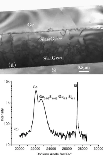
Figure2共a兲displays a cross-sectional TEM image of the Ge buffer layers grown on the Si substrate. The total thick-ness of the epitaxial structure was only⬃2.6m. It can be found there were a large number of dislocations located in the Si0.1Ge0.9layer near the Si0.1Ge0.9/ Si interface due to the
large Ge composition difference between Si0.1Ge0.9 and Si.
The upward-propagated dislocations were bent sideways and terminated very effectively by the Si0.05Ge0.95/ Si0.1Ge0.9and
Ge/ Si0.05Ge0.95interfaces because of the compressive stress
induced at the interfaces. Very few threading dislocations FIG. 2. 共a兲 Cross-sectional TEM image and 共b兲 x-ray rocking curve of
stacked Ge and SiGe epilayers on a Si substrate.
FIG. 1. Schematic illustration of a GaAs MESFET fabricated on a Si substrate.
084501-2 Luo et al. J. Appl. Phys. 101, 084501共2007兲
could propagate into the top Ge layer. Details of the growth of the Ge/SiGe buffer layers can be found elsewhere.7Figure
2共b兲displays the rocking curve of the stacked Ge and SiGe epilayers. The intense and sharp Ge peak indicates that the grown top Ge layer was of a very high crystalline quality.
A LP-MOVPE system was used to grow GaAs layers on the above-mentioned composite Ge/SiGe/Si substrates. Al-though the low lattice mismatch of the GaAs/Ge system sug-gests that it should be almost dislocation-free, considerable problems remained during the epitaxy between the polar 共GaAs兲 on nonpolar 共Ge兲 semiconductors, resulting in the formation of antiphase domains 共APDs兲. On 共100兲 surfaces, the atoms nucleate at both steps and terraces with the latter having a crystal orientation that is rotated by 90°; the phase 共or domain兲 polarity depends on the growth temperature and the substrate misorientation angle.10 At the boundary be-tween two APDs, an antiphase boundary 共APB兲 is created. The APB consists of wrong bonds of As–As or Ga–Ga,
which can provide deep levels in the forbidden gap and act as nonradiative recombination centers. We attempted to sup-press APBs by growing low-temperature GaAs buffer layers on the Ge surfaces with Si substrates having a 0° misorien-tation. Unfortunately, we could not control the adatoms to nucleate only at steps or terraces; i.e., the GaAs layer could not be grown in only one domain. Figure 3共a兲presents the surface morphology of the GaAs layer grown on the 0°-misoriented substrate at 550 °C. Two domains are clearly evident. The winding dark lines between two antiphase do-mains are antiphase boundaries. Taken together with Figs.
3共b兲 and 3共c兲, we observed that the sizes of the APDs in-creased upon increasing the growth temperature of the GaAs buffer layer, possibly because a higher temperature increased the diffusion length of the surface species. At a low growth temperature, the mobility of the atoms was kinetically de-layed, such that atoms could only diffuse a short distance before they became incorporated. As a result, we observe high-density APDs of a smaller size in Fig.3共c兲. As a con-sequence of the formation of APBs, the surface of each sample was very rough. For the sample for which the GaAs buffer layer was grown at 550 °C, the surface root mean square 共rms兲 roughness was 70.35 Å and the roughness av-erage 共Ra兲 was 60.61 Å.
B. Suppression of APBs using misoriented Si substrates
The low-temperature GaAs buffer could not sufficiently suppress the APBs. The most common method for avoiding the formation of APDs at GaAs/Ge interfaces is the use of misoriented substrates and a sufficient amount of thermal annealing. The suppression of APDs can be achieved by us-ing a Si wafer with a misorientation angle. For substrates having a larger misorientation angle 共艌6°兲, in which the terraces between the steps are very narrow, the steps are so close to each other that the nuclei can be formed only at the steps, with a diminished possibility for two-dimensional FIG. 3.共Color online兲 AFM images of GaAs layers grown on the composite
Ge/ SixGe1−x/ Si substrate共the Si substrate was 0° misoriented兲 with
differ-ent low temperature GaAs buffers共a兲 550, 共b兲 500, and 共c兲 450 °C. Scanned area: 25⫻25m.
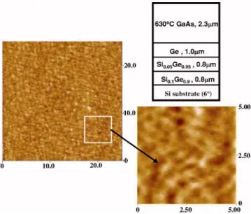
FIG. 4. 共Color online兲 AFM image and layer structures of GaAs grown on the composite Ge/ SixGe1−x/ Si substrate at 630 °C共the Si substrate was 6°
misoriented兲. Scanning area: 25⫻25m.
nucleation on the terraces. As the growth proceeds, the initial nuclei that formed at the steps coalesce so that only one domain of GaAs is achieved; other domains associated with nucleation on terraces are avoided. Consequently, a blanket GaAs layer with a single sublattice orientation共or phase兲 can be grown on a艌6° misoriented 共100兲 surface. In this study, we grew the sample on a Ge/SiGe/Si substrate at a 6° mis-orientation angle. Here, the growth temperature was 630 °C; no low-temperature GaAs buffer was employed. The atomic force microscopy 共AFM兲 image in Fig. 4 indicates that no APDs existed on the surface. The measured rms roughness was only 7.35 Å and the value of Ra was only 5.81 Å. We
believe that the reason for this smoothness was the suppres-sion of APBs on the misoriented共100兲 surface.
We used secondary ion mass spectrometry共SIMS兲 tech-niques to verify the interdiffusion of the Ge layer into GaAs. This technique provides quantitative measurements of the levels of dopants and impurities in semiconductors. As men-tioned above, the formation of APBs depended primarily on the magnitude of the misorientation angle of the Si 共100兲 substrate. Figures5共a兲–5共c兲display the depth profiles for Ge diffusion into the GaAs layer. We observed different lengths of Ge diffusion into the GaAs layer according to the various misorientation angles of the Si substrate. Figure 5共a兲 indi-cates that the Ge diffused by⬃0.75m into the GaAs layer when the substrate was misoriented by 0°. When the degree of substrate misorientation was greater than 6°, the Ge dif-fusion into the GaAs layer was only ⬃0.25m 关see Fig. FIG. 5.共Color online兲 Layer structures, SIMS profiles, and AFM images for the GaAs layers grown on the Ge/SixGe1−x/ Si substrates at misorientation angles
of共a1–a3兲 0°, 共b1–b3兲 4°, and 共c1–c3兲 6°.
084501-4 Luo et al. J. Appl. Phys. 101, 084501共2007兲
5共c兲兴. Here, the APBs may be considered as routes for Ge diffusion into the GaAs layer during the growth process. The lowest degree of Ge diffusion into GaAs in Fig.5共c兲may be due to the total suppression of the formation of APDs. Figure
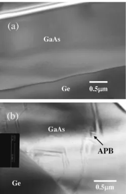
6共a兲displays the GaAs layer grown on the 6° misoriented Si substrate; no twins or lattice defects appear around the GaAs/Ge interface. Figure 6共b兲 presents the GaAs layer grown on the 0° misoriented Si substrate ; we observed APBs penetrating through the GaAs layer from the Ge layer. These results suggest that a relationship exists between the degree of Ge diffusion and the formation of APBs.
C. Material characterization and MESFET devices
MESFET devices were fabricated on the material struc-ture displayed in Fig.6共a兲. In this sample, the total thickness of GaAs was 2.3m µm, on top of which were grown a 1500 Å thick channel 共Si doped at 5.0⫻1017cm−3兲 and a
500 Å contact layer 共Si doped at 5⫻1018cm−3兲. A
double-crystal x-ray measurement of the sample displays five peaks in the diffraction spectrum; i.e., for GaAs, pure Ge, Si0.1Ge0.9, Si0.05Ge0.95, and the Si substrate共Fig.7兲. The full
width at half maximum共FWHM兲 for the GaAs peak was 120 arcsec. By using the common formula N =共⌬/ b兲2关where N is the dislocation density, ⌬ is the FWHW, and b is the Burgers vector 共0.4 nm兲兴,14–16 we roughly estimate the dis-location density in GaAs to be 6.0⫻106cm−2. We also did
the etch pits test by using KOH etching; the pit density is about 7⫻106/ cm2, which is of the same order as the value of
XRD measurement. A Hall measurement was performed on the GaAs/Ge/SiGe structure at room temperature using the van der Pauw method. The measured electron mobility was 2015 cm2V−1s−1 with a carrier concentration of 5.0 ⫻1017cm−3. Figure 8共a兲 displays the drain current-voltage
共I-V兲 characteristics for the MESFET device; the good pinch-off behavior indicates the good crystallinity of the GaAs layer grown on the Si substrate. The saturation current is 142 mA/mm at gate voltage VG= 0 V. The transfer
char-acteristic of Fig.8共b兲displays a maximum transconductance of 150 mS/mm at drain-source voltage VDS= 1.5 V. These
results suggest that the material structure grown in this work is very promising for the fabrication of Si-based GaAs chan-nel high-speed electronic devices.
FIG. 6. TEM images of GaAs grown on composite Ge/SiGe/Si substrates at Si substrate misorientation angles of共a兲 6° and 共b兲 0°.
FIG. 7. Double-crystal x-ray diffraction spectrum of a GaAs layer grown on a composite Ge/ SixGe1−x/ Si substrate.
FIG. 8. 共Color online兲 共a兲 Drain I-V characteristics and 共b兲 transfer charac-teristics of a fabricated 0.5⫻100m2 MESFET device based on GaAs
grown on a composite Ge/ SixGe1−x/ Si substrate at a 6° misorientation.
IV. CONCLUSIONS
A Ge/ Si0.05Ge0.95/ Si0.1Ge0.9buffer layer was used to ac-commodate the strain induced between a Si substrate and a GaAs layer and to prevent threading dislocations from pen-etrating into the top GaAs layers. A misoriented substrate 共艌6°兲 was employed to suppress APB formation in the GaAs layer. We found that the sizes of the APDs depended upon growth temperature of the GaAs buffer layers. The Hall elec-tron mobility of the GaAs channel layer grown on the Ge/ SixSi1−x/ Si structure was 2015 cm2V−1s−1with a carrier
concentration of 5.0⫻1017cm−3. A GaAs MESFET device
fabricated on this material exhibited good dc characteristics.
1R. Droopad, M. Passlack, N. England, K. Rajagopalan, J. Abrokwah, and
A. Kummel, Microelectron. Eng. 80, 138共2005兲.
2K. S. Kim, J.-H. Kim, D. H. Lim, G. M. Yang, J. Y. Kim, and H. J. Lee,
J. Cryst. Growth 179, 427共1997兲.
3N. Y. Jin-Phillipp, F. Phillipp, T. Marschner, W. Stolz, and E. O. Gobel, J.
Cryst. Growth 158, 28共1996兲.
4K. Eisenbeiser, R. Emrick, R. Droopad, Z. Yu, J. Finder, S. Rockwell, J.
Holmes, C. Overgaard, and W. Ooms, IEEE Electron Device Lett. 23, 300 共2002兲.
5S. B. Samavedam and E. A. Fitzgerald, J. Appl. Phys. 81, 3108共1997兲. 6M. T. Currie, S. B. Samavedam, T. A. Langdo, C. W. Leitz, and E. A.
Fitzgerald, Appl. Phys. Lett. 72, 1718共1998兲.
7G. L. Luo, T.-H. Yang, E. Y. Chang, C.-Y. Chang, and K.-A. Chao, Jpn. J.
Appl. Phys., Part 2 42, L517共2003兲.
8Z. H. Huang, J. Oh, and J. C. Campbell, Appl. Phys. Lett. 85, 3286共2004兲. 9J. T. Ku, M. C. Kuo, J. L. Shen, K. C. Chiu, T. H. Yang, G. L. Luo, C. Y.
Chang, Y. C. Lin, C. P. Fu, D. S. Chuu, C. H. Chia, and W. C. Chou, J. Appl. Phys. 99, 063506共2006兲.
10L. Lazzarini, L. Nasi, G. Salviati, C. Z. Fregonara, Y. Li, L. J. Giling, and
D. B. Holt, Micron 31, 217共2000兲.
11Y. Li, G. Salviati, M. M. G. Bongers, L. Lazzarini, L. Nasi, and L. J.
Giling, J. Cryst. Growth 163, 195共1996兲.
12W. Li, S. Laaksonen, J. Haapamaa, and M. Pessa, J. Cryst. Growth 227– 228, 104共2001兲.
13P. Modak, M. K. Hudait, S. Hardikar, and S. B. Krupanidhi, J. Cryst.
Growth 193, 501共1998兲.
14P. Gay, P. B. Hirsh, and A. Kelly, Acta Metall. 1, 315共1953兲.
15R. D. Dupuis, J. C. Bean, J. M. Brown, A. T. Macrander, R. C. Miller, and
L. C. Hopkins, J. Electron. Mater. 16, 69共1987兲.
16L. Tapfer, J. R. Martinez, and K. Ploog, Semicond. Sci. Technol. 4, 617
共1989兲.
084501-6 Luo et al. J. Appl. Phys. 101, 084501共2007兲