ECS Journal of Solid State Science and Technology, 1 (2) Q35-Q37 (2012) Q35 2162-8769/2012/1(2)/Q35/3/$28.00©The Electrochemical Society
Investigation of GaN Films Grown on Liquid-Phase Deposited SiO
2Nanopatterned Sapphire Substrates
Cheng-Yu Hsieh, Bo-Wen Lin, Hsin-Ju Cho, Bau-Ming Wang, and YewChung Sermon Wu*,z
Department of Materials Science and Engineering, National Chiao Tung University, Hsinchu 300, Taiwan
A simple, easy and relatively inexpensive liquid phase deposition (LPD) method was used to introduce nano SiO2on sapphire substrates to fabricate nanoscale patterned sapphire substrates (PSS). Two kinds of nanoscale PSS were used to grow GaN, namely “NPOS” which is nano-pattern oxide on sapphire substrate and “NPSS” which is nano-patterned sapphire substrate. It was found that upper region of NPSS-GaN had the best quality. This is because as the growth time increased, laterally-grown GaN caused the threading dislocations to bend toward the patterns. Besides, voids formed on the NPSS pattern sidewalls caused more threading dislocation bending toward these voids.
© 2012 The Electrochemical Society. [DOI:10.1149/2.007202jss] All rights reserved.
Manuscript submitted February 15, 2012; revised manuscript received April 17, 2012. Published July 20, 2012.
High-brightness GaN-based light-emitting diodes (LEDs) have been highly demanded in various fields. For the purpose of next-generation application of solid-state lighting, LEDs with higher in-ternal and exin-ternal quantum efficiency are required. Among many methods, lots of efforts have been invested on patterned sapphire sub-strates (PSS) to improve the quality of GaN film and light extraction efficiency.1–3
In PSS, microscale patterned substrates with grooves, pyramids or other patterns are usually fabricated by dry or wet etching process. As the growth time increased, GaN epilayers on the c-plane sapphire covered these patterns by lateral growth causing the threading disloca-tion to bend toward the microscale patterns. Therefore, the threading dislocation densities on the upper regions were reduced.1As a result, the internal quantum efficiency and the leakage current of GaN-based LEDs were improved.4–6
If the lateral overgrowth approach is reduced to the nanoscale, the-oretical and experimental studies indicate that a further reduction in the defect density is possible.7Several technologies have been applied to fabricate nanoscale PSS like nanoimprint lithography, nanosphere lithography and forming nanorods by using self-assembled Ni as etch-ing mask.8–12In this study, liquid phase deposition (LPD) was used to introduce nanoscale SiO2hemispheres on sapphire substrates to
fabri-cate nanoscale PSS’s.12–15Compared to other nanoscale PSS process, the LPD-SiO2process was simpler, easier and relatively inexpensive.
With these nanoscale patterns, the crystal quality and optical perfor-mance of GaN were improved.
Experimental
Two kinds of nanoscale PSS were used to grow GaN. Samples designated as “NPOS” are nano-pattern oxide on sapphire substrate, while samples designated as “NPSS” are nano-patterned sapphire sub-strate. Two-inch c-plane sapphire substrate was used in this study. LPD was used to fabricate NPOS. Sapphire substrate was first immersed in mixed solution of H2SiF6 saturated with silica gel and H3BO3
(0.01 mol/l) for 60 min. The related LPD reaction equations on sap-phire substrate were listed as follows:
H3B O3+ 4HF ↔ BF4−+ H3O++ 2H2O (1) H2Si F6+ 2H2O↔ 6H F + Si O2 (2)
SiO2 can be formed after the dehydration of OH-bonded
silox-ane oligomer [SiFm(OH)4−m] by catalytic reaction.12These substrates
were then annealed at 900◦C in N2ambient for 30 minutes to improve
SiO2quality.
To fabricate the NPSS, NPOS was etched in hot H3PO4–based
so-lutions. Then, samples were dipped into 1% diluted hydrogen fluoride (DHF) solution to remove the LPD- SiO2.16
*Electrochemical Society Active Member. zE-mail:[email protected]
After the cleaning process, GaN-based LED structures were grown by metal-organic chemical vapor deposition (MOCVD) on both sub-strates. For the purpose of comparison, LED structures were also grown on unpatterned sapphire substrate and denoted as FLAT. The crystal quality and optical performance of GaN were characterized by atomic force microscopy (AFM), scanning electron microscopy (SEM), transmission electron-microscopy (TEM), X-ray diffraction (XRD), monochromated cathodoluminescence (CL) and photolumi-nescence (PL).
Results and Discussion
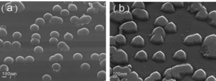
Figure1presents the SEM images of NPOS and NPSS. The shape of LPD-SiO2patterns on the surface of sapphire was hemisphere with
200–300 nm in diameter and 100–150 nm in height (measured by AFM). As shown in Figs.1a, these SiO2hemispheres were randomly
distributed on the sapphire surface. The structure of NPSS pattern comprised a triangle pyramid covered with a flat top (0001) c-plane. The diameter of pyramids was about 250–300 nm, and the height was 140–170 nm.
The nature of GaN crystal qualities on sapphire substrates was first analyzed by XRD rocking curves. Both symmetric (002) and asymmetric (102) reflections were measured as shown in TableI. The full width at half maximum (FWHM) values of NPSS-GaN were less than those of NPOS-GaN and FLAT-GaN. These results indicate that the GaN crystallinity of NPSS-GaN is superior to that of NPOS-GaN and FLAT-GaN.
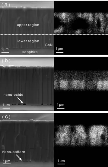
Figure 2 is cross section SEM images and corresponding monochromated CL maps taken at wavelengths of 370 nm, respec-tively. Clearly, the upper region of the GaN film exhibited bright contrast in the CL maps which correspond to strong excitation with much less non-radiative centers in this region. In contrast, the lower region appeared dark contrast, implying that it is highly defected. Be-sides, Fig.2also shows that the CL contrast of the upper regions of NPSS-GaN and NPOS-GaN was brighter than that of FLAT-GaN.
The CL spectra intensities collected around the lower and upper regions are summarized in Table I. At the lower regions, the inte-gral intensities of NPSS-GaN and NPOS-GaN were about the same
Figure 1. SEM images of (a) NPOS and (b) NPSS.
) unless CC License in place (see abstract).
ecsdl.org/site/terms_use
address. Redistribution subject to ECS terms of use (see
140.113.38.11
Q36 ECS Journal of Solid State Science and Technology, 1 (2) Q35-Q37 (2012)
Table I. Characteristics of GaN grown on sapphire.
FWHM of XRCs (arcsec) Integral CL spectrum
(002) (102) EPD (cm−2) lower region upper region
FLAT-GaN 427.9 586.9 3.3× 10⁷ 2.9× 10⁴ 3× 10⁵
NPOS-GaN 389.2 522.9 8× 10⁶ 9.3× 10⁴ 1.5× 10⁶
NPSS-GaN 362.4 390.1 3.9× 10⁶ 9.1× 10⁴ 1.9× 10⁶
(∼9 × 10⁴), which was 3 times higher than that of FLAT-GaN. At
the upper regions, the integral intensity of NPSS-GaN was 1.9× 10⁶,
which was 1.27 times higher than that of NPOS-GaN, and 6.33 times higher than that of the FLAT-GaN.
The improvement on structural quality at the upper region was verified by measuring etch pit density (EPD). All three samples were grinded till undoped-GaN revealed (∼2.5 μm from the GaN/sapphire interface). Then, the samples were etched in 270◦C H3PO4for 3 min.
As listed in TableI, the EPD of NPSS-GaN was 3.9× 106 cm−2,
which was 48.75% of NPOS-GaN, and 11.82% of FLAT-GaN. In other words, NPSS-GaN did have the best crystal quality at the upper region.
TEM was also used to investigate the crystal qualities in both regions. As shown in Fig.3a, many dislocations were observed at the lower region. They originated from the GaN/sapphire interface due
Figure 2. SEM images and corresponding monochromated CL maps of (a) FLAT-GaN, (b) NPOS -GaN and (c) NPSS -GaN.
to the large lattice misfit. Many of them then extended to the upper region. As for the NPSS-GaN and NPOS-GaN (Figs.3band3c), as the growth time increased, GaN epilayers on the c-plane sapphire covered these nano patterns by lateral growth causing the threading dislocation to bend toward the patterns. Therefore, the dislocation densities on the upper regions were reduced.
These TEM observations clearly explain the CL observations. That the upper regions of the GaN film exhibited bright CL contrasts is because these regions had low defect/dislocation densities. Besides, that the CL contrast of the upper regions of NPSS-GaN and NPOS-GaN was brighter than that of FLAT-NPOS-GaN is because their threading dislocation bended toward the nano patterns at the lower regions. As a result, their upper regions had low defect densities.
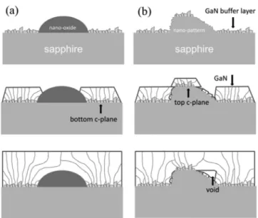
Figures3band3calso reveal that NPSS-GaN patterns had more bending dislocations than NPOS-GaN at the lower regions. This might be because the GaN growth mechanism on NPSS was different from that on NPOS. As illustrated in Fig.4a, most of the growth of GaN on NPOS was initiated from bottom c-planes. As the growth time increased, lateral growth GaN epilayers caused the threading disloca-tions to bend toward the patterns, as mentioned previously.1
As illustrated in Fig.4d, GaN initiates not only from bottom c-planes, but also from top c-planes for the growth of NPSS-GaN. It is evident that as the growth time increased, the two growth fronts collided to each other. As a result, some voids (∼50 nm in size) were left on the pattern sidewall, as shown in Figs.3cand4b. These voids were associated with the relaxed morphologies of the GaN film side faces and caused more threading dislocation to bend toward these voids. Consequently, the threading dislocation density was effectively reduced.17
PL was used to investigate the quality of muti-quantum wells. The excitation source was a 325 nm, 30 mW He–Cd continuous wave laser. As Fig.5shows, the PL peak intensity of MQWs grown on NPSS is 1.2 times higher than that on NPOS, and 1.5 times higher than that on FLAT. This observation suggests that nano patterns in NPSS can efficiently improve MQWs quality via improving crystal quality at the upper region (through bending threading dislocations toward the patterns at the lower regions).
Figure 3. Cross-section TEM images of GaN grown on (a) FLAT sapphire, (b) NPOS, and (c) NPOS. The black dots in image are Ga drops formed from FIB ion milling.
) unless CC License in place (see abstract).
ecsdl.org/site/terms_use
address. Redistribution subject to ECS terms of use (see
140.113.38.11
ECS Journal of Solid State Science and Technology, 1 (2) Q35-Q37 (2012) Q37
Figure 4. Schematic diagrams of evolution of GaN grown on (a) NPOS and (b) NPOS.
Figure 5. The photoluminescence of muti-quantum-wells grown on FLAT sapphire, NPOS and NPSS.
Conclusions
High quality SiO2 hemispheres and sapphire nano-patterns are
fabricated on sapphire substrate by combining LPD method and wet etch process. The GaN films have fully coalesced and the voids can only be found in the case of GaN grown on NPSS. The XRCs, EPD and monochromated CL maps show that the GaN grown on PSSs has better quality than on FLAT sapphire. Moreover, the integral CL spectra show that the GaN grown on NPSS has relatively lower defect density than on NPOS and FLAT sapphire. TEM analysis reveal that parts of dislocation in the GaN grown on NPSS bend to voids and hence largely lower the defect density. The MQWs grown on NPOS and NPSS indicate 1.2 and 1.5 times enhancement in PL intensity than that in FLAT sapphire.
Acknowledgments
This project was funded by Sino American Silicon Products Incor-poration and the National Science Council of the Republic of China under grant No. 98-2221-E009-041-MY3. Technical supports from the National Nano Device Laboratory, Center for Nano Science and Technology, Nano Facility Center and Semiconductor Laser Tech-nology Laboratory of the National Chiao Tung University are also acknowledged.
References
1. J. H. Cheng, Y. C. Sermon Wu, W. C. Liao, and B. W. Lin,Appl. Phys. Lett., 96, 051109 (2010).
2. B. W. Lin, C. Y. Hsieh, B. M. Wang, W. C. Hsu, and Y. C. Sermon Wu,Electrochem. Solid-State Lett., 14, 48 (2011).
3. B. W. Lin, C. C. Chang, C. Y. Hsieh, B. M. Wang, Y. C. Sermon Wu, and W. C. Hsu, IEEE Photon. Tech. Lett., 23, 1772 (2011).
4. I. Lo, K. Y. Hsieh, S. L. Hwang, and L. W. Tu,Appl. Phys. Lett., 74, 2167 (1999). 5. P. Kozodoy, J. P. Ibbetson, H. Marchand, P. T. Fini, S. Keller, J. S. Speck,
S. P. DenBaars, and U. K. Mishra,Appl. Phys. Lett., 73, 17 (1998).
6. K. Tadatomo, H. Okagawa, Y. Ohuchi, T. Tsunekawa, Y. Imada, M. KaTo, and T. Taguchi,Jpn. J. Appl. Phys., 40, L583 (2001).
7. H. Gao, F. Yan, Y. Zhang, J. Li, Y. Zeng, and G. Wang,J. Appl. Phys., 103, 014314 (2008).
8. S. Y. Chou, P. R. Krauss, and P. J. Renstrom,J. Vac. Sci. Technol. B, 14, 4129 (1996). 9. H. W. Huang, C. H. Lin, J. K. Huang, K. Y. Lee, C. F. Lin, C. C. Yu, J. Y. Tsai,
R. Hsueh, H. C. Kuo, and S. C. Wang,Mater. Sci. Eng. B, 164, 76 (2009). 10. C. H. Chiu, H. H. Yen, C. L. Chao, Z. Y. Li, and P. Yu,Appl. Phys. Lett., 93, 081108
(2008).
11. J. J. Chen, Y. K. Su, C. L. Lin, S. M. Chen, W. L. Li, and C. C. Kao,IEEE Photon. Tech. Lett., 20, 1193 (2008).
12. C. H. Chan, C. H. Hou, S. Z. Tseng, T. J. Chen, and H. T. Chien,Appl. Phys. Lett., 95, 011110 (2009).
13. H. Nagayama, H. Honda, and H. Kawahara,J. Electrochem. Soc., 138, 2013 (1988). 14. M. C. Hsu, Y. M. Sun, I. C. Leu, and M. H. Hon,J. Electrochem. Soc., 153, F260
(2006).
15. M. K. Lee, C. L. Ho, and C. H. Fan,Appl. Phys. Lett., 92, 061103 (2008). 16. F. Dwikusuma, D. Saulys, and T. F. Kuech,J. Electrochem. Soc., 149, G603 (2002). 17. W. K. Wang, D. S. Wuu, W. C. Shih, J. S. Fang, W. Y. Lin, P. Han, R. H. Horng, T. C. Hsu, T. C. Huo, M. J. Jou, A. Lin, and Y. H. Yu,Jpn. J. Appl. Phys., 44, 2512 (2005).
) unless CC License in place (see abstract).
ecsdl.org/site/terms_use
address. Redistribution subject to ECS terms of use (see
140.113.38.11