Effect of Annealing on the Microstructure and Electrical
Property of RuN Thin Films
Chia-Yang Wu,aWen-Hsi Lee,aShih-Chieh Chang,bYi-Lung Cheng,cand Ying-Lang Wangb,z
a
Department of Electrical Engineering, National Cheng Kung University, Tainan 701, Taiwan b
Institute of Lighting and Energy Photonics, National Chiao Tung University, Hsinchu 30050, Taiwan c
Department of Electrical Engineering, National Chi-Nan University, Nan-Tou, Taiwan
Ruthenium共Ru兲 and ruthenium nitride 共RuN兲 thin films have been investigated as candidates for barrier layers in copper 共Cu兲 damascene processes. In order to study the thermal stability of the Ru and RuN films, the as-deposited films were annealed by rapid thermal annealing共RTA兲, and the film resistance was real-time measured by a four-point probe, which was embedded in the RTA tool. The X-ray diffraction data show that the grain size of Ru decreased with the increase of the nitrogen共N兲 content. The Ru phases gradually changed to the RuN phases, and the resistivity of the RuN films decreased with annealing time due to nitrogen effusion. Discontinuous RuN films were found when the annealing temperature was higher than 800°C and then caused a poor Cu diffusion barrier property. We also demonstrated that the Cu film could be directly electroplated on the RuN films with adequate adhesion.
© 2011 The Electrochemical Society. 关DOI: 10.1149/1.3537825兴 All rights reserved.
Manuscript submitted June 21, 2010; revised manuscript received November 22, 2010. Published January 25, 2011.
As the minimum feature size of microelectronic devices shrinks down to 32 nm and beyond, an increase in the resistivity of metal lines with feature shrinkage will be one of the semiconductor manu-facturing challenges. In recent years, ruthenium共Ru兲 metal has been investigated as a barrier material for copper共Cu兲 metallization be-cause 共i兲 it facilitates direct electroplating of Cu without a seed layer;共ii兲 its adhesion to Cu is good even in the absence of a Cu seed layer; and共iii兲 its solubility in Cu is low, and thus its impurity effect on Cu resistivity will be minimal.1-17However, for pure Ru, it has been found that its barrier property for Cu diffusion is worse than that of tantalum and tantalum nitride共Ta/TaN兲 and Cu diffu-sion occurs after annealing at 450°C for 10 min in a Cu/Ru/Si structure.1-4Therefore, how to modify the Ru metal as a Cu plate-able diffusion barrier layer is very important for Ru to replace Ta/TaN. Several reports found that the ruthenium nitride 共RuN兲 bar-rier has a better thermal stability than that of the pure Ru.5-8 Dam-ayanti et al.9reported that these advantages can be attributed to the dissolved nitrogen 共N兲 atoms in the amorphous films and the N atoms stuffed in the grain boundaries in the crystalline films, and the same report also clarified the peak of RuN phase on the X-ray dif-fraction共XRD兲 spectra.9Ogawa et al.10reported that the N atmo-spheres would only change the Ru into the amorphous type. In the same article, the stacked barrier structure 共amorphous Ru/ polycrystalline Ru兲 was proposed as a highly reliable barrier metal structure. In this study, we prepared RuN films with various N con-tents to investigate their barrier property and thermal stability. Fur-thermore, the phase transformation, the agglomeration behavior, the antidiffusion property, and the behavior of copper electroplating on various RuN films were studied by in situ sheet resistance 共Rs兲 measurement, XRD, atomic force microscopy 共AFM兲, scanning electron microscope共SEM兲, and X-ray photoelectron spectroscopy 共XPS兲. Consequently, we may determine N content of the RuN films to optimize the barrier properties.
Experimental
A p-Si共111兲 wafer was chosen as the substrate for this study. The Ru layer 共99.99% purity兲 was sputtered onto Si wafers at room temperature in a direct-current magnetron-sputtering machine. The base pressure and working pressure were controlled at 10−6Torr and
⬃5 mTorr, respectively. Before sputtering, the sample was degassed at 300°C for 60 s. Deposition was carried out in nitrogen共N2兲 and
argon共Ar兲 atmosphere with different N2flow rates. The thickness of the Ru and RuN films was controlled at 20 nm, and then a 50-nm
thick Cu共99.99% purity兲 layer was subsequently sputtered onto the samples at room temperature with a 5 mTorr working pressure.
Rapid thermal annealing 共RTA兲 was applied to anneal the RuN/Si and Cu/RuN/Si for 5 min and 1 h, respectively. The anneal-ing temperature was chosen between 100 and 800°C in N2 and
hydrogen共H2兲 atmospheres. The texture was analyzed by XRD
us-ing a Bruker D8 SSS multipurpose thin-film X-ray diffractometer with 1.542 Å共Cu K␣兲 incident rays. The electron binding energy of Ru and the stoichiometric composition of the RuN films were mea-sured by XPS. The films thickness and cross-sectional images were examined with HITACHI S-4800 SEM, while the surface roughness was measured using a NT-MDT P47E10 P7LS AFM. The sheet resistance was measured with a 280SI four-point probe.
A high-purity Cu sulfate共CuSO4·5H2O, Aldrich兲 was dissolved in deionized water and sulfuric acid共H2SO4, Mallinckrodt兲 to make
electrolytes for Cu electroplating. The electrochemical experiments were performed using an Autolab PGSTA302N. A conventional three-electrode cell with a Pt sheet as the counter electrode and Ag/AgCl 共3 M KCl兲 as the reference electrode was employed. After Cu electroplating, 3M Scotch packing tapes were used to roughly check the adhesion between the Cu films and the Ru or RuN films.2-4,15
Results and Discussion
RuN/Si structure.— The different RuN samples were prepared
with six different N2flow ratios共N2/N2+ Ar兲 that were from 0 to
56%. The resistivity and deposition rate of the Ru and RuN films are shown in Fig.1a, which reveals that the film resistivity increased and the deposition rate decreased with the rise in the N2flow ratio.
In this study, the resistivity of the RuN films was smaller than 80⍀ cm, which was smaller than 150–200 ⍀ cm of typical TaN films. The more N2gas in the reaction, the more Ru-N compounds were formed on the Ru target, resulting in a higher target resistance. The poison effect reduced the efficiency of the plasma bombardment to target and decreased the deposition rate of the RuN films. The XRD spectra of the RuN films with various N contents are shown in Fig.1b. When the N2flow ratio was 0%, the prominent hexagonal
peaks of Ru共100兲, Ru共002兲, and Ru共101兲 were found at 2 = 38.38, 42.15, and 44.00°, respectively关Joint Committee for Powder Dif-fraction Standards共JCPDS兲 Card no. 06-0663兴. When the N2flow ratio increased to 20%, the intensity of the Ru peaks declined while a new peak “face-centered cubic 共fcc兲 RuN共200兲, 2 = 40.5°” appeared.11 When the N2 flow ratio reached 33%, the RuN共200兲
peak became sharper but the Ru peaks, in contrast, almost disap-peared. When the N2flow ratio reached 50%, only the RuN共200兲 peak remained.
z
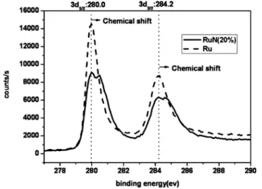
We also proved the existence of the RuN phases according to the result of XPS. Figure2shows that the binding energy of Ru peaks 共3d3/2: 284.2 eV, 3d5/2: 280.0 eV兲 was split and a part of them
shifted slightly to a higher value. This phenomenon was due to the fact that the Ru atoms were in different valence states, inducing the chemical shift. The stoichiometric composition of the RuN films was also measured by XPS, as shown in TableI. It is obvious that
the N content of the RuN films increased with the rise in the N2flow
ratio. The microstructures of the RuN films were examined by SEM. Figure3areveals that pure Ru has a column structure that has the paths for Cu diffusion during the annealing process. When the ni-trogen mixes in, the column size decreases and the phase transforms into RuN, as shown in Fig.3b. In addition, the grain size of Ru and RuN could be determined by Scherrer’s formula. Applying the XRD result of Fig.1binto the formula, we derived that the grain sizes of the Ru and RuN共20%兲 films were 12.73 and 5.85nm, respectively. Even though there are more grain boundaries in the RuN films than the Ru film, the grain boundaries in the RuN films do not extend from top to bottom, which could not provide direct diffusion paths for Cu. In contrast, the grain boundaries in the Ru films could pro-vide direct diffusion paths for Cu. As mentioned earlier, we consider that the RuN film with proper N content had a better antidiffuse ability than the pure Ru film.
Figure4shows that the resistivity of all RuN samples decreased after annealing. The resistivity of the high N-content samples共43, 50, and 56%兲 decreased rapidly when the annealing temperature was above 100°C. On the other hand, the resistivity of the low N-content samples共20 and 33%兲 decreased when the temperature was above 200°C. The N effusion rate was higher in the high N-content Figure 1.共a兲 Resistivity and deposition rate of the as-deposited RuN films.
共b兲 XRD spectra of the as-deposited RuN/Si substrates with different N2
flow ratios.
Figure 2. XPS spectra of the as-deposited pure Ru and RuN films.
Table I. Atomic ratio of Ru and RuN films.
Sputtering nitrogen ratio 共N2/N2+ Ar兲
共%兲 Ru atomic ratio共%兲 N atomic ratio共%兲
0 99.6 0.4 20 93.3 6.7 33 91.0 9.0 43 86.5 13.5 50 77.6 22.4 56 70.0 30.0
Figure 3. Microstructures of the as-deposited RuN/Si substrates with
differ-ent N2flow ratios:共a兲 0 and 共b兲 20%.
Figure 4. Resistivity of the RuN samples after annealing from 100 to 800°C.
samples because more nitrogen atoms did not bond with Ru atoms in the high N-content samples, whereas the nitrogen atoms in the low N-content samples almost bonded with Ru atoms.
Annealing also provides sufficient energy to decompose the un-stable Ru-N bonding and to transform the RuN film into the hex-agonal crystals. The XRD results of Fig.5show that the lower one
was the as-deposited RuN共56%兲 sample and the upper one was the sample annealed at 300°C. Ihara et al.11reported that there were a large amount of nitrogen vacancies in the RuN films after annealing. Not only hexagonal structures but also fcc ones were formed in the RuN films, meaning that there were fewer paths for Cu diffusion,
Figure 6. SEM images and AFM micrographs of共a兲 Ru/Si; 共b兲 RuN 共20%兲/
Si; and共c兲 RuN 共56%兲/Si after annealing at 300°C for 5 min.
Figure 7. SEM images and AFM micrographs of共a兲 Ru/Si; 共b兲 RuN 共20%兲/
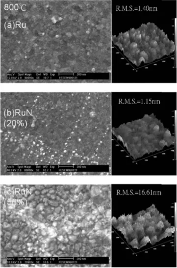
Si; and共c兲 RuN 共56%兲/Si after annealing at 800°C for 5 min.
Figure 8. Resistivity vs annealing temperature 共from 100 to 800°C兲 of
Cu/RuN/Si structures.
Figure 5. XRD results of the as-deposited RuN 共56%兲 sample and the
and this is why the RuN barrier had a better antidiffusion property even when the phase was changed after annealing. Furthermore, N atoms effused from the RuN films after annealing, and this may induce some unfavorable phenomenon on the surface of the RuN films. We can see from the SEM images shown in Figs.6and7that pure Ru and the low N-content 共20%兲 RuN films had smoother surfaces whereas the high N-content 共56%兲 RuN films became rougher after 300 or 800°C annealing. There were many bulges on the surface when the annealing temperature was set at 300°C. It was suspected that the worse thermal stability of the high N-content RuN films was due to a large amount of nitrogen vacancies after nitrogen effusion. As mentioned above, annealing provides sufficient energy
to transform the RuN films into hexagonal crystals, and defects were formed by nitrogen effusion at the same time. The effused N content could make some vacancies in the film, resulting in a rough surface after annealing. The AFM micrographs of Figs.6and7could sup-port the model.
Cu/RuN/Si structure.— We deposited a 50-nm thick Cu layer
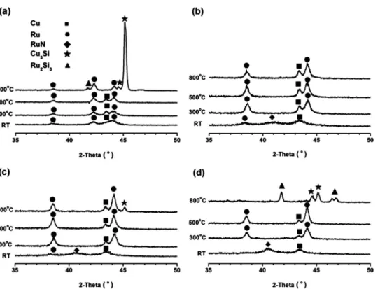
onto the RuN films to check their barrier properties for Cu diffusion. Figure8shows that the resistivity of the high N-content共43, 50, and 56%兲 RuN films rose steeply when the annealing temperature was above 700°C. In contrast, the resistivity increased slightly in the pure Ru and low N-content RuN films. It was suggested that the increase in the film resistivity was due to the formation of Cu sili-cide. In particular, the resistivity of the RuN共20%兲 sample only rose slightly even when the annealing temperature was higher than 800°C. In this case, we want to clarify the relationships between the crystalline structure and the diffusion behavior. Figure9shows the XRD results of the RuN films with different conditions after the annealing process. For the Cu/Ru/Si sample, both the Ru2Si3peak and the striking Cu3Si peak formed, and none of the Cu phase re-mained when the annealing temperature rose to 800°C. The pres-ence of Cu3Si demonstrated that Cu diffused into Si through the barrier layer.5,7,12-15A similar case is that there were both Ru2Si3 and Cu3Si peaks in the Cu/RuN 共56%兲/Si sample. Overall, the RuN
共20%兲 film had the best barrier property among the samples. There was no Cu silicide or Ru silicide remaining in the Cu/RuN 共20%兲/Si sample even after 800°C annealing. When the N2 flow ratio in-creased to 33%, the Cu3Si phase appeared, and there were still some
Ru and Cu phases remaining after annealing. Ru2Si3is currently an
imperfect product in the metallization process, which can adversely affect device quality. However, this study found that the optimiza-tion of nitrogen content in the RuN films reduced not only Cu dif-fusion but also the formation of Ru2Si3.
Electrodeposition of Cu on RuN.— Figure 10 shows the SEM top-view images of the nucleation behavior of Cu electroplating on different RuN substrates and plating times. It was found that small Cu clusters were reduced on the substrate at first and then gradually became larger with the plating time from 2 to 10 s. The Cu nucle-ation rate decreased with the rise of the N content; however, larger Figure 9. XRD textures of different RuN
films after annealing from 300 to 800°C for 1 h:共a兲 Cu/Ru/Si; 共b兲 Cu/RuN 共20%兲/ Si;共c兲 Cu/RuN 共33%兲/Si; and 共d兲 Cu/RuN 共56%兲/Si.
Figure 10. SEM images of electroplated Cu clusters on different RuN
Cu clusters were formed on the N-rich RuN substrates at the plating time of 10 s. In this study, both the Ru and RuN films were demon-strated to be a plateable layer for Cu electroplating. As the minimum feature size of microelectronic devices shrinks, the overall barrier and seed thickness were critical for the gap-filling process window of subsequent Cu electroplating process. The plateable RuN film could act as both a barrier and seed layers to reduce overall thick-ness as compared with the current Ta/TaN barrier and Cu seed layers. After Cu electroplating, we then used 3M Scotch packing tape to test the adhesion between the Cu and Ru/RuN substrates, and all of the samples remained intact after the test.
Conclusion
The RuN films deposited in the N2 and Ar atmospheres were
assessed as a good diffusion barrier for Cu. The resistivity of the RuN films decreased with increasing annealing temperature. How-ever, the RuN films with a too high N content had a rougher surface and more vacancies after annealing due to more nitrogen effusion. The diffusion of Cu through the RuN film was slower as compared with the Ru film because the RuN films had a less direct diffusion path for Cu as compared with the Ru film. However, when the N content was too high, too many vacancies may be formed after annealing due to nitrogen effusion, resulting in a poor barrier prop-erty for Cu diffusion. In this study, the 20% N2flow ratio was the
best condition for the RuN barrier properties. We also demonstrated that the Cu film could be directly electroplated on the RuN films with adequate adhesion.
Acknowledgments
The authors thank National Cheng Kung University, Tainan, Tai-wan, for its technical support.
References
1. M. Damayanti, T. Sritharan, Z. H. Gan, S. G. Mhaisalkar, N. Jiang, and L. Chanb,
J. Electrochem. Soc., 153, J41共2006兲.
2. T. P. Moffat, M. Walker, P. J. Chen, J. E. Bonevich, W. F. Egelhoff, L. Richter, C. Witt, T. Aaltonen, M. Ritala, M. Leskelä, et al., J. Electrochem. Soc., 153, C37 共2006兲.
3. O. Chyan, T. N. Arunagiri, and T. Ponnuswamy, J. Electrochem. Soc., 150, C347 共2003兲.
4. R. Chan, T. N. Arunagiri, Y. Zhang, O. Chyan, R. M. Wallace, M. J. Kim, and T. Q. Hurdc, Electrochem. Solid-State Lett., 7, G154共2004兲.
5. J. P. Chu, C. H. Lin, and V. S. John, Appl. Phys. Lett., 91, 132109共2007兲. 6. M. Damayanti, T. Sritharan, S. G. Mhaisalkar, H. J. Engelmann, E. Zschech, A. V.
Vairagar, and L. Chana, Electrochem. Solid-State Lett., 10, P15共2007兲. 7. C. W. Chen, J. S. Chen, and J. S. Jeng, J. Electrochem. Soc., 155, H438共2008兲. 8. M. Kawamura, K. Yagi, Y. Abe, and K. Sasaki, Thin Solid Films, 494, 240共2006兲. 9. M. Damayantia, T. Sritharan, S. G. Mhaisalkar, and Z. H. Gan, Appl. Phys. Lett.,
88, 044101共2006兲.
10. S. Ogawa, N. Tarumi, M. Abe, M. Shiohara, H. Imamura, and S. Kondo, in
Inter-connect Technology Conference, IITC 2008. International, p. 102共2008兲.
11. H. Ihara, N. Terada, K. Senzaki, M. Hirabayashi, Y. Kimura, R. Uzuka, F. Ka-washima, and M. Akimoto, IEEE Trans. Magn., 23, 1011共1987兲.
12. J. J. Tan, X. P. Qu, Q. Xie, Y. Zhou, and G. P. Ru, Thin Solid Films, 504, 231 共2006兲.
13. D. C. Perng, J. B. Yeh, and K. C. Hsu, Appl. Surf. Sci., 254, 6059共2008兲. 14. H. Kim, T. Koseki, T. Ohba, T. Ohta, Y. Kojima, H. Sato, and Y. Shimogakia, J.
Electrochem. Soc., 152, G594共2005兲.
15. S. H. Kwon, O. K. Kwon, J. S. Min, and S. W. Kang, J. Electrochem. Soc., 153, G578共2006兲.
16. M. Stavrev, D. Fischer, and F. Praessler, J. Vac. Sci. Technol. A, 17, 993共1999兲. 17. C. Ryu, A. L. S. Loke, T. Nogami, and S. S. Wong, IEEE Int. Reliab. Phys. Symp.