Improving the Performance of Transparent PLEDs
with LiF/Ag/ITO Cathode
Kou-Chen Liu,a,zChao-Wen Teng,a Yen-Hsun Lu,aJiun-Haw Lee,band
Lai-Cheng Chenc
a
Graduate Institute of Electro-optical Engineering, University of Chang Gung, Kwei-Shan Tao-Yuan 333, Taiwan
b
Graduate Institute of Electro-optical Engineering and Department of Electrical Engineering, Taiwan University, Taipei, Taiwan
c
Delta Optoelectronics, Incorporated, Hsinchu 30076, Taiwan
This work demonstrates the favorable performance of a transparent polymeric light-emitting diode 共PLED兲 using an effective LiF/Ag/indium tin oxide共ITO兲 cathode. An Ag layer can prevent the underlying emitting layer from damage by bombardment during ITO sputtering. Devices that have an Ag layer have a lower driving voltage and lower leakage current than those without. X-ray photoelectron spectroscopy data show that Ag increases the concentration of Li in the polymer, enhancing its electron injection and transport capacities. The lower leakage current results from the fact that the work function of Ag is lower than that of ITO. The insertion of the Ag layer also enhances the optical characteristics by improving carrier balance and reducing sputtering damage.
© 2007 The Electrochemical Society. 关DOI: 10.1149/1.2757116兴 All rights reserved.
Manuscript submitted May 3, 2007; revised manuscript received June 1, 2007. Available electronically July 19, 2007.
Organic light-emitting diodes共OLEDs兲 have attracted substantial attention because of their superior potential for use in flat-panel displays.1The next generation of flat-panel displays must be able to reproduce high-quality moving images, be lightweight, and consume little power. Furthermore, transparent OLEDs are expected to be useful in high-resolution full-color displays, as well as in helmet-mounted, windshield-mounted, or other “head-up” display applications.2The double-transparent electrode, such as indium tin oxide共ITO兲, is applied to achieve this objective. Although various methods are available for depositing ITO films,3-5sputtering depo-sition provides the benefits of high depodepo-sition rate and operating stability.6Furthermore, some investigations have demonstrated that using the sputtering process to deposit a contact electrode offers better adhesion than conventional thermal evaporation, facilitating a decline in the operating voltage, especially when an effective cath-ode such as Mg/Ag7is adopted. However, at high operating voltages the fact that the resistivity of ITO is higher than that of metal is a critical issue as it may be detrimental in microdisplay applications. Inserting a thin metal, such as Mg/Ag, Ca, or Li between ITO and the emitting layer has been considered to reduce the resistivity of ITO.8,9The purpose of this metal is to reduce not only the resistivity but also the height of the electron injection barrier and usually a metal with a low work function is used. However, such metals are not well-suited in the operating environment, because they are highly chemically reactive and therefore oxidize during sputtering of the ITO cathode.10Therefore, a new metal is sought to replace these low-work-function metals. Although the use of a noble metal may prevent oxidation, the fact that the high work function of the noble metal is likely to be associated with a large injection barrier should also be considered. Many efforts have been made to use widely adopted alkaline fluorides such as LiF, NaF, and CsF,11,12and espe-cially LiF to reduce the electron injection barrier height. Other re-searchers have also presented the benefits of using alkaline flourides such as chemical interaction, tunneling, and the interface dipole effect.13,14Additionally, the insertion of the metal buffer layer is also expected to improve the light output. Ag metal exhibits relatively low optical absorption and has the highest conductivity of almost all metals.15Smith et al.16also noted that inserting an Ag buffer layer can efficiently guide the light output while providing protection for the underlying emitting layer during the ITO cathode deposition. During sputtering, the bombardment of the energetic particles gen-erally induces the formation of defects and local trap sites, resulting
in the structural and electrical deterioration of organic films. There-fore, the thickness of the inserted metal is important and the metal must be able to prevent sputtering damage. According to Parthasar-athy et al.,17the thickness of the insertion metal governs both the transparency and the damage due to bombardment. In this work, Ag insertion metal is employed for its superior stability, conductivity, and optical characteristics; the cathode configuration LiF/Ag/ITO is used to fabricate transparent PLEDs with low operating voltage, high electroluminescence共EL兲 performance, and favorable protec-tion against sputtering damage.
The configuration of transparent PLED is ITO glass/poly 共3,4-ethylene dioxythiophene共PEDOT兲:poly共4-styrene sulfonate兲 共PSS兲/ polyfluorene共PFO兲/LiF/Ag/ITO. Because both electrodes are trans-parent, the light is emitted from the cathode and the anode. The ITO-glass substrates are cleaned by a treatment with O2plasma. The
polymer layers, PEDOT:PSS and PFO, are spin-coated and then baked in a nitrogen glove box containing less than 1 ppm oxygen and moisture. The sample is then transferred to the thermal evapo-ration chamber to deposit LiF and Ag, using an effusion cell and a heated resistor, respectively. The ITO cathode is deposited using a sputtering system. Finally, the devices are encapsulated in UV-curing epoxy resin. The transparency and resistivity of the LiF/Ag/ITO cathode are measured using a UV/visible/near-infrared 共NIR兲 spectrometer 共PerkinElmer Lamda 900兲 and a four-point probe共FPP 5000兲 to understand how the thickness of Ag influences these properties. The performance of the device is characterized us-ing Keithly-2430 and Keithly-6485 measurement systems in an at-mosphere of air at room temperature. The luminance is measured from both the anode and the cathode sides. X-ray photoelectron spectroscopy共XPS兲 measurements are made using a Perkin Elmer ESCA 5400 to elucidate the damage caused by bombardment during the sputtering of the ITO cathode.
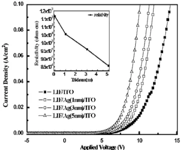
Figure 1 demonstrates that inserting an Ag layer improves the current density-voltage共J-V兲 characteristic. The turn-on voltage of the devices, defined as the bias at which the current density is 1 mA/cm2, is 5.8, 5.5, and 4.8 V for devices with Ag layers of 1, 3,
and 5 nm thickness; the corresponding voltage reduction percent-ages are 10, 15, and 26% from the voltage of the device with the LiF/ITO cathode. Such a voltage reduction is associated with 共i兲 lower resistance of the Ag/ITO electrode,共ii兲 better injection from the cathode to the PFO,共iii兲 better electron transport capability in the PFO emitting layer关electromodulation of luminescence 共EML兲兴, and共iv兲 lower ion bombardment. Because the conductivity of Ag is two orders of magnitude higher than that of ITO, the resistivity of the electrode is substantially reduced when a thin Ag layer is intro-duced into the ITO thin film.15The inset in Fig. 1 plots the
resistiv-z
E-mail: jacobliu@mail.cgu.edu.tw
Electrochemical and Solid-State Letters, 10共10兲 J120-J122 共2007兲
1099-0062/2007/10共10兲/J120/3/$20.00 © The Electrochemical Society
J120
ity of the LiF/Ag/ITO layer on the Si/SiO2wafer, which declines monotonically as the Ag thickness increases from 1–3 to 5 nm. Kido et al. reported that the incorporation of Li into the organic materials can significantly improve the injection barrier from the cathode to the electron transport layer 共ETL兲 and the electron transport characteristics.18Although the Li ion is believed to be released from the LiF layer, numerous works have reported that Ag does not react with LiF, because more heat is produced between LiF and Ag than by Al. However, the sputtering process of ITO deposition may pro-vide the energy to overcome the reaction enthalpy. The sputtering process transforms kinetic energy to heat, which can activate the LiF/Ag reaction. A thicker Ag layer provides more Ag to react with LiF, liberating more Li to dope the emitting layer, as verified by XPS data. This reaction is similar to the LiF/Al reaction which was presented in previous works.13,14Table I also shows that the concen-tration of Li in the EML increases with Ag thickness, providing direct evidence of the Li doping result. Additionally, inserting an Ag layer improves not only the electrical characteristics but also the optical properties, which are discussed later. The Ag layer is an effective buffer layer that prevents the formation of quench centers by sputtering damage and prevents exciton quenching. XPS mea-surements were made to characterize the phenomenon penetration into the emitting layer during sputtering ITO deposition. The com-positions of ITO which include indium共In兲, tin 共Sn兲, and oxygen 共O兲 decreased sharply when a 1 nm thick Ag layer was inserted and continued to fall as the thickness of Ag was increased, as presented in Table I. This result indicates that the Ag film sufficiently prevents the impingement by high-kinetic-energy particles of In, Sn, and O. It also demonstrates that even a 1 nm thick layer used as the buffer layer can sufficiently suppress the sputtering bombardment into the
emitting layer. For these two reasons, the devices with Ag layers have a higher current efficiency than those without. Figure 2 plots the leakage current density at −5 V for various Ag thicknesses. The insertion of an Ag layer with a thickness of 1 nm increases the leakage current to double that in the LiF/ITO case. The leakage current decreases rapidly as the Ag thickness increases. When the Ag thickness is 5 nm, the leakage current is even lower than the LiF/ITO case. This work proposes a possible mechanism of this behavior. When the Ag layer is thin, 1 or 3 nm, the ITO sputtering process oxidizes the Ag to form AgxO, which has a high work function.15 Under reverse bias, the holes can be injected through these AgxO sites into the PFO, explaining the first increase in the leakage current when a thin Ag layer of 1 or 3 nm is inserted be-tween the LiF and ITO. As the Ag thickness increases, the leakage current declines because the Ag/AgxO ratio increases. When the Ag film is 5 nm, the leakage current is even lower than that of ITO, because the lower work function of Ag is responsible for a higher barrier to the hole current under reverse bias, as presented in the inset in Fig. 2. Moreover, the presence of LiF also contributed to a high barrier to the hole current at reverse bias. According to our earlier investigation共not shown here兲, the device with an ITO cath-ode has a higher leakage current of 3.4⫻ 10−6A/cm2. Figure 3
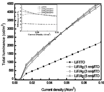
displays the total brightness, obtained by summing the top and bot-tom outputs of the transparent PLEDs. The brightness of devices with Ag buffer layers markedly exceeds that of those without. This result can be explained by the shift in the dipole recombination due to the lower resistivity of the cathode and the lower sputtering dam-age. The resistivity of the cathode is reduced when an Ag layer is inserted, strengthening the electrical field across PFO at a fixed volt-age. Hence, the dipole recombination deposition shifts toward the HTL/EML interface. The dipole recombination region shifts far from the cathode, preventing electrode quenching and Li-diffusion quenching, which have been discussed elsewhere.19Although de-vices with Ag layers all perform similarly and exhibit high lumi-nance, the top/bottom emitting luminance ratio varies significantly with the Ag thickness in the devices, as shown in Fig. 4. The top/ bottom ratio initially increases when an Ag layer is inserted and then declines as the Ag thickness increases. As stated above, the incor-poration of Ag shifts the recombination zone toward the HTL/EML interface and reduces the quenching effect at the cathode共top side兲. Therefore, the top emission from devices with Ag thickness of 1 nm exceeds that from LiF/ITO. The total emission of the OLED with Ag thickness of 1 nm is double that without Ag 共Fig. 3兲, but the top/bottom ratio is only 60% higher共Fig. 4兲, because the Ag film reflects some of the top-emitting photons and contributes to the bot-tom emission. According to Han et al.,20increasing the metal
thick-Figure 1. Current-voltage characteristic of transparent PLEDs with different
thicknesses of Ag. The insertion is the resistivity of samples structure of Si/SiO2/Ag/ITO.
Table I. The elements distribution of samples with different Ag thicknesses.
Sample structure The element in PFO
PFO/LiF/Ag/ITO In共%兲 Sn共%兲 O共%兲 Li共%兲 F共%兲
Ag共0 nm兲 14.27 1.01 3.6 3.59 8.77
Ag共1 nm兲 8.33 0.42 2.29 4.8 14.54
Ag共3 nm兲 4.17 0.27 2.1 5.6 12.24
Ag共5 nm兲 2.49 0.11 1.4 8.03 10.06
Figure 2. Leakage current variation with different Ag thicknesses.
J121 Electrochemical and Solid-State Letters, 10共10兲 J120-J122 共2007兲 J121
ness drastically reduces resistivity and optical transparency. Figure 4 also demonstrates that the transparency of the cathode decreases as the Ag thickness increases. This result is consistent with Han’s. Hence, the increase in reflectance associated with an increase in Ag thickness is conjectured to intensify the emission from the bottom side and the lower transparency is conjectured to reduce the light from the top side. Therefore, the emission ratio is reduced. However, further work is required to accurately detail the behavior of the internal waveguide.
This study demonstrates the favorable performance of transpar-ent PLEDs with a thin Ag buffer layer. The presence of an Ag layer tunes the work function of the interface of the cathode not only to facilitate electron injection but also to suppress the leakage current. Additionally, inserting an Ag layer shelters the organic emitting layer from damage due to sputtering bombardment during the depo-sition from the top cathode, even when the Ag layer is thin.
Acknowledgments
The authors thank Delta Optoelectronics, Incorporated of Hsin-chu, Taiwan, for supporting this research and Chung Shan Institute of Science and Technology共CSIST兲 for the facilitation of XPS mea-surements.
Chang Gung University assisted in meeting the publication costs of this article.
References
1. H. W. Choi, S. Y. Kim, K.-B. Kim, Y.-H. Tak, and J.-L. Lee, Appl. Phys. Lett., 86, 012104共2005兲.
2. M. Pfeiffer, S. R. Forrest, X. Zhou, and K. Leo, Org. Electron., 4, 21共2003兲. 3. H.-K.Kim, K.-S. Lee, M.-J. Geum, and K.-H. Kim, Electrochem. Solid-State Lett.,
8, H103共2005兲.
4. C. H. Chung, Y. W. Ko, Y. H. Kim, C. Y. Sohn, H. Y. Chu, and J. H. Lee, Appl. Phys. Lett., 86, 093504共2005兲.
5. T. C. Gorjanc, D. Leong, C. Py, and D. Roth, Thin Solid Films, 413, 181共2002兲. 6. T. Minami, H. Sonohara, T. Kakumu, and S. Takata, Thin Solid Films, 270, 37
共1995兲.
7. H. Suzuki and M. Hikita, Appl. Phys. Lett., 68, 2276共1996兲.
8. G. Gu, V. Bulovi, P. E. Burrows, S. R. Forrest, and M. E. Thompson, Appl. Phys. Lett., 68, 2606共1996兲.
9. L. S. Hung and J. Madathil, Thin Solid Films, 410, 101共2002兲.
10. K. Tominaga, M. Chong, and Y. Shintani, J. Vac. Sci. Technol. A, 12, 1435共1994兲. 11. J. Lee, Y. Park, D. Y. Kim, H. Y. Chu, H. Lee, and L. M. Do, Appl. Phys. Lett., 82,
173共2003兲.
12. S. L. Lai, M. Y. Chan, C. S. Lee, and S. T. Lee, J. Appl. Phys., 94, 7297共2003兲. 13. M. G. Mason, C. W. Tang, L.-S. Hung, P. Raychaudhuri, J. Madathil, D. J. Giesen,
L. Yan, Q. T. Le, Y. Gao, S.-T. Lee, et al., J. Appl. Phys., 89, 2756共2001兲. 14. L. S. Hung, C. W. Tang, and M. G. Mason, Appl. Phys. Lett., 70, 152共1997兲. 15. C. W. Chen, P. Y. Hsieh, H. H. Chiang, C. L. Lin, H. M. Wu, and C. C. Wu, Appl.
Phys. Lett., 83, 5127共2003兲.
16. L. H. Smith, J. A. E. Wasey, and W. L. Barnes, Appl. Phys. Lett., 84, 2986共2004兲. 17. G. Parthasarathy, C. Adachi, P. E. Burrows, and S. R. Forrest, Appl. Phys. Lett.,
76, 2128共2000兲.
18. J. Kido and T. Matsumoto, Appl. Phys. Lett., 73, 2866共1998兲.
19. L. S. Hung, L. S. Liao, C. S. Lee, and S. T. Lee, J. Appl. Phys., 86, 4607共1999兲. 20. S. Han, D. Grozea, C. Huang, and Z. H. Lu, J. Appl. Phys., 96, 709共2004兲. Figure 3. Total luminance共the sum of light from top and bottom兲 of devices
with different Ag thicknesses.共Inset兲 Current efficiency vs current density.
Figure 4. Transparency共at 540 nm兲 of cathode and emitting ratio of device
with different Ag thickness.
J122 Electrochemical and Solid-State Letters, 10共10兲 J120-J122 共2007兲 J122