行政院國家科學委員會專題研究計畫 成果報告
應用於多種無線通訊系統之寬頻天線陣列
研究成果報告(精簡版)
計 畫 類 別 : 個別型
計 畫 編 號 : NSC 95-2221-E-002-092-
執 行 期 間 : 95 年 08 月 01 日至 96 年 07 月 31 日
執 行 單 位 : 國立臺灣大學電信工程學研究所
計 畫 主 持 人 : 鄭士康
計畫參與人員: 博士班研究生-兼任助理:蔡志勇、周厚原、賴明佑
報 告 附 件 : 出席國際會議研究心得報告及發表論文
出席國際會議研究心得報告及發表論文
處 理 方 式 : 本計畫可公開查詢
中 華 民 國 96 年 08 月 23 日
應用於多種無線通訊系統之多頻段天線陣列
A multi-band antenna array for multiple wireless
communication systems
計畫編號
NSC95-2221-E-002-092
執行期限:95 年 8 月 1 日至 96 年 7 月 31 日
主持人:鄭士康 台大電信工程研究所
計畫參與人員:蔡志勇,周厚原,賴明佑
台大電信工程研究所
中文摘要 近年來無線通訊產品大量湧現在生活週 遭的每一個角落,慢慢地成為人們生活中不可 或缺的物品。為達到更優質的通訊,各式各樣 的基地台和橋接器的需求逐漸增加。如果每一 個通訊系統都使用各自的基地台或橋接點,週 遭環境中所需安裝的天線數目將大量增加,眾 多天線的架設亦有礙觀瞻。本研究計畫設計完 成一個適用於各種通訊系統、價廉、精巧的多 功能寬頻相位陣列天線系統。該架構由兩個四 天線元件的陣列所組成。鑒於大部分的無線通 訊使用的頻譜分布在 2.0GHz 到 6.0GHz 之 間,因此我們設計一個工作於此頻帶範圍之陣 列天線作為範例。量測結果顯示:除3GHz 以 下範圍,由於天線耦合較強,場型不如預期 外,其餘頻段測得結果均與設計相符。 關鍵字:陣列天線 AbstractIn this project a new wideband array antenna system for multiple wireless applications is developed. It is composed of two equispaced four-element arrays, phase shifters, diplexers, and power dividers. The two arrays are interleaved and connected to diplexers and power dividers. The proposed antenna system associated with feeding network and antenna elements can be integrated on a single substrate. Consequently, such a design is with low fabrication and assembly cost and compact size. A wideband antenna array with bandwidth from 2.0GHz to 6.0GHz and main beam pointing to 20 degrees is designed and measured as an example. The radiation patterns below 3.0GHz deforms drastically, suffering from mutual couplings between antenna elements. The performance for other frequencies seems to agree with our design.
Keywords: array antenna.
I. Introduction
Recently wireless communication products emerge in large number and gradually become living essentials. The demand of various base stations and access points for different communication standards increases in order to pursue better service quality. As the number of base stations and access points goes up, the number of antennas increases dramatically. Technically, it results in serious couplings between antennas of different communication systems and occupies a large space. For the public, it arouses concerns about their excessive electromagnetic radiation. Thus, a compact multifunctional array antenna to provide a wide variety of wireless services is highly desired.
Consider an equispaced array of 4 elements, a uniform progressive phase factor δ can be introduced to position the main beam to angles θ0 and π-θ0 [1]. If δ is a linear function of
frequency, the direction of main beam still points at θ0 and π-θ0, but the main beam deforms and
the level of side lobe degrades as frequency sweeps. The digital signal processing technique, digital beamforming, can provide a frequency-invariant beam pattern over an arbitrary bandwidth [2]. This approach is very powerful, but for an n-element array each antenna requires an RF transceiver and A/D converter, resulting in high fabrication cost. Consequently, designing an array with lower cost and beam pattern not sensitive to frequency sweeping is in great demand for future wireless applications.
Here we propose a new wideband array antenna system which is composed of two equispaced four-element arrays, phase shifters, diplexers and power dividers. The two arrays are interleaved and connected to diplexers and
power dividers. The proposed antenna system associated with feeding network and antenna elements can be integrated on a single substrate, offering lower fabrication and assembly cost and more compact size than the conventional solutions. A wideband antenna array with bandwidth from 2.0 GHz to 6.0 GHz and main beam pointing to 20 degrees is designed and measured as an example.
II. Design Concept
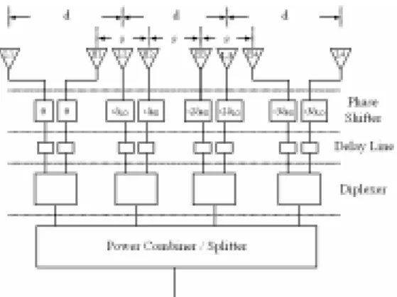
The structure of the proposed system is depicted in Fig. 1. The phase shifters are designed to position the main beam to a specific direction. The use of the diplexers is to switch the two arrays as frequency sweeps. Assume that
f1 and f2 are the lowest and the highest
frequencies of the desired band, choose
2 1f f fc= (1)
(
)
2 1 c LO f f f = + (2)(
)
2 2 c HI f f f = + (3)Such a choice makes the low- and high-bands of the diplexer have the same fractional bandwidth. The frequency response of the diplexer is plotted in Fig. 2. The delay lines in Fig.1 are designed so that the outputs of the
diplexer are with the same phase at fc. Finally,
the diplexers are fed using wideband power dividers.
The array factor of the proposed system can be expressed in the form
( ) ( )
∑
( ) ( )∑
( ) = − = − + ⋅ ⋅ = 4 1 sin 0 4 1 sin 0 , n HI s k jn HI n LO d k jn LO f e C f A e C f AF θ θδ θδ (4) HI LO HI LO f f , , δ δ = (5) ( )sinθ 0 2 3k ds j e A= − (6) wherek0 wave number in free space;
d and s half-wavelengths in free space at frequencies fLO and fHI, respectively; CLO and CHI frequency responses of the low-band
and the high-band of the diplexer, respectively;
δ system progressive phase factor, a constant;
δLO and δHI progressive phase factors of array
with spacing d and s, respectively.
CLO and CHI are similar to the responses of
bandpass filters with center frequencies at fLO
and fHI, respectively. The array with spacing d
works as frequency being around fLO , and the
array with spacing s works as frequency being around fHI . By introducing the diplexers, the
deformation of the main beam due to frequency sweep can be relieved.
III. Simulation and Measurement Results
A. Simulation Results
A 2.0 GHz to 6.0 GHz wideband antenna array with mainbeam pointing to 20 degrees is designed to validate the proposed concept. According to the equations in Section II, δ=61 degrees, fc=3.46 GHz, fLO=2.73 GHz and fHI=4.73 GHz. The spacings d and s are 54.9 mm
and 31.7 mm, respectively. The minimal spacing between two antenna elements is 11.6 mm, corresponding to 0.13λ0 at fc. Assume that the
mutual couplings between antenna elements can be neglected, the simulated array factors are plotted in Fig. 3, and the side lobe level against frequency and the 3dB beamwidth against frequency are shown in Fig. 4. It is seen that the main beam points to 20 degrees over 2.0 GHz to 6.0 GHz, the 3dB beamwidth is between 22o and
38o, and the side lobe level is larger than 10 dB
from 2.0 GHz to 5.7 GHz.
B. Components Design
The substrate used is an RO4003 with
Fig.1. Proposed System Architecture.
thickness 0.508 mm and relative dielectric constant 3.38. As discussed previously, the minimal spacing between two antennas is 11.6 mm. As a result, an antenna element with a width smaller than 11.6 mm is needed. However, the design of such a planar antenna with a bandwidth from 2.0 GHz to 6.0 GHz presents many difficulties. One of possible solutions is a loaded monopole antenna, offering a compact size and excellent pattern characteristics over a wide bandwidth. The resultant antenna element is shown in Fig. 5. The antenna gain between 2.0GHz to 6.0 GHz is 1.0dBi in average. Figure 6 presents the couplings between antenna elements, showing that the maximum coupling is -6 dB.
For the diplexer, we connect two broadband bandpass filters based on stub-line filters [3]-[7] together to form the desired diplexer; nevertheless, some unwanted interactions between the filters cause serious performance degradation. As a result, we develop a Matlab program based on fmins subroutine to optimize the designed parameters to meet the desired specifications. Figure 7 presents the layout and
scattering parameters of the designed diplexer. The losses at 2.0 GHz and 6.0 GHz are 0.3 dB and 0.8 dB, respectively. The measured cutoff frequency is at 3.45 GHz, which is almost identical to the simulated one. The measured and simulated phase differences at 3.45 GHz is 32 and 20.7 degrees, respectively. The discrepancy is contributed by the imperfection of the manually soldered SMA connectors at the output ports.
C. Feeding Network
The layout of the feeding network is shown in Fig. 8. Its size is 200 mm by 90mm. The 4-way power divider [8] and the four diplexers are connected together. The delay lines are used to make the outputs of the diplexers have the same phase at the cutoff frequency. The serpentine lines are designed to implement the phase shifters, making the differences between Ports Li and Li+1 at 2.73 GHz and between Ports Hi and Hi+1 at 4.73 GHz be 61 degrees,
respectively. Figure 9 presents the measured reflection coefficients and the insertion losses at output ports of the feed network. Ideally, the
Fig.5. Antenna element. (a) Geometry. (b) Amplitude of
S11..
Fig.6. Couplings between antenna elements.
Fig.7. Frequency responses of the diplexer used in the array system.
Fig.3. Simulated array factors of the proposed array system.
Fig.4. Side lobe level and 3dB beamwidth against frequency.
insertion losses at the output ports are -6dB. The additional losses at 2.0 GHz and 6.0GHz are 0.5 dB and 1.5dB, respectively, which are contributed by the 4-Way power divider and diplexers.
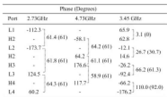
Table I summaries the measured phases at the output ports and phase differences between output ports at frequencies 2.73 GHz, 3.45 GHz, and 4.73 GHz. The numbers in brackets represent the ideal value. At the column of 3.45 GHz, the ideal phase shift between Ports Li and Hi can be determined by Eq. (7). It can be seen
that the measured phase shifts agree well with the designed ones.
− ⋅ ⋅ = ∆ HI LO i H i L f f i 1 1 , δ (7) D. Antenna Array
Figure 10 shows the radiation patterns in the
xy-plane at different frequencies. The radiation
patterns below 3.0 GHz deform dramatically,
suffering from mutual couplings between antenna elements.
V. Conclusions
A new wideband planar antenna array has been proposed in this paper. This antenna system associated with feeding network and antenna elements can be integrated in a single substrate. Consequently, such a design is with low fabrication and assembly cost and compact size. So far, the prototype of the array antenna has been completed. Suffering from the strong mutual coupling between antenna elements, the radiation patterns below 3 GHz deform dramatically. The overall system will be improved in the future.
References
[1] R. S. Elliott, Antenna Theory and Design Revised
Edition, Wiley-Interscience, 2003, Ch 4.
[2] D. H. Tuan and Peter Russer, “Signal Processing for Wideband Smart Antenna Array and Applications,”
IEEE Microwave Magazine, pp. 57-67, Mar. 2004.
[3] G. L. Matthaei, L. Young, and E. M. T. Jones,
Microwave Filters, Impedance-Matching Networks, and Coupling Structures, McGraw-Hill, 1964, Chapter
16.
[4] S. Srisathit, S. Patisang, R. Phromoloungsri, S. Bunnjaweht, S. Kosulvit, and M. Chongcheawchamnan, “High isolation and compact size microstrip hairpin diplexer,” IEEE Microwave and Wireless Comp. Lett., vol. 15, pp. 101-103, Feb. 2005.
[5] B. Strassner and K. Chang, “Wide-Band Low-Loss High-Isolation Microstrip Periodic-Stub Diplexer for Multiple-Frequency Applications,” IEEE Trans.
Microwave Theory Tech., vol. 49, pp. 1818-1820, Mar.
2001.
[6] D. M. Pozar, Microwave Engineering, John Wiley & Sons, 1998, Chap. 8.
[7] J. S. Hong and M. J. Lancaster, Microstrip Filters for
RF/Microwave Applications, John Wiley & Sons, 2001.
[8] S. B. Cohn, “A Class of Broadband Three-Port TEM-Mode Hybrids,” IEEE Trans. Microwave and
Tech., vol. 16, pp. 110-116, Feb. 1968.
Fig.8. Layout of the feeding network.
Fig.9. Measured reflection coefficient and the insertion losses at the output ports of the feeding network.
Fig.10. Measured radiation patterns of the designed antenna array.