國 立 交 通 大 學
光 電 工 程 研 究 所
博 士 論 文
高效率近紫外光發光二極體元件製作
Fabrication of High Efficiency Near-Ultraviolet
Light Emitting Devices
研 究 生:凃博閔 Student:Po-Min Tu
指導教授:張俊彥 教授 Advisor:Prof. Chun-Yen Chang
冉曉雯 教授 Prof. Hsiao-Wen Zan
高效率近紫外光發光二極體元件製作
Fabrication of High Efficiency Near-Ultraviolet
Light Emitting Devices
研 究 生:凃博閔 Student:Po-Min Tu
指導教授:張俊彥 教授 Advisor:Prof. Chun-Yen Chang
冉曉雯 教授 Prof. Hsiao-Wen Zan
國 立 交 通 大 學
光 電 工 程 研 究 所
博 士 論 文
A dissertation
Submitted to Institute of Electro-Optical Engineering College of Electrical Engineering and Computer Science
National Chiao-Tung University in Partial Fulfillment of the Requirements
for the Degree of Doctor of Philosophy
in
Electro-Optical Engineering June 2012
Hsinchu, Taiwan, Republic of China
中華民國一百零一年六月
高效率近紫外光發光二極體元件製作
研究生:凃博閔 指導教授: 張俊彥 教授
冉曉雯 教授
國立交通大學光電工程研究所
摘要
近年來,由於氮化鎵近紫外光發光二極體(near-UV LED)具有非常大的發展潛力及 廣泛應用,如驗鈔、光觸媒除臭、空氣淨化器等紫外光光源的使用,因此越來越多的團 隊開始研究高效率元件的製作及使用近紫外光於固態照明與螢光粉轉換光源之應用。 然而,低銦含量下的發光二極體其內部量子效率(IQE)驟降迅速,晶格品質與氮化 鎵自我吸收的問題更導致製作高效率近紫外光發光二極體是相當困難的。文獻指出低銦 含量氮化銦鎵(InGaN)量子井設計中,使用氮化鋁鎵(AlGaN)的位障來提高載子局限能力 是必須的;但由於此兩材料氮化銦鎵(InGaN)及氮化鋁鎵(AlGaN)最佳化的成長溫度大不 相同,因此深深的影響了兩者的晶格品質及其元件效率的表現。 此外,由於相對低價格及高品質的優點,藍寶石(Sapphire)是目前最廣泛使用於氮化 鎵材料的磊晶基板,但由於其導電性及導熱性差的特性致使元件的表現及設計處處受限。 近年來,許多研究團隊致力於發展雷射剝離 laser lift-off (LLO)技術,及使用氮化鉻(CrN)、 氧化鋅(ZnO)及矽摻雜氮化鎵(Si:GaN)等犧牲層來實現化學剝離 chemical lift-off (CLO)技 術,來實現獨立的氮化鎵薄膜及垂直式發光二極體元件製作,以提升更高的光電元件品 質與效率。然而,高溫的雷射剝離製程將導致氮化鎵/藍寶石(GaN/sapphire)界面及保護 層因熱衝擊而受損,進而造成元件漏電及低良率等問題;化學剝離製程雖然能避免雷射瞬間高溫加熱元件造成傷害,卻也造成後續蝕刻傷害及使用犧牲層造成晶格品質的問 題。
本論文中,我們利用氮化鋁鎵銦(InAlGaN)來取代原本的氮化鋁鎵(AlGaN)的位障以 實現高效率的近紫外光發光二極體,並開發一種使用倒六角錐結構 Hexagonal Inversed Pyramid (HIP)來實現機械式剝離 mechanical lift-off (MLO)製程以製作高品質氮化鎵垂直 式發光二極體(Vertical-LED),此外效率驟降的物理意義、剝離的機制及其光電特性分析 也將與本論文中有詳細的量測及調查。 首先,我們調查量子井中以氮化鋁鎵(AlGaN)及氮化鋁鎵銦(InAlGaN)為位障之氮化 銦鎵(InGaN)近紫外光發光二極體效率驟降的表現,電致發光(Electroluminescence)結果 顯示使用四元化合物材料(quaternary)的 LED 發光強度於 350 mA 及 1000 mA 電流操作 下分別提升了 25 %及 55 %,更進一步的物理模擬顯示使用四元化合物材料的 LED 於高 電流注入下提升了 62 %的輻射再結合率及 13 %較少的效率驟降,推測這些改善來自於 載仔濃度的提升及載仔更均勻的重新分佈。 再者,我們使用倒六角錐結構來實現機械式剝離製程以製作高品質氮化鎵垂直式發 光二極體,倒六角錐結構的製作採用高溫氫氧化鉀(KOH)濕蝕刻其氮化鎵/藍寶石基板的 界面來完成,TEM 分析結果顯示平均的線缺陷密度估計從 2×10⁹ 降低至 1×108 cm−2, 拉曼(Raman)光譜也揭露出使用倒六角錐結構的氮化鎵磊晶層之壓應力能有效的被釋放, 最後我們成功的使用倒六角錐結構為犧牲層並於晶片鍵合降溫過程中實現了機械式剝 離製程,其中剝離的物理機制、材料及元件的光電特性也將於本論文中詳細探討。
Fabrication of High Efficiency Near-Ultraviolet Light Emitting Devices
Student : Po-Min Tu Advisor : Prof. Chun-Yen Chang
Prof. Hsiao-Wen Zan
Department of photonics & Institute of Electro-Optical Engineering
National Chiao-Tung University
Abstract
GaN-based near-ultraviolet light emitting devices (LEDs) have attracted great attention in last few years due to its potential applications in photo-catalytic deodorizing such as air conditioner, and there have been interests in solid-state lighting by using near-UV LEDs light for the phosphor-converting source. However, it is difficult to fabricate near-UV LEDs with high efficiency, because the internal quantum efficiency (IQE) decreases drastically under the low indium composition.
Moreover, crystalline quality and light absorption of GaN are significant for short wavelength near-UV LEDs. It’s well known that in low indium content InGaN QWs, AlGaN barrier is necessary for carrier confinement. But the two materials of AlGaN and InGaN are very different in growth temperature which affects strongly on the quality of material and device performances.
In addition, the sapphire is the most commonly used substrate because of its relative low cost, but it also limits the devices performance due to its poor electrical and thermal conductivity. During the last decade of years, the techniques of laser lift-off (LLO) and chemical lift-off (CLO) which use CrN layer, ZnO layer, and Si-doped n-GaN layer as the sacrificial layer have been adopted to fabricate the freestanding GaN membrane and the vertical LEDs (V-LEDs) for the purpose of high performance optoelectronic devices.
However, the LLO process may induce some possible damages under high temperature in the GaN/sapphire interface. And even though the CLO can prevent the GaN layer from the laser damage during the laser lift-off process, but it also makes another chemical etching damages and reduce the crystal quality. Hence, we study the fabrication of mechanical lift-off (MLO) for high quality GaN-based V-LEDs with Hexagonal Inversed Pyramid (HIP) structures.
In this study, we demonstrate high efficient near-UV LEDs by replacing AlGaN by InAlGaN barrier in active region and mechanical lift-off technology. Furthermore, the efficiency droop characteristics, theoretical analysis of lift-off process, and optoelectronic properties of high efficient near-UV LEDs have been measured and investigated.
First, the efficiency droop in InGaN-based near-UV LED with AlGaN and InAlGaN barrier is investigated. Electroluminescence results indicate that the light performance of quaternary LEDs can be enhanced by 25 % and 55 % at 350 mA and 1000mA, respectively. Furthermore, simulations show that quaternary LEDs exhibit 62 % higher radiative recombination rate and low efficiency degradation of 13 % at a high injection current. We attribute this improvement to increasing of carrier concentration and more uniform redistribution of carriers.
Second, we report the fabrication of mechanical lift-off high quality GaN-based V-LED with HIP structures. The HIP GaN/air/Sapphire structures were formed at the GaN/sapphire substrate interface under high temperature during KOH wet etching process. The average threading dislocation density (TDD) was estimated by transmission electron microscopy (TEM) and found the reduction about one order. Raman spectroscopy revealed that the compressive stress of GaN epilayer was effectively relieved in the GaN-based LED with HIP structures. Finally, the mechanical lift-off process is claimed to be successful by using the HIP structures as a sacrificial layer during wafer bonding process. Furthermore, theoretical analysis of lift-off process, and optoelectronic properties of devices have been investigated.
誌謝
時光荏苒,一轉眼我在交大已經過了四年多的研究生活,終於畢業這一刻即將來臨, 穿上博士畢業服那一刻,心情頓時百感交集。 首先,我要感謝張俊彥校長和冉曉雯教授的細心指導,謝謝老師提供了很好的研究 環境與機會,總是在我最無助的時候給了我一股正向的力量,讓我勇敢往前進,持續做 對的事情。謝謝冉老師給予我研究上最大的空間與自由度,並感謝張校長帶著我走過人 生中最精彩的每一刻,重新賦予我生命的彩度。 研究生涯中,我遇到了許多的貴人:感謝楊宗熺博士的鼓勵與支持,讓我有機會完 成博士學位;感謝郭浩中老師無私奉獻所學及研究資源全力相挺,讓我的研究非常順利, 這一切我會銘記在心;感謝程育人老師教導我嚴謹的研究態度,還有善解人意與追根究 柢的精神讓人深感佩服;感謝林建中老師細心指導,並且不厭其煩的修改論文與研究方 向;感謝盧廷昌老師在研究中給予正確的研究方向與實驗靈感。 更要謝謝實驗室曾經幫助我的同學及學弟妹:感謝張哲榮同學從資格考開始一路陪 著我成長、漫漫長夜的討論與促膝長談至今仍然懷念,你對實驗室的付出與關懷,讓我 代表全實驗室說聲“謝謝”;感謝張世邦同學一句話情義相挺至今,犧牲奉獻陪著大家 一起努力做好研究;感謝凱麟、祐誠、昀瑾、婉儀、祥修、國斌、盈臻、小杜、芝羽、 柏君、江耀、博文,我的博士研究生涯因為有你們而變得豐富寬廣。還要感謝邱鏡學同 學,總是陪我一起熬夜考試、趕做報告、研究討論,幫我扛了很多繁雜的工作…這個博 士學位應當分你一半;還有李鎮宇博士、羅明華博士、陳士偉博士、李金釵博士、邱清 華博士、陳振昌博士、黃延儀博士、許世杰博士、江松柏、宋兆峯、洪誌彰、黃彥棠, 與你們一起研究的生活真的很精彩。後顧之憂能全心投入做研究;感謝黃世晟處長嚴謹與細心的教導,並將畢生磊晶的功力 傳授給我,在此說聲“謝謝師父”;感謝每一位同事及同學在我攻讀博士期間能體諒與 支持,謝謝順貴、梓健、佳輝、雅雯、鈺如、嘉宏、雅文、宜庭、美玲、亞琦、振安、 凌帆、穎超、芃逸、文禹、馬哥、宗民、慶昌、范文郎博士、范文忠博士、陳永翔博士; 還要感謝前輩照顧:詹世雄博士、曾堅信博士、張忠民博士、孫健仁博士、謝于誠副總。 另外,也感謝口試期間給予細心指導的蘇炎坤校長、張翼教授、張守進教授、黃建 璋教授,這些寶貴的建議將使本論文更加完整。 最後,感謝我的家人:阿嬤、父母、姐姐、姑姑,因為有你們精神上的支持,讓我 能全心全力的完成博士學位,真的很感謝你們。另外,這本書也獻給默默陪伴著我最愛 的怡汶及關心我支持我的每一個人,沒有你們,我是無法獨自完成這本論文,衷心的謝 謝你們。 凃博閔 于 101 年 6 月 28 日 交通大學光電工程研究所
Contents
Abstract (in Chinese) i
Abstract (in English) iii
Acknowledgement (in Chinese) v
Contents vii
List of Figures x
List of Tables xv
Chapter 1 Introduction ... 1
1.1 Wide Bandgap Ⅲ-Nitride Materials ... 1
1.2 GaN-based Near-Ultraviolet Light-Emitting Diodes (Near-UV LEDs) ... 2
1.3 Content of Dissertation ... 9
Chapter 2 Properties of InGaN-based Near-UV LEDs... 11
2.1 Structure of InGaN-based Near-UV LEDs... 11
2.1.1 Epitaxy Structure of InGaN-based Near-UV LED ... 11
2.1.2 Chip Structure of Near-UV LEDs ... 14
2.2 The Physical Definition of Efficiencies ... 17
2.3 The Basic Concept of Efficiency Droop ... 19
Chapter 3 Experimental Instruments and Physical Models ... 21
3.1 Metal-organic Chemical Vapor Deposition System (MOCVD) ... 21
3.2 Materials and devices analysis ... 23
3.2.1 Photoluminescence (PL) ... 23
3.2.2 Atomic Force Microscopy (AFM)... 25
3.2.3 Double Crystal X-ray Diffraction (DCXRD) ... 26
3.2.5 Transmission Electron Microscopy (TEM) ... 30
3.2.6 Electroluminescence (EL) ... 32
3.3 Advanced Physical Models of Semiconductor Devices (APSYS) ... 33
3.3.1 Theoretical Model ... 33
3.3.2 Bandgap Energy of Ⅲ-Nitride Alloys ... 35
3.3.3 Band Offset Ratio of Ⅲ-Nitride Alloys ... 37
3.3.4 Carrier Transportation in Ⅲ-Nitride Alloys ... 37
Chapter 4 Investigation of Efficiency Droop for InGaN-Based Near-UV Light-Emitting Diodes with InAlGaN Barrier ... 41
4.1 Introduction ... 41
4.2 Sample Structures and Fabrication Methods ... 41
4.3 Investigation of Optical Property and Surface Morphology ... 44
4.3.1 Optical Properties ... 44
4.3.2 Surface Morphology ... 45
4.3.3 Compositions and Thicknesses Analysis ... 47
4.4 Current-dependent Intensity and Efficiency... 50
4.5 Theoretical Analysis ... 59
4.6 Summary ... 60
Chapter 5 High Quality GaN-based Vertical LED with Hexagonal Inversed Pyramid by Means of the Mechanical Lift-off ... 61
5.1 Introduction ... 61
5.2 Sample Structures and Fabrication Methods ... 62
5.2.1 Fabrication the Hexagonal Inversed Pyramid (HIP) Structure ... 62
5.2.2 Regrowth LED Structure and Wafer Bonding Process ... 63
5.3 Characteristics of GaN-based V-LED with HIP Structure ... 64
5.3.1 HIP Structure ... 64
5.3.2 Interface Morphologies ... 65
5.3.3 Vertical LED Structure and Surface Morphology ... 67
5.3.4 Raman Spectroscopy Analysis ... 68
5.3.5 Electrical and Optical Properties ... 70
5.4 Theoretical Analysis of Mechanical Lift-off ... 72
5.5 Summary ... 73
Chapter 6 Conclusions and Future Work ... 75
References ... 79
Publication list ... 87
List of Figures
Fig. 1.1.1. Bandgap energy versus lattice constant of III-V nitride semiconductors at room
temperature. ... 1
Fig. 1.2.1. X-ray rocking curve for (0006) diffraction from GaN grown at 970 °C with the AlN buffer layer. Dotted line shows data obtained by HVPE. ... 3
Fig. 1.2.2. Photoluminescence spectra of GaN:Mg (b) before and (a) after the electron beam treatment. The ratio of the two peaks is 100. ... 3
Fig. 1.2.3. The Hall mobility and carrier concentration measured at 77 K and 300 K as a function of the thickness of the GaN buffer layer. ... 4
Fig. 1.2.4. Resistivity of GaN:Mg after annealing at various temperatures. ... 5
Fig. 1.2.5. Structure of III-Nitride light emitting diodes (LEDs). ... 6
Fig. 1.2.6. Applications of Near-UV LEDs. ... 6
Fig. 1.2.7. Benchmark of UVA LED in the wavelength range from 320 to 410 nm. ... 8
Fig. 2.1.1. Schematic of nitride-based near-UV LED of Nichia. ... 12
Fig. 2.1.2. Absorption coefficient of a semiconductor with bandgap Eg versus energy. ... 13
Fig. 2.1.3. Schematic of GaN-based mesa-type chip. ... 15
Fig. 2.1.4. Schematic of a UV LED flip-chip mounted onto a heat sink substrate. ... 16
Fig. 2.1.5. Schematic of a GaN-based vertical chip. ... 16
Fig. 2.2.1. Illustration of radiative and non-radiative transition in a semiconductor. ... 17
Fig. 2.3.1. Efficiency droop of GaN-based LEDs ... 19
Fig. 3.1.1. III-N based MOCVD system (Nippon Sanso SR-4000). ... 22
Fig. 3.1.2. Scheme of metal-organic chemical vapor deposition (MOCVD) growth. ... 22
Fig. 3.2.1. Schematic band diagrams for the photoluminescence processes in a direct gap material. ... 24
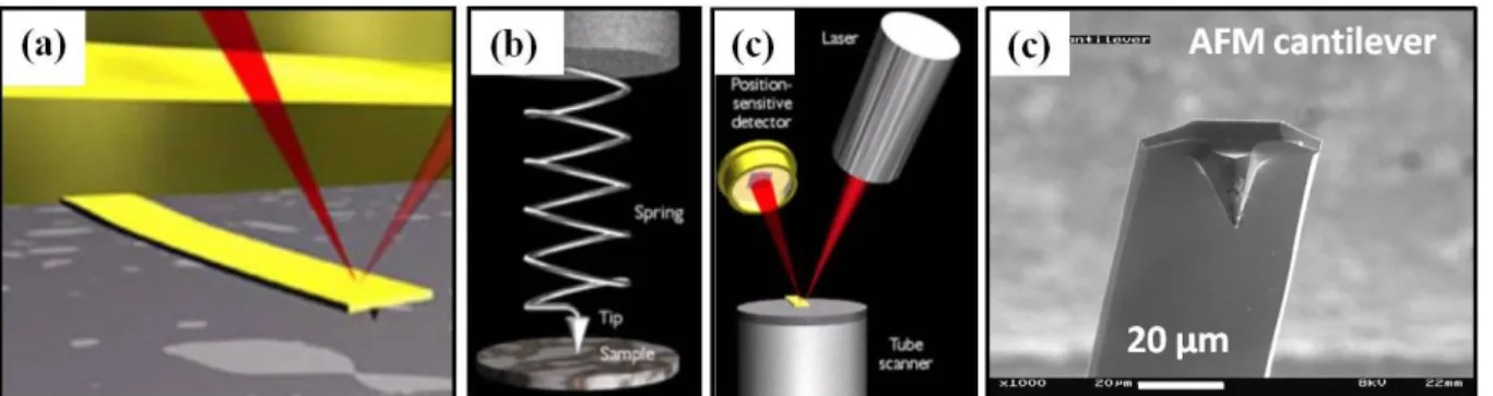
Fig. 3.2.3 Concept of AFM and the optical lever: (a) a cantilever touching a sample (b) illustration of the meaning of "spring constant" as applied to cantilevers (c) the optical
lever (d) AFM cantilever image. ... 26
Fig. 3.2.4. The photograph and the schematic setup of DCXRD system. ... 27
Fig. 3.2.5. Bragg diffraction from (a) a symmetric plane and (b) an asymmetric plane. ... 28
Fig. 3.2.6. Geometry for x-ray rocking curve. The angle movement for the detector is twice that of the sample. ... 29
Fig. 3.2.7. Schematic diagram of a SEM. ... 30
Fig. 3.2.8. Ray diagram showing two basic operations of TEM. ... 31
Fig. 3.2.9. The schematic of electroluminescence setup. ... 32
Fig. 3.2.10. The photograph of electroluminescence measure system. ... 32
Fig. 4.2.1. Schematic of InGaN/AlGaN and InGaN/InAlGaN MQWs structures. ... 43
Fig. 4.2.2. Schematic of AlGaN and InAlGaN single heteroepitaxial layers. ... 44
Fig. 4.3.1. Room-temperature PL spectra of AlGaN and InAlGaN single heteroepitaxial layers. ... 45
Fig. 4.3.2. Shows surface morphology AFM over 5×5 μm2 of AlGaN (RMS:0.813 nm) and InAlGaN (RMS:0.595 nm) layer with thickness about 50 nm. ... 46
Fig. 4.3.3. Surface morphology of top-view AFM images over 5×5 μm2 of LT GaN, AlGaN, and InAlGaN layer. ... 47
Fig. 4.3.4. HRXRD (ω-2θ) curves in the (a) (004) and (b) (105) reflections of GaN, AlGaN, and InAlGaN single heteroepitaxial layers. ... 48
Fig. 4.3.5. HRXRD (105) RSM of GaN, AlGaN, and InAlGaN single heteroepitaxial layers. ... 48
Fig. 4.3.6. HRXRD (ω-2θ) curves in the (002) reflections of InGaN/AlGaN and InGaN/InAlGaN MQWs. ... 49
Fig. 4.3.7. Cross-sectional TEM images of (a) InGaN/AlGaN and (b) InGaN/InAlGaN MQWs. The diffraction condition is g0002. ... 49 Fig. 4.3.8. Cross-sectional TEM images of (a) InGaN/AlGaN and (b) InGaN/InAlGaN LED structures. Inset in Fig. 4.3.8 shows ternary and quaternary MQWs structure. ... 50 Fig. 4.4.1. (a) 2-inch near-UV LED epi-wafer under 100 mA, (b) the mesa-type near-UV chip and (c) chip image under 350 mA driving current. ... 51 Fig. 4.4.2. L-I-V curves of the LEDs with AlGaN (dash) and InAlGaN (solid) barrier. ... 51 Fig. 4.4.3. Normalized Efficiency curves of experimental (open circles) and simulated (solid lines). ... 52 Fig. 4.4.4. EL spectra for InGaN/AlGaN and InGAN/InAlGaN MQWs under (a) (b) CW current and (c) (d) pulsed current with 100 μs and a 1 % duty cycle. ... 53 Fig. 4.4.5. EL peak energy of the (top) near-UV and (bottom) green LEDs as a function of the CW and pulsed modes. ... 54 Fig. 4.4.6. EL spectra for the near-UV LED (top) with increasing (a) CW current and (b) pulsed current, and green LED (bottom) with increasing (c) CW current and (d) pulsed current with a duty cycle of 1 %. ... 55 Fig. 4.4.7. Bandgap (dashed-line contours) and total polarization charge (solid-line contours) of AlGaInN as a function of Al and In compositions. ... 56 Fig. 4.4.8. Schematic of band diagram and band-offset ratio from 6:4 (InGaN/AlGaN) to 7:3 (InGaN/InAlGaN). ... 57 Fig. 4.4.9. Normalized IQE of InGaN/InAlGaN near-UV LED with different band-offset ratio from 5:5, 6:4 to 7:3. Inset in Fig. 4.4.9 shows the L-I curves of the InGaN/InAlGaN LEDs. ... 57 Fig. 4.4.10. Simulation results of normalized IQE under different carrier mobility. ... 58 Fig. 4.5.1. Distribution of (a) Electron (b) Hole concentrations, and (c) Radiative recombination
rates concentrations of the LEDs with AlGaN and InAlGaN barrier under a high forward current den sity of 100 A/cm2. ... 59 Fig. 5.2.1. Schematic of (a) ud-GaN/Sapphire (b) top-down etching (c) lateral etching (d) HIP GaN/air/Sapphire structure. ... 62 Fig. 5.2.2. The process flowchart for fabrication of GaN-based vertical LED: (a) GaN on Sapphire; (b) The HIP GaN/air/Sapphire structure; (c) GaN-based LED structure on HIP GaN/air/Sapphire template; (d)Wafer bonding process; (e) Remove sapphire substrate by mechanical lift-off during cooling process. ... 64 Fig. 5.3.1. (a) The tilted SEM image of the HIP structure; (b) SEM image of the etched GaN surface. Inset in Fig. 5.3.1 show the zoom in view images of the HIP structure. ... 65 Fig. 5.3.2. Cross-sectional SEM images of (a) The regrowth HIP GaN/air/Sapphire interface; (b) Zoom in view of the interface. ... 66 Fig. 5.3.3. Cross-sectional TEM images of (a) GaN-based LED structure grown on HIP GaN/air/Sapphire template (b) The regrowth HIP GaN/air/Sapphire boundary. The diffraction condition is g0002. ... 67 Fig. 5.3.4. Cross-sectional SEM image of the vertical LED structure after mechanical lift-off GaN LED/Silicon from sapphire substrate. Inset in Fig. 5.3.4 shows top-view SEM image of the HIP surface morphology after lift-off from sapphire substrate. ... 68 Fig. 5.3.5. Room temperature Raman spectrum of GaN epilayer regrowth on HIP structure and mechanical lift-off by HIP structure. ... 69 Fig. 5.3.6. (a) EL spectra of Ref-LED and V-LED in normal direction at 20mA. (b) The peak wavelength shift of the LEDs. Inset in Fig. 5.3.6 (a) shows the schematic of the Ref-LED and V-LED. ... 70 Fig. 5.3.7. L-I-V characteristics of the two fabricated LEDs. ... 71 Fig. 5.3.8. (a) An image of V-LED/Si wafer after lift-off process from sapphire substrate. (b)
The light emitting image of near-UV V-LED is observed at 20 mA operating currents. (c) OM image of 380×380 μm2 V-LED chip at a 1 mA current injection. ... 71 Fig. 5.4.1. Schematic of mechanical lift-off process. ... 73 Fig. 6.1. Schematic structures of 365 nm UV LEDs with (a) Al0.15Ga0.85N barrier and (b)
In0.02Al0.18Ga0.8N barrier. ... 77
Fig. 6.2. The process flowchart for fabrication of V-LEDs by using the porous SiO2/GaN
List of Tables
Table 3.1. Material parameters of the binary semiconductors GaN, AlN, and InN at room
temperature. ... 34
Table 3.2. Bandgap energy of GaN, AlN and InN related-temperature parameters. ... 36
Table 3.3. Mobility parameters of GaN, AlN and InN. ... 40
Table 4.1. Growth parameters of the InAlGaN, AlGaN, and InGaN MQWs ... 43
Table 4.2. Simulation parameters in band-offset ratio and carrier mobility. ... 59
Chapter 1
IntroductionIntroduction
1.1 Wide Bandgap Ⅲ-Nitride Materials
In recent decades, the III-Nitrides materials (InN, GaN, and AlN related alloys) become an interesting class of wide bandgap materials and play an important role in semiconductor devices [1-6]. Wide direct bandgap nitride materials have attracted great attention due to their promising potential for the applications of optoelectronic devices such as backlight of display, competing storage technologies, automobiles, general lighting, and biotechnology [7-10]. The bandgap of III-nitrides material cover a very wide range, from 0.7 eV for InN, to 3.4 eV for GaN, and to 6.1 eV for AlN [11, 12], which represents the emission wavelength from infrared (IR) region to deep ultraviolet (UV). Fig. 1.1.1 shows the bandgaps of various alloys of III-Nitrides [13].
Fig. 1.1.1. Bandgap energy versus lattice constant of III-V nitride semiconductors at room temperature.
The wide bandgap implies the large band off-set in hetero-structure or multi quantum well (MQW) could be achieved in this material system. The large band off-set is very useful
to confine carrier for the high-speed and high power electronic devices and light emitting devices [14]. Although wurtzite nitride compounds have some unique properties such as piezoelectric field and spontaneous polarization which is unfavorable to the efficiency of optoelectronic devices, the material system still is a very strong candidate for the future optoelectronic applications due to their superior material properties.
1.2 GaN-based Near-Ultraviolet Light-Emitting Diodes (Near-UV LEDs)
Pioneering work of Pankove, Akasaki, Amano, Schubert, and Nakamura has led to the development of bright green and blue LEDs based on nitride semiconductors in the recent decade. The first blue light-emitting diode (LED) using III-nitrides materials was fabricated by J. I. Pankove et al. [15] in 1972. Since that, related research about GaN-based material is going on continually. However, progresses have been limited because of highly background
n-type concentration resulting from the native defects commonly thought to be nitrogen
vacancies and residual impurities such as silicon and oxygen acted as an efficient donor, poorly conducting p-type GaN, and the lack of appropriate substrates for epitaxial growth. Until late 1980s, I. Akasaki and H. Amano et al. discovered a very useful method of an AlN buffer layer and developed low-energy electron beam interaction (LEEBI) techniques to obtain a better quality GaN film and conductive p-type GaN layer [16-18]. The quality of GaN thin film grown by atmospheric pressure metal-organic vapor phase epitaxial (AP-MOVPE) using AlN buffer layers is shown to be excellent in terms of morphological, crystalline, and optical properties. Using AlN buffer layers, GaN thin films with optically flat surfaces free from cracks are successfully grown. The narrower x‐ray rocking curve of GaN film with AlN buffer layer from the (0006) plane is shown in Fig. 1.2.1 [16]. In 1989, I. Akasaki et al. put a sample of GaN:Mg in a scanning electron microscope (SEM) with an optical window through which they could see the blue cathodoluminescence. As shown in Fig.
1.2.1, they noticed that the intensity of luminescence kept getting stronger the longer they scanned. When the brightness seemed to saturate they took the sample out and measured the Hall effect. To their great surprise and to the world’s astonishment, the previously insulating sample had become conducting p-type [17].
Fig. 1.2.1. X-ray rocking curve for (0006) diffraction from GaN grown at 970 °C with the AlN buffer layer. Dotted line shows data obtained by HVPE.
Fig. 1.2.2. Photoluminescence spectra of GaN:Mg (b) before and (a) after the electron beam treatment. The ratio of the two peaks is 100.
Until 1991, S. Nakamura developed a new buffer layer for high quality GaN growth by MOVPE. Strenuous efforts were made to optimize growth conditions by introducing suitable
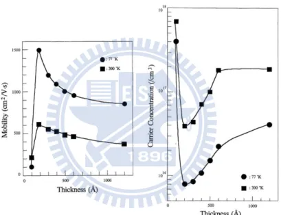
buffer layers (between the sapphire substrate and the active GaN) of GaN grown at low temperatures (~ 500 °C) and by adjusting flow rates and temperatures with the object of reducing n-type background doping levels and increasing Hall mobility. The optimum thickness of the GaN buffer layer was around 200 Å . Fig. 1.2.3 shows the Hall mobility and carrier concentration measured at 77 K and 300 K as a function of the thickness of the GaN buffer layer.This eventually proved successful high Hall mobility values of 600 cm2/V.s at 300 K and background levels below 1017 cm-3 were achieved, followed by the important breakthrough of p-type doping at the end of the 1980s [19].
Fig. 1.2.3. The Hall mobility and carrier concentration measured at 77 K and 300 K as a function of the thickness of the GaN buffer layer.
These discoveries initiated a new strong interest in this research field. Finally, the first GaN-based blue LED constructed of a real p-n junction was achieved, which had greatly improved in the device performance. However, the acceptor concentration of p-type GaN is still too low such that the application of these materials is still unreliable. After that, in 1992, S. Nakamura et al. made the definitive experiment that showed by thermal annealing in nitrogen ambient that above 700°C the passivating H was dissociated from Mg, rendering
temperatures. H could be reintroduced by heating in NH3 making GaN:Mg insulating again
[20]. Afterward Nakamura and Mukai et al. [21] succeeded in growing high-quality InGaN films that emitted strong band-to-band emission from green to UV region by changing the indium content of InGaN with a two-flow MOCVD method. Nowadays, most of III-Nitride based LEDs use InGaN as active layer instead of GaN, since adding a small amount of indium into the GaN is very important to obtain a strong band-to-band emission at RT.
Fig. 1.2.4. Resistivity of GaN:Mg after annealing at various temperatures.
The most spectacular application and the first commercial GaN product is the LED. In 1997, Nakamura et al. have produced the brightest LEDs using GaN p-n junctions that include a Zn-doped well as shown in Fig. 1.2.5 [22]. The purpose of the well is to confine the carriers in a small volume, and the purpose of the Zn is to introduce an efficient blue or green luminescent center [23].
Further development of the AlN, AlGaN and AlInGaN materials resulted in an appearance of ultraviolet (UV) LEDs which represent the next frontier in solid-state optoelectronics with a large potential in biological, medical and environmental instrumentation, resin curing, photo-catalyst for disinfection and deodorization, UV light source [24], and there have been interests in solid-state lighting by using near-UV LEDs light
for the phosphor-converting source [25, 26].
Fig. 1.2.5. Structure of III-Nitride light emitting diodes (LEDs).
Near-UV LED has some unique advantages, such as safer operation with very low heat generation, low electricity consumption, without UVB and UVC dangerous wavelengths, no warm-up time, instant turn on/off, lower operating voltage, compact and scalable design for ease of integration, much longer service life, and environmentally friendly with no ozone emissions or dangerous mercury. Fig. 1.2.6 shows extensively applications of Near-UV LEDs.
Fig. 1.2.6. Applications of Near-UV LEDs.
A great progress in solid-state sources of GaN-based p-n junction UV light was achieved by Akasaki et al. in 1992 [4]. Present UV LEDs are based on heterostructures developed
[29], and quaternary AlInGaN [30, 31]. There are two main issues of GaN-based UV LED: the chips must feature band diagrams structure that assists high efficiency of carrier injection into the active layer, the internal quantum efficiency (IQE) should be maximized by enhancing radiative recombination and restraining the nonradiative recombination, and light generated in active layer must be efficiently extracted from the chip. Certainly, reduction of the dislocation density, solving self-absorption of GaN, and preventing cracking of epitaxial layers mismatched to the substrate is one of the most important issues.
Most of GaN-based UV LEDs are grown on sapphire substrate, which has a 16 % lattice mismatch with GaN. This disadvantage is being bypassed through dislocation reducing by epitaxial lateral overgrowth (ELO) and by using superlattices, strain-compensating layers and quaternary AlInGaN alloys. To increase the IQE of UV LEDs, optimization of quantum well structures is necessary through selecting composition and doping profiles of the well, barrier and p-type layers, shaping of the interfaces between well and barrier, and engineering of the built-in electric field to avoid the quantum-confined Stark effect (QCSE). In addition, basic investigation for unveiling the routes of nonradiative recombination in AlGaN alloys with high molar fraction of aluminum is needed. To overcome the high resistivity of p-AlGaN, novel doping approaches including piezoelectric and super-lattice doping, graded composition, and co-doping of magnesium (Mg) and indium (In) are being developed.
First commercial 375 nm LEDs were fabricated by Nichia in 1998 [28]. Typically, these devices feature 1.5~2 mW light output power and are available with the out-coupling optics for narrow-angle (20 °) and wide-angle (110 °) far-field radiation pattern. Cree fabricated the first near-UV LED for use in the illumination market in 2001. The InGaN based devices were grown on SiC substrate, and the light output power was about 12 mW with the wavelength between 395~405 nm. These near-UV LEDs have a geometrically enhanced vertical chip structure to maximize light extraction efficiency and require only a single Au-wire bond
connection with the device.
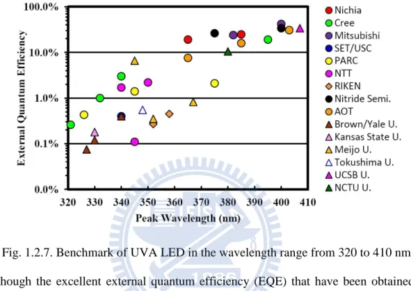
Shown in Fig. 1.2.7 is the benchmark of history development of GaN-based UVA LED in the wavelength range from 320 to 410 nm [32]. From the benchmark, it can be deliberated that the UV LED has an energetic development after 1998.
Fig. 1.2.7. Benchmark of UVA LED in the wavelength range from 320 to 410 nm. Although the excellent external quantum efficiency (EQE) that have been obtained by many groups for LEDs in the near UV range, the EQE of InGaN-based UV LEDs with emission wavelength shorter than 365 nm is at least one order of magnitude below the best devices in the near-UV wavelength range about 400 nm. There are multiple causes that currently limit the EQE of GaN-based UV LEDs. For example, with decreasing wavelengths, the light output power is dropping and challenges in growing high quality nitride heterostructures with a high aluminum (Al) molar fraction are becoming more difficult [30]. The solutions to device problems lie in using better substrates (ex: AlN substrates in non-polar orientations, and patterned sapphire substrate), using better epitaxial growth techniques (ex: ELO), improving device design (ex: vertical chip and flip chip) and using better contact technology.
1.3 Content of Dissertation
In this study, there are several major contributions for fabricating high efficient near-UV LEDs such as (a) inserting a quaternary material of InAlGaN layers for quantum barrier (b) fabricating a high quality GaN-based V-LED structure by using mechanical lift-off (MLO) technology, will review as below:
(a) InAlGaN barrier near-UV LED
One of the major problems of efficiency decay in near-UV is the lack of an excellent distribution of carriers in multi-quantum-well (MQW) active region. To solve this issue, we prepare a 50-nm InAlGaN and AlGaN single heteroepitaxial layers, and the quaternary structure of InGaN/InAlGaN and ternary structure of InGaN/AlGaN MQW grown on n-AlGaN/ud-GaN/Sapphire substrate. Several properties of optical, surface morphology and MQWs structure have been measured by photoluminescence (PL), atomic force microscopy (AFM), high-resolution double crystal x-ray diffraction (DCXRD) and transmission electron microscopy (TEM), respectively. Electroluminescence (EL) results indicate that the light output power of quaternary LEDs can be enhanced by 25 % and 55 % at 350 mA and 1000mA, respectively. Finally, the optical and electrical properties of quaternary InGaN/InAlGaN and conventional InGaN/AlGaN MQW LEDs are numerically calculated using the APSYS simulation software [33]. Simulation results show that InGaN-based UV LEDs with quaternary InAlGaN barrier exhibit higher radiative recombination rate and low efficiency droop. The details of the physical origin in efficiency droop are investigated in chapter 4.
(b) Mechanical lift-off (MLO) technology
Sapphire is the most commonly used substrate because of its relative low cost during the last decade of years, but it also limits the devices performance due to its poor electrical and thermal conductivity. In order to improve the device performance, it is necessary to develop a
method to separate device from sapphire substrate. The techniques of laser lift-off (LLO) [34, 35] and chemical lift-off (CLO) [36-38] have been adopted to fabricate the freestanding GaN membrane and the vertical LEDs (V-LEDs) for the purpose of high performance devices. However, the LLO process may induce some possible damages under high temperature in the GaN/sapphire interface. And even though the CLO can prevent the GaN layer from the laser damage during the laser lift-off process, but it also makes another chemical etching damages and reduce the crystal quality. Hence, we study the fabrication of mechanical lift-off (MLO) for high quality GaN-based V-LEDs with Hexagonal Inversed Pyramid (HIP) structures. Scanning electron microscopy (SEM) and transmission electron microscopy (TEM) images reveal the clear GaN/sapphire interface before and after the re-growth process. Raman spectrum shows the residual stress of the LED can also be considerably reduced while introducing the HIP structure to the GaN/sapphire interface. Finally, the optical and electrical properties of high efficient near-UV V-LEDs have been measured and the physical mechanisms of lift-off process are also carefully investigated in chapter 5.
Chapter 2
Properties of InGaN-based Near-UV LEDsProperties of InGaN-based Near-UV LEDs
For many biological, medical and environmental instrumentation, resin curing, and photo-catalyst applications as mentioned previously, LEDs operating in the UV region of the spectrum are more and more interested. However, any LED-emitting radiation above the energy of violet light is accessible by low indium-nitride (InN) molar fraction indium-gallium -nitride (InGaN) active layer, some amount of In seems to be a requisite for localization-enhanced radiative emission. Besides, with decreasing wavelengths, the efficiency is dropping and challenges in growing high quality nitride-based barrier with a high aluminum (Al) molar fraction are becoming more difficult. Nevertheless, LEDs based on InGaN quantum well active layers just below the violet wavelengths have been developed and the range of wavelength between 380 nm and 410 nm is denominated near-UV LEDs.
The properties of physical and material such as InGaN active layer, GaN self-absorption, indium-tin-oxide (ITO) film serving as a transparent contact layer (TCL), definition of efficiencies, and the origin of efficiency droop of InGaN-based near-UV LEDs will be described in detail in this section.
2.1 Structure of InGaN-based Near-UV LEDs
2.1.1 Epitaxy Structure of InGaN-based Near-UV LED
Currently, the most commonly used method to achieve GaN-based LEDs is using by metal-organic chemical vapor deposition (MOCVD) system. A detailed introduction of MOCVD technology will be described in Chap. 3.
For the growth of InGaN-based LEDs, trimethyl gallium (TMGa), trimethyl indium (TMIn), trimethyl aluminum (TMAl), and ammonia (NH3) were used as the source precursors
for Ga, In, Al, and N, respectively. Silane (SiH4) and bis-cyclopentadienyl magnesium
(Cp2Mg) were used as n-type and p-type dopants. The conventional structure of InGaN-based
near-UV LEDs consists of a low-temperature (500C) 30-nm-thick GaN nucleation layer, a 1-m-thick un-doped GaN buffer layer, a 3-m-thick Si-doped GaN cladding laye (or Si-doped AlGaN cladding layer), a InGaN active layer (or 10 periods of InGaN/AlGaN MQWs active region), a 20-nm-thick Mg-doped AlGaN cladding layers serving as a electron blocking layer (EBL), and a 100-nm-thick Mg-doped GaN contact layer.
The varieties possessing of GaN-based active layer such as InGaN single-quantum-well (SQW), InGaN/GaN double heterostructure (DH) [40], GaN/AlGaN [27], InGaN/AlGaN [28], AlGaN/AlGaN [29], and quaternary AlInGaN [30, 31] multi-quantum-well (MQWs) were developed in the past two decades.
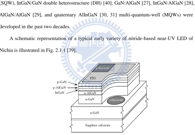
A schematic representation of a typical early variety of nitride-based near-UV LED of Nichia is illustrated in Fig. 2.1.1 [39].
Fig. 2.1.1. Schematic of nitride-based near-UV LED of Nichia.
Some amount of In is necessary for localization-enhanced radiative intensity. Because InGaN lends itself to composition fluctuations or clustering and thus reduced adverse effects of nonradiative recombination, the emission intensity drops as the InN mole fraction is reduced near the GaN end of the ternary. As mentioned of the benchmark of UVA LED in Fig.
1.2.7, the external quantum efficiency (EQE) as functions of the wavelength. By reducing the InN mole fraction in InGaN active layer, the wavelength of operation can be shifted to the shorter spectrum. When the InN mole fraction is lower, as indicated above, the emission intensity degrades extremely. Shorter wavelength of near-UV and UV LED need larger bandgap energy to prevent the electron overflow, and the adequate barrier height whether in quantum barrier or p-type cladding layer depends on the wavelength desired.
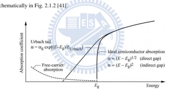
It is worth mentioning for the issue of GaN self-absorption in near-UV LED. To obtain high light-extraction efficiency and avoid absorption of light, all semiconductor layers other than the active region should have a bandgap energy larger than the photon energy. The absorption coefficient v.s. energy of an idealized semiconductor and a real semiconductor is shown schematically in Fig. 2.1.2 [41].
Fig. 2.1.2. Absorption coefficient of a semiconductor with bandgap Eg versus energy. In this absorption tail, called the Urbach tail, the absorption coefficient v.s. energy is given by:
where αg is the experimentally determined absorption coefficient at the bandgap energy and
EUrbach is the characteristic energy (here called the Urbach energy), which determines how
rapidly the absorption coefficient decreases for below bandgap energies. Urbach (1953) measured the absorption tail for different temperatures and showed that the Urbach energy is
approximately kT, the thermal energy.
The "Urbach tail" dominates absorption near but below the bandgap energy, and absorption further below the bandgap is dominated by free-carrier absorption as shown in Fig. 2.1.2.
The energy of photons emitted from a semiconductor with energy gap Eg is given by the bandgap energy, i.e.
where h is the Planck's constant, ν the frequency, c the speed of light in a vacuum, and λ the wavelength of emission light.
Therefore, the wavelength of near-UV range from 410 nm to 380 nm can be converted to the energy gap by 3.02 eV and 3.26 eV, respectively. Obviously, the bandgap energy of n-GaN (3.39~3.418 eV) [42, 43] or p-GaN (3.27~2.88 eV) [44-49] is near or below the emission light of near-UV range, thus the absorption effect is more significant as the wavelength become shorter. For this reason, the applicable way to avoid self-absorption is to reduce the thickness of each layer which the bandgap energy near or below the emission light such as n-type and p-type material and replace the n-GaN by n-AlGaN under layer.
2.1.2 Chip Structure of Near-UV LEDs
There are three types of typical chip design for GaN-based near-UV LEDs: mesa-type chip, flip-chip, and vertical-chip, respectively. Because of the advantages of simple process and low cost, the most commonly used for near-UV LEDs is sapphire-based mesa-type chip. The schematic representation of a typical mesa-type chip is illustrated in Fig. 2.1.3. The light generated in the active InGaN MQWs traverses the chip without any appreciable absorption, as the entire chip is transparent to the radiation wavelength except for the self-absorption in
spreading resistance in the top p-GaN layer is large. To overcome this problem, a transparent top contact such as indium-tin-oxide (ITO) became popular.
Fig. 2.1.3. Schematic of GaN-based mesa-type chip.
The LED with a transparent and conductive large-area contact made of ITO connects to the top p-type GaN layer for better optical and electrical transportation. In the wavelength around 400 nm, the transmittance through 3000 Å -thick of ITO layer is about 90 %. The method naturally keeps the lower contact resistance to the p-type GaN layer, by virtue of increased area of contact, and reduces current crowding and associated ill effects.
Flip-chip is also used in near-UV LED for high power applications. The schematic representation of a typical flip-chip is illustrated in Fig. 2.1.4 [50]. The devices were subsequently fabricated by etching square mesa structures by inductively coupled plasma (ICP), reactive ion etching (RIE) or chemically assisted ion beam etching (CAIBE) with the length of the sides ranging from 100 to 900 μm. Ti/Al metal contacts were then deposited on the exposed n-type AlGaN current spreading layer for the lateral electrical connection and Ni/Au contacts on the p-type GaN layer for hole injection [32]. The flip-chip mount method is used in which the p-side is mounted face down on a metallic mirror and the light is collected from the n-side layer and the sapphire substrate. Therefore, the method achieves the higher light extraction efficiency (LEE) and better thermal dissipation, but this design is still unable to resolve the problem of current crowding under high current density driving.
Fig. 2.1.4. Schematic of a UV LED flip-chip mounted onto a heat sink substrate. To achieve higher light excitation and light output performance, the LED must be driven under high current density. For better thermal management, a heat sink substrate is necessary to avoid early saturation in the LED output power due to the inherent joule heating and current crowding issues. The schematic representation of a typical vertical chip is illustrated in Fig. 2.1.5.
The structure of vertical-type chip can be achieved by laser lift-off (LLO) or chemical lift-off (CLO) techniques for the purpose of high performance optoelectronic devices. Many advantages of vertical-type structure such as higher thermal conductivity for the use of metal alloyed substrate, higher reflectivity of metallic mirror between p-GaN/substrate interface, without absorption issue from TCL for the p-side down design, vertical current path for uniform current spreading, and without current crowding issue between two electrodes.
2.2 The Physical Definition of Efficiencies
LED is a classical semiconductor diode that emits spontaneous radiation under suitable forward bias condition. Under forward bias conditions, both electrons from n-type and holes from p-type semiconductor inject into active region and then recombine in the smaller bandgap active region, and accompany by the emission of a photon (radiatively) or non-radiatively. These two recombination pathways can be considered as parallel processes occurring across the bandgap of the active region material, as illustrated in Fig. 2.2.1.
Fig. 2.2.1. Illustration of radiative and non-radiative transition in a semiconductor. If the radiative lifetime is denoted as τr and the non-radiative lifetime is denoted as τnr,
then the total probability of recombination in active region is given by the sum of the radiative and non-radiative probabilities:
The relative probability of radiative recombination is given by the radiative probability over the total probability of recombination. Therefore, the internal quantum efficiency (IQE) can be expressed in terms of the radiative and non-radiative lifetimes.
where the IQE is denoted as ηIQE. In other words, the definition of ηIQE is the ratio of the
injected into the p-n junction LED. From the concept of electrical excitation mechanism, the internal quantum efficiency is defined as:
where Pint is the optical power emitted from the active region, and I is the injection current.
In an ideal LED, all photons produced in the active region will emit into free space. However, in a real device, a part of photons will not emit into the free space because of absorption and total internal reflection (TIR) issues.
The extraction efficiency can be a severe limitation for high performance LEDs. It is quite difficult to increase the extraction efficiency without resorting to high sophisticated and costly device processes. The light extraction efficiency (LEE) is defined as:
where the LEE is denoted as ηLEE, and P is the optical power emitted into free space.
Considering the refractive indices of GaN (n = 2.5) and air (n = 1), for the light escape cone is about 23.6 % due to the critical angle. Assuming that light emitted from sidewalls and backside is neglected, one expects that approximately only 4.18 % of the internal light can be extracted from a surface of the device.
Finally, the external quantum efficiency (EQE) can be defined as:
where the EQE is denoted as ηEQE. From the above equation, we can know that the EQE
depend on IQE and LEE. Therefore, the improvement of IQE and LEE play a very important role for fabricating a high performance LED.
Finally, the wall-plug efficiency (WPE) of LEDs can be described by the following relationship: where the WPE is denoted as ηWPE, Pout the light output power, I the drive current, V the
operating voltage, and ħω the photon energy [51].
2.3 The Basic Concept of Efficiency Droop
Although significant progress in GaN-based LEDs has been made in recent decades, higher efficiencies and light output power are necessary for using in general lighting and high power light source market. However, the efficiency of LED generally is highest at a low current density around a few milliampere (mA). Besides, the efficiency decreases gradually as the injection current increases [52-56]. As shown in Fig. 2.3.1, the normalized efficiency as a function of the current density shows efficiency droop of GaN-based LEDs. The efficiency reaches its peak at current densities as low as 10 A/cm2 and monotonically decreases with further increase in current.
This well-known phenomenon of efficiency droop must be solved for devices operating at high current density. A solution to the efficiency droop issue has not yet been provided, and different explanations were proposed extensively. However, the physical origin of efficiency droop is not well understood.
Currently, dislocations have been shown to reduce the overall efficiency but not affect the efficiency droop [57]. The major cause of efficiency droop in GaN-based LED is still a huge controversy in last decade of years, and several possible mechanisms of droop including carrier overflow [58-62], non-uniform distribution of holes [63, 64], Auger recombination and scattering [65-68], carrier delocalization [69-71], junction heating [72] have been proposed, but the genesis of the efficiency droop is still the topic of an active debate.
Although Auger recombination was proposed for the efficiency droop [61], the Auger losses in such a wide bandgap semiconductor are expected to be very small [73], which has also been verified that the direct Auger losses are negligible in InGaN quantum wells by using fully microscopic many body models [74].
Chapter 3
Experimental Instruments and Physical ModelsExperimental Instruments and Physical Models
Experimental instruments employed in this research contain metal-organic chemical vapor deposition (MOCVD), photoluminescence (PL), atomic force microscopy (AFM), raman system, high-resolution double crystal x-ray diffraction (DCXRD), scanning electron microscopy (SEM), cathodoluminescence (CL), transmission electron microscopy (TEM), and electroluminescence (EL). Furthermore, the physical models, bandgap energy, band offset ratio, and carrier transport mechanism will be described in detail in this chapter.
3.1 Metal-organic Chemical Vapor Deposition System (MOCVD)
Metal-organic chemical vapor deposition (MOCVD) is a growth technique that includes a dynamic flow in which gaseous reactants flow over a heated substrate and react chemically in the surface to form a semiconductor layer [75]. It has been widely used in modern semiconductor industry, which provide a way to grow high-quality semiconductor films and sharp interface. Its potentials have also been proven by producing high quality epitaxial structures with excellent surface morphology and a precise control for layer thickness and uniformity. Several epitaxial crystal growth technologies for an impressive array of commercial devices are also carried out by MOCVD, such as lasers, LEDs, photo-cathodes, high electron mobility transistor (HEMT), photo-detectors, and solar cells.
MOCVD growth is facilitated by introducing group III precursors (Al, Ga, and In) and NH3 with carrier gases into a reactor under suitable total flow rate, rotation speed, growth
temperature, and growth pressure. As shown in Fig. 3.1.1, a typical MOCVD system consists of four major parts: (a) Control panel (b) Gas delivery system (c) Reactor chamber (d) Heating system (e) Gas exhaust system.
Fig. 3.1.1. III-N based MOCVD system (Nippon Sanso SR-4000).
The precursors TriMethyl-Gallium (TMGa), TriMethyl-Aluminum (TMAl), and TriMethyl-Indium (TMIn) react with ammonia (NH3) on the heated substrate surface to form
semiconductor layers. Additional sources such as hydrogen (H2), nitrogen (N2), silane (SiH4),
disilane (Si2H6), and Bis(cyclopentadienyl) magnesium (Cp2Mg) sources are needed. The
precursor molecules NH3 and TMAl, TMGa and TMIn are fed in separately into the reactor
chamber as shown in Fig. 3.1.2.
Fig. 3.1.2. Scheme of metal-organic chemical vapor deposition (MOCVD) growth. The basic MOCVD reaction describing the GaN deposition process is:
However, the details of the reaction are not well known because the intermediate reactions are so complex. Several types of MOCVD system are being developed for the mass production of GaN-based materials and devices. Both atmospheric-pressure and low-pressure
systems are being produced by the major MOCVD equipment manufacturer such as Aixtron, Tomas Swan (merged by Aixtron in 1999), Veeco, Emcore (merged by Veeco in 2003), and Nippon Sanso.
3.2 Materials and devices analysis
3.2.1 Photoluminescence (PL)
Photoluminescence is a process in which a substance absorbs photons (electromagnetic radiation) and then re-radiates photons. It has been widely used as a measurement method to detect the optical properties of the semiconductor materials because of its non-destructive characteristics. PL can reveal the band structure and the carrier transportation behaviors in a semiconductor material. Moreover, the bandgap, doping type, composition, lifetime, etc. of the nano-scale semiconductor material can be shown in the PL spectrum. So the PL could be a judgment of the material quality, semiconductor characteristic, and be a key instrument of the development for nano-technology.
In general, PL system use a laser as a light source, and the laser light source used to excite carriers should have larger energy bandgap than the semiconductor materials. When the laser light is absorbed within the semiconductors, it would excite the carriers from the valence band to the conduction band. During the process it produces the electrons in the conduction band and the holes in the valence band as shown in Fig. 3.2.1. In a direct gap material, the conduction band minimum and the valence band maximum occur at the same k values. Direct gap semiconductor materials are excellent light emitters and their optical properties can be analyzed by using this technique.
Fig. 3.2.1. Schematic band diagrams for the photoluminescence processes in a direct gap material.
The PL spectroscopy is the optical measurement to examine the quality and optical characteristic of material. First, when we analysis an unknown compound semiconductor, we can use PL measurement to know the band gap of the unknown material. Second, the intensity of PL signal is contributed to the amount of radiative recombination in the materials. Therefore, PL measurement can be used to understand the material quality and the recombination mechanisms of the materials.
The schematic setup of our PL system is shown in Fig. 3.2.2. The pumping source was a multi-mode and non-polarized Helium-Cadmium laser operated on 325 nm with 35 mW. After reflecting by three mirrors, the laser light was focused by a lens which focal length was 5 cm, to 0.1 mm in diameter and the luminescence signal was collected by some lens. The probed light was dispersed by 0.32 monochromator (Jobin-Yvon Triax-320) with 1800, 1200, and 300 grooves/mm grating and the maximum width if the entrance slit was 1 mm. In order to prevent the laser coupling with the PL spectrum, we used the long pass filter in front of the entrance slit.
Fig. 3.2.2. The schematic of experimental Photoluminescence setup.
3.2.2 Atomic Force Microscopy (AFM)
Atomic force microscopy (AFM) or scanning force microscopy (SFM) is a very high-resolution type of scanning probe microscopy, with demonstrated resolution on the order of fractions of a nanometer, more than 1000 times better than the optical diffraction limit of optical microscope system. The AFM or SFM was invented in 1986 by Binnig, Quate and Gerber. Like all other scanning probe microscopes, the AFM utilizes a sharp probe moving over the surface of a sample in a raster scan.
The AFM consists of a cantilever with a sharp tip (probe) at its end that is used to scan the sample surface. Fig. 3.2.3 shows the concept of AFM and the optical lever. As shown in Fig. 3.2.3 (a), the probe is a tip on the end of a cantilever which bends in response to the force between the tip and the sample. The small probe-sample separation (on the order of the instrument's resolution) makes it possible to take measurements over a small area. To acquire an image the microscope raster-scans the probe over the sample while measuring the local property in question. The resulting image resembles an image on a television screen in that
both consist of many rows or lines of information placed one above the other. Unlike traditional microscopes, scanned-probe systems do not use lenses, so the size of the probe rather than diffraction effect generally limits their resolution. The cantilever is typically silicon or silicon nitride with a tip radius of curvature on the order of nanometers as shown in Fig. 3.2.3 (d).
Fig. 3.2.3 Concept of AFM and the optical lever: (a) a cantilever touching a sample (b) illustration of the meaning of "spring constant" as applied to cantilevers (c) the optical lever
(d) AFM cantilever image.
3.2.3 Double Crystal X-ray Diffraction (DCXRD)
X-rays are a form of electromagnetic radiation with a wavelength range from 10 to 0.01 nanometers. The wavelength must be smaller that the atomic spacing of the material being analyzed. The x-rays are created from an electron beam striking a target. The beam should be monochromatic with a very small divergence obtained by collimation.
Fig. 3.2.4. shows photograph and the schematic setup of DCXRD system (Bede D1, UK, using Cu Kα1 λ = 1.54056 Å). X-rays scatter from atoms by different degrees which are dependent on the atom type. However for a good quality x-ray beam incident on a well ordered crystalline material (such as a single crystal semiconductor) the scattered x-rays interfere with each other and result in a diffracted beam leaving the material.
Fig. 3.2.4. The photograph and the schematic setup of DCXRD system.
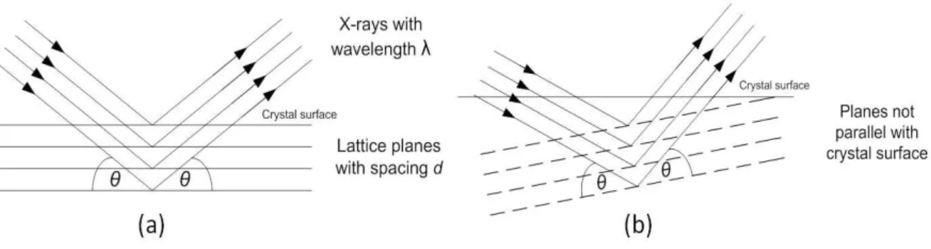
This type of diffraction is caused by parallel planes of atoms, in the same way that light may be diffracted by a diffraction grating. For any given values of x-ray wavelength and angle of incidence of the x-ray beam only one set of parallel planes will cause diffraction. This is formalized in Bragg’s Law which states:
Where n is an integer value, 1, 2, 3 etc., λ is the wavelength of the x-ray beam, d is the lattice constant, the spacing between adjacent parallel planes and θ is the angle to the normal of the plane at which the x-ray beam is incident. The diffracted beam leaves the crystal plane at the same angle from the plane’s normal as the incident beam, but in the opposite direction, as can be seen in the Fig. 3.2.5 (a). It shows a ‘symmetric reflection’, so called because the
diffracting plane is parallel to the surface of the crystal. This is the case for diffraction from the 004 plane of a standard orientation (surface is the 001 plane) semiconductor wafer.
Fig. 3.2.5 (b) shows an ‘asymmetric reflection’, in which the diffracting plane is not parallel to the surface of the crystal.
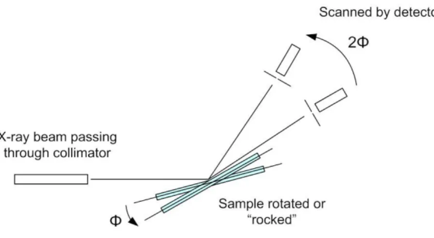
If the same x-ray source and beam conditioner are used then it can be safely assumed that ‘λ’ does not change. Each family of planes within a crystal has a characteristic and unique ‘d’ value. It is not possible for diffraction to occur from more than one plane if a single good quality (low divergence and approximately monochromatic) x-ray beam is used. Because of this, knowing the orientation of a wafer allows any plane to be chosen as the diffracting plane. When an x-ray beam is fired at a crystal, and the crystal is then rotated through a small angle as observed in Fig. 3.2.6, the diffracted intensity should sharply increase from zero and then sharply decrease to zero, as the x-ray beam–crystal angle passes through the Bragg angle, ‘θ’. This is commonly displayed on a ‘rocking curve’, which plots the angle at which the crystal is tilted against the intensity of x-rays from the crystal.
Bragg’s Law above suggests that for a perfect single crystal and a good quality x-ray beam, one sharp peak should be seen only. Even with a perfect beam of x-rays, rocking curves for more complicated structures, such as the multiple quantum well laser will show multiple peaks.
Fig. 3.2.6. Geometry for x-ray rocking curve. The angle movement for the detector is twice that of the sample.
3.2.4 Scanning Electron Microscopy (SEM)
The electron microscope uses electromagnetic lenses to focus the beam to produce an image. However, SEM and TEM differ in the way images are produced and magnified. SEM is used to view the surface or near surface of a sample, whereas TEM provides information of the internal structure of thin specimens. The scanning electron microscope as the name suggests scans across the specimen by the scan coils.
As the sample is scanned by the electron beam as shown in Fig. 3.2.7, it emits electrons and electromagnetic radiation. A detector counts the low energy secondary electrons (< 50 eV) or other radiation emitted. The image is produced by two dimensional intensity distributions by scanning a cathode ray tube (CRT) spot onto a screen and modulating the brightness by the amplified current from the detector. Three dimensional samples change the way electrons are emitted and results in the appearance of a three dimensional image. Therefore, resolutions less than 1 nm can be achieved by using SEM system.
Fig. 3.2.7. Schematic diagram of a SEM.
3.2.5 Transmission Electron Microscopy (TEM)
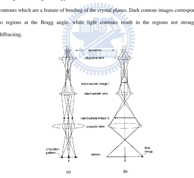
TEM is a method of imaging where a beam of electrons are directed through a an ultra thin sample after which they are scattered into discrete diffracted beams. The diffracted electron beams are then focused in the back focal plane of the objective lens. TEM may have two modes. When operated in diffraction mode, the diffraction lens is focused on the back focal plane to produce a diffraction pattern. For the imaging mode, the diffraction lens is focused on the first image plane to produce a magnified image. In addition, the beam may be allowed to pass through the sample to obtain a bright-field image however the diffracted beams produce a dark-field image.
The ray diagram (Fig. 3.2.8) shows (a) imaging projecting a diffraction pattern and (b) projection of an image onto a viewing screen. The interaction of the electron beam with crystalline material tends to be by diffraction. The orientation of the planes of atoms in the crystal to the electron beam changes the intensity of diffraction. TEM equipment often uses a goniometer to allow the sample to be tilted to a range of angles to obtain specific diffraction
conditions. Diffracted electrons are also selected using different apertures. The intensity of diffraction is a maximum at the Bragg angle, although a variation of diffraction intensity occurs with deviation from the Bragg angle. This also depends on the thickness of the specimen. The thinner the crystal sample, the further the crystal may deviate from the Bragg condition.
When crystal planes are almost parallel to the electron beam they are close to fulfilling Bragg’s Law. The majority of electrons are diffracted when the electron beam strikes one set of lattice planes exactly at their Bragg angle and only a few will pass through the sample undeviated. If the planes are exactly at the Bragg condition, strong diffraction will occur and the bright field image will appear dark. This variation with diffraction is shown with bend contours which are a feature of bending of the crystal planes. Dark contour images correspond to regions at the Bragg angle, while light contours result in the regions not strongly diffracting.
3.2.6 Electroluminescence (EL)
Electroluminescence (EL) is an optical and electrical phenomenon in which a material emits light in response to the passage of an electric current or under an electric field. Fig. 3.2.9 shows the schematic of electroluminescence measurement systems. A set of instruments including CW current source Kiethley 238, a microscope to observe the patterned electrode of sample surface, three axial stages for probe and fiber to detected the light output, and then the light detected by a 0.32 m monochromator (Jobin-Yvon Triax-320) with 1800, 1200, and 300 grooves/mm grating and the maximum width if the entrance slit was 1 mm. Fig. 3.2.10 shows the photograph of electroluminescence measure system.
Fig. 3.2.9. The schematic of electroluminescence setup.
3.3 Advanced Physical Models of Semiconductor Devices (APSYS)
To explore the physical origin and theoretically in this study, the numerical simulation software of APSYS (Advanced Physical Models of Semiconductor Devices) was used to predict and optimize our LEDs design in each layer. It is based on 2D/3D finite element analysis of electrical, optical and thermal properties of compound semiconductor devices. Emphasis is placed on band structure engineering and quantum mechanical effects. Inclusion of various optical modules also makes this simulation package attractive for applications involving photosensitive or light emitting devices. The APSYS simulator solves the Poisson’s equation, the current continuity equations, the carrier transport equations, the quantum mechanical wave equation, and the heat transfer equations, via self-consistent manner. Built-in polarization induced by spontaneous and piezoelectric polarization is considered at hetero-interfaces of nitride related devices. We put commonly accepted physical parameters to perform the simulations. Usually, for performing a simulation, the used material parameters had been set as default data from former research results. However, we also can modify and update these values to be similar to real device. Therefore, setting suitable parameters for simulation is an important point.
3.3.1 Theoretical Model
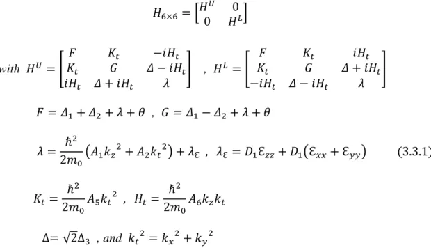
The physical model of the InGaN MQWs is considered in such a way that the conduction bands are assumed to be decoupled from valence subbands and have isotropic parabolic bands due to the larger bandgap of nitride semiconductor and the valence band structures, which includes the coupling of the heavy-hole (HH), the light-hole (LH), and the spin-orbit split-off bands, are calculated by the 6×6 Hamiltonian with envelop function approximation. By using the basis transformation, the 6×6 Hamiltonian can be transformed into a block-diagonalized Hamiltonian [76],