行政院國家科學委員會專題研究計畫 成果報告
軟性半導體與光電關鍵整合技術研究(3/3)
研究成果報告(完整版)
計 畫 類 別 : 整合型 計 畫 編 號 : NSC 98-2218-E-009-001- 執 行 期 間 : 98 年 08 月 01 日至 99 年 10 月 31 日 執 行 單 位 : 國立交通大學應用化學系(所) 計 畫 主 持 人 : 張豐志 共 同 主 持 人 : 柯富祥、林俊宏、張雯惠 處 理 方 式 : 本計畫可公開查詢中 華 民 國 100 年 04 月 20 日
1
國科會工程處軟性電子跨領域專案
全程期末成果報告
I、 計畫基本資料
計 畫 名 稱 軟性半導體與光電關鍵整合技術研究 計 畫 編 號NSC- 96-2218- E-009-008, NSC- 97-2218- E-009-002
NSC- 98-2218- E-009-001
執 行 期 間 民國 96 年 8 月 1 日~民國 99 年 10 月 31 日 計畫總主持人 張豐志 教授 交通大學應用化學系 共同主持人 柯富祥 教授 交通大學奈米科技研究所 共同主持人 張雯惠 副教授 中山醫學大學應用化學系 共同主持人 林俊宏 助理教授 成功大學光電科技研究所 年度 經費(元) 參與人力 教授 博士後 研究 博士生 碩士生 大學部 專題生 96 5,143,000 4 0 4 6 0 97 5,143,000 4 0 4 6 0 98 5,143,000 4 0 4 6 0II、 成果統計
年度 期刊論文(篇) 會議論文(篇) ACI (篇) SCI (篇) EI (篇) 國內 國外 國內 國外 96 5 4 6 5 97 5 4 6 5 98 5 5 5 5 合計 15 13 17 15 5 篇重要論文說明 Fabrication of patterned superhydrophobic polybenzoxazine hybrid surfaces, Langmuir 25, 3359–3362 (2009) 在任意基板上合成並控制高分子 材料之親水及疏水特性
A new organic/inorganic electroluminescent material with a silsesquioxane core, Acta Materialia 57, 1938–1946 (2009) 合成具備熱穩定 性及高抗氧化能力之發光複合材料、製作出具有高強度與光色澤度之 PLED 元件
2
Patterned Poly(2-hydroxyethyl methacrylate) Brushes on Silicon Surfaces Behave as “Tentacles” To Capture Ferritin from Aqueous Solution, ACS Appl. Mater. Interfaces, 1, 1525–1532 (2009) 在任意基板上合成並藉
由親疏水溶劑操控高分子材料之表面形態
Improved reliability from a plasma-assisted metal-insulator-metal capacitor comprising a high-k HfO2 film on a flexible polyimide substrate,
Phys. Chem. Chem. Phys., 12, 2582–2589 (2010) 利用溶膠凝膠旋轉塗佈技
術製造下世代軟性電容元件之高介電層並可撓曲 10 萬次
Highly reliable, nanoscale and eco-friendly thin film composite materials as a dielectric layer for next generation flexible MIM capacitors, ChemSusChem, accepted for publication (2010) 製備出具有共聚高分子與
小分子互拌的環境相容之軟性元件的低介電層技術 年度 專利申請數 已獲專利數 專利應用 國內 國外 國內 國外 國內 國外 96 1 97 98 合計 5 項重要專利或技術(授權)說明 「金屬-半導體-金屬光電檢測器應用於整合式生物晶片」:本申請中 發明專利係利用成本低廉、製程簡單、而且快速的金屬-半導體-金屬光電 偵測器,將具有催化效果之生物分子直接固定化到偵測器表面,由冷光分 子反應以獲取光電流訊號,可以使金屬-半導體-金屬光電偵測器直接收集 冷光並轉換成電流訊號,可以避免訊號之漏失並降低外在環境之污染。本 元件可以以軟性物質覆蓋而形成一種具軟性可撓曲的特性。 年度 技術授權 (件) 產學合作 (件) 學術活動 (場、人數) 96 1 1、150 97 2 1、150 98 2 合計 5 2、300
3
III、 計畫成果概述
A1.基礎材料
高分子材料
Tuning the Surface Free Energy of Polybenzoxazine Thin Films
(在任意基板上合成並控制高分子材料之親水及疏水特性, The Journal of
Physical Chemistry C 112, 16189-16191 (2008))
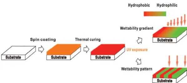
A novel approach to manipulate the surface free energy and wettability on polybenzoxazine thin films can be achieved simply by varying the time of thermal treatment or UV exposure. A fraction of the intramolecular hydrogen bonding of the as-cured sample will convert into intermolecular hydrogen bonding upon thermal treatment or UV exposure and, thus, results in an increase in the hydrophilicity and wettability. The surface free energies obtained from two-liquid geometric method indicate that the polar forces between the PBZ thin film and the testing liquids increased substantially after UV exposure, in addition, the ESCA results reveal that the atomic fraction of oxygen, an indication of the degree of photo-oxidation of the surface, increased dramatically after UV exposure, concluding that the UV exposure led to oxidation and cleavage of the isopropylidene linkages of PBZ, forming 2,6-disubstituted benzoquinone units which would influence the fraction of the intramolecular hydrogen bonding within PBZ and result in the wettability gradients on the surface of PBZ.
Fig. 1. Fabrication of wettability gradients and wettability patterns on B-ala PBZ films.
4
IV、 成果自評
此項目應包含下述內容:
(1)成果報告內容與原計畫相符程度
(2)預期目標達成情況
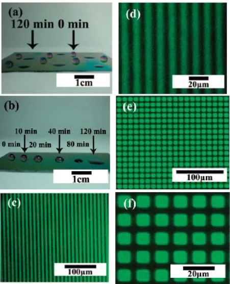
Fig. 2. (a) Wettabilty pattern, (b) wettablity gradient, and (c-f) periodic arrangement of CdTe colloidal nanocrystals on B-ala PBZ films.
5
高分子材料
Efficient Polymer Light-Emitting Diodes Using a New Hole Transport Layer
(高效能之電動傳輸材料並有效大幅提升 PLED 元件效率, submitted to Adv.
Mat.)
More recently, research on organic materials possessing low hole-injection and high conductivity has focused on poly(3,4-ethylenedioxythiophene)–poly- (styrenesulfonate) (PEDOT-PSS) because of its planar structure which leads to high electron delocalization along the chain. PEDOT has relatively high conductivity (10-3–10-5 S/cm) and good transparency affecting carrier injection and device performance directly. It has been applied in various electronic products such as light-emitting diodes, photovoltaic devices, and organic thin-film transistors.
In our recent study, a new series of hole transport materials (HTMs) containing neither ion nor hydrophilic functionality have been developed. We first discover an extremely high hole transport ability through assembling these materials into double-layer device. The resulting device performance is “several times” higher than that of PEDOT (Table 1). Through detailed studies of polymer interactions and morphologies, we understand why these materials possess such unique hole transport property. In this report, now we would like to further extend our studies for applications in areas such as high performance light-emitting diode (LED), organic solar cell and flexible device.
Table 1:electroluminescence performances of HTM and PEDOT films based devices
Samples Max Peak (nm)
Max Luminance (cd/m2)
Max Luminance efficiency (cd/A)
Max Power efficiency (lm/w)
HTM 518 6283 1.487 0.46
PEDOT 509* <100 0.14 0.08
Samples Max Peak (nm)
Max Luminance (cd/m2)
Max Luminance efficiency (cd/A)
Max Power efficiency (lm/w)
HTM 518 6283 1.487 0.46
PEDOT 509* <100 0.14 0.08
6
無機與有機混成材料
A New Organic/Inorganic Electroluminescent Material with a Silsesquioxane Core
(合成具備熱穩定性及高抗氧化能力之發光複合材料, Acta Materialia 57,
1938-1946 (2009))
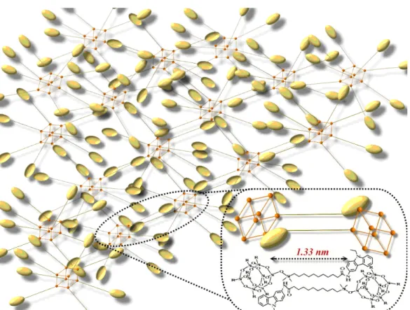
This research describes a new polyhedral oligomeric silsesquioxane (POSS)-based blue-light electroluminescent nanoparticle, octakis[N-(9-ethyl-9H-carbazol-3-yl) undecanamide-11-dimethylsiloxy] silsesquioxane (POSS-C11-Cz), which contains eight carbazole chromophore arms, synthesized through the hydrosilation reaction of octakis(dimethylsiloxy)silsesquioxane with the terminal olefin Cz-C11ene. POSS-C11-Cz exhibits good thermal and electrochemical stabilities and good film-forming properties. The optical and photoluminescence spectra of POSS-C11-Cz in solution and in the solid state indicate a reduction in the degrees of aggregation and excimer formation because interchain interactions were prohibited by the bulky POSS core.
Fig. 1. Graphical representation of the well-ordered dispersive structure formed from POSS-C11-Cz in bulk state.
7
300
400
500
600
700
0.0
0.2
0.4
0.6
0.8
1.0
(4) (4) (3) (2) (1)Normalized Intensity
Wavelength (nm)
POSS-C11-Cz (UV)
PACz (UV)
POSS-C11-Cz (PL)
PACz (PL)
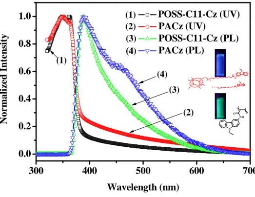
(4) (3) (2) (1)Fig. 2. UV–vis absorption and PL emission spectra of POSS-C11-Cz and PACz in the solid state.
-600 -300 0 300 600 900 1200 (5) (4) (3) (2) (1) (5) Potential(mv) vs. Ag/Ag+ (0.01 M) Ferrocene Scan 1 Scan 2 Scan 3 Scan 4 (4) (3) (2) (1)
Fig. 3. Cyclic voltammagrams of POSS-C11-Cz.
N N H O O SiO Si O S i O Si O Si O Si O Si O Si O O O O R O R R R R R R Si R = N N H O O Si N NH O n
8
無機與有機混成材料
Patterned Poly(2-hydroxyethyl methacrylate) Brushes on Silicon Surfaces Behave as “Tentacles” To Capture Ferritin from Aqueous Solution
(在任意基板上合成並藉由親疏水溶劑操控高分子材料之表面形態, ACS
Appl. Mater. Interfaces, 1, 1525–1532 (2009))
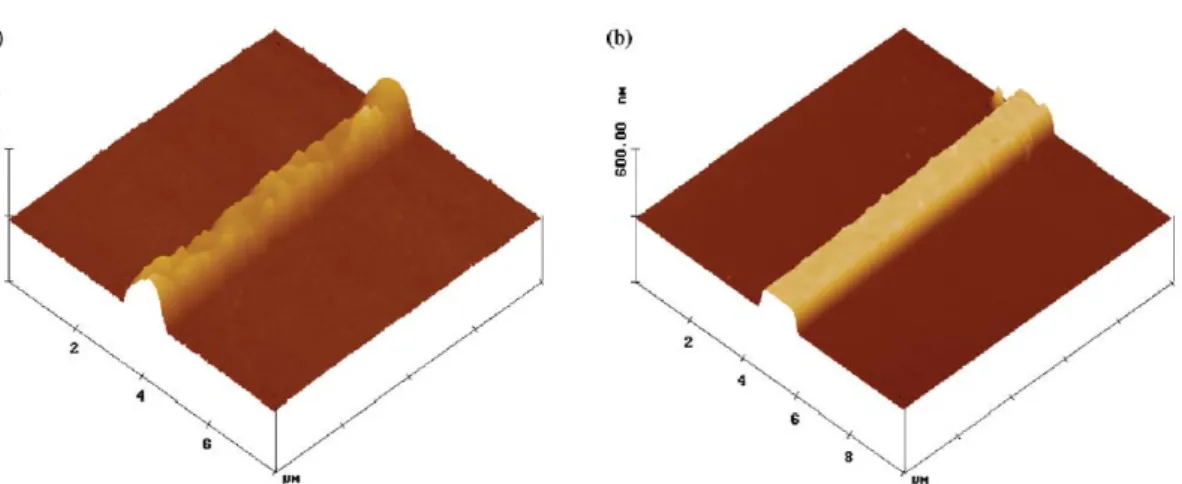
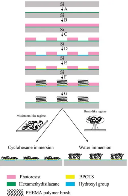
We have used a very large scale integration process to generate well-defined patterns of polymerized 2-hydroxyethyl methacrylate (HEMA) on patterned Si(100) surfaces. An atom transfer radical polymerization initiator covalently bonded to the patterned surface was employed for the graft polymerization of HEMA to prepare the poly(2-hydroxyethyl methacrylate) (PHEMA) brushes. After immersing wafers presenting lines of these polymers in water and cyclohexane, we observed brush- and mushroomlike regions, respectively, for the PHEMA brushes, with various pattern resolutions. The PHEMA brushes behaved as “tentacles” that captured ferritin complexes from aqueous solution through entanglement between the brushes and the ferritin proteins, whose ferritins were trapped due to the collapsing of the PHEMA. Using high-resolution scanning electron microscopy, we observed patterned ferritin iron cores on the Si surface after thermal removal of the patterned PHEMA brushes and ferritin protein sheaths.
Fig 1. AFM images of PHEMA brushes grafted from 750 nm trenches for 24 h and then immersed in (a) water and (b) cyclohexane.
9
Fig 2. Schematic representation of the process used to fabricate surfaces chemically nanopatterned with PHEMA brushes: (A) Si wafer treated with HMDS in a thermal evaporator; (B) photoresist spincoated onto the Si surface presenting Si(CH3)3 groups; (C) advanced lithography used to pattern the photoresist with arrays of trenches and contact holes on the surface; (D) oxygen plasma etching used to chemically modify the exposed regions presenting Si(OCH3)3 groups and to convert the topographic photoresist pattern into a chemical surface pattern; (E) initiator (BPOTS) selectively assembled onto bare regions of the Si surface; (F) sample grafting via surfaceinitiated ATRP of HEMA from the functionalized areas of the patterned SAM; (G) photoresist removed through treatment with solvent.
10
A2.軟性元件
發光元件
Photoluminescence and PLED Manufactured Through POSS-C11-Cz/ Polyfluorene Blend
(製作出具有高強度與光色澤度之 PLED 元件, Acta Materialia 57, 1938-1946
(2009))
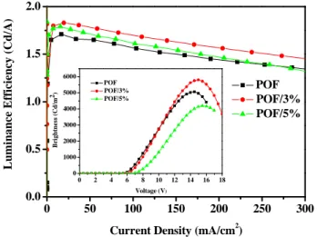
From optical and electroluminescence measurements, we found that the attachment to the POSS cage suppressed the aggregation and enhanced the color stability of 3,9-carbazole units both in solution and in the solid state. POSS-C11-Cz also behaves as an effective dopant that enhances energy transfer from itself to POF. In addition, POSS-C11-Cz improves the quantum efficiency and color stability of POF because its presence reduces the degree of aggregation and the formation of keto defects. A POSS-C11-Cz (3 wt%)/POF (97 wt%)-based device exhibited higher maximum brightness and luminance efficiency than did the non-blended POF-based device. Devices were fabricated in the configuration ITO/poly(3,4-ethylene dioxythiophene) (PEDOT, 35 nm)/polymer (ca. 60 nm)/1,3,5-tris(N-phenylbenzimidazol-2-yl)benzene (TPBI, 30 nm)/LiF (150 nm )/Al (100 nm). We assembled the device through sequential coating of PEDOT (to improve the hole injection), POSS-C11-Cz (emissive layer), TPBI (electro-transport material), LiF (electrode), and Al layers onto ITO (transparent anode). Interestingly, the maximum brightness of the EL obtained from a POSS-C11-Cz (3 wt%)/PACz (97 wt%) blend was twice that of the PACz-based device, and the turn-on voltage was reduced from 10.5 to 7.5 V. Thus, a small amount POSS-C11-Cz acted as an effective dopant to transfer energy to PACz; therefore, POSS-C11-Cz appears to have potential for use in improving the quantum efficiency and color stability of polyfluorenes through blending. The PL spectra (figure 2) reveal that the green emission peak at 530 nm of the POSS-C11-Cz (3%)/POF (97%) blend in the solid state had a lower intensity than that of the POF polymer itself. The PL stability of this blend is similar to that of other polyfluorene derivatives, indicating that incorporation of POSS-C11-Cz into POF polymer reduces the extent of both aggregation and keto defects of the POF. In addition, the incorporation of POSS-C11-Cz did not appreciably change the EL and quantum efficiencies of the POF. However, the POSS-C11-Cz (3 wt%)/POF (97 wt%)-based device exhibited higher maximum brightness and luminance efficiency than did the POF-based device because of the doping effect of POSS-C11-Cz (figure 3), which enhanced energy transfer efficiency from the carbazole chromophore groups on POSS-C11-Cz to POF and suppressed the
11
aggregation of POF. We are continuing to study these systems to elucidate the factors affecting their morphological control in bulk state and to develop materials that devices can be fabricated on flexible substrates.
Fig. 1. The triple-layer devices based on this complex present the following configurations: ITO/PEDOT, /polymer/TPBI,/Al .
400 450 500 550 600 0.0 0.2 0.4 0.6 0.8 1.0 POF-pristine POF-annealed POF/3%-annealed (3) (3) (2) (2) (1) (1) PL Int ensit y (a .u. ) Wavelength (nm) (2) (3)
Fig. 2. PL spectra of spin-coated films of pristine POF, annealed POF and annealed POF/3% POSS-C11-Cz; annealing conditions: 200oC, 5 h.
0 50 100 150 200 250 300 0.0 0.5 1.0 1.5 2.0 0 2 4 6 8 10 12 14 16 18 0 1000 2000 3000 4000 5000 6000 POF POF/3% POF/5% B ri g ht nes s (C d/ m 2) Voltage (V) POF POF/3% POF/5% L u m inance E fficiency (Cd/A)
Current Density (mA/cm2)
Fig. 3. EL spectra and voltage – external quantum efficiency characteristics of POSS-C11-Cz/POF-based devices.
12
軟性高介電元件
Improved reliability from a plasma-assisted metal-insulator-metal capacitor comprising a high-k HfO2 film on a flexible polyimide substrate
(利用溶膠凝膠旋轉塗佈技術製造下世代軟性電容元件之高介電層並可撓曲
10 萬次, Phys. Chem. Chem. Phys. 12, 2582-2589 (2010))
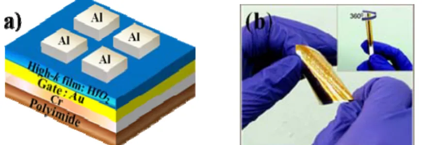
Plastic circuits have received growing interest because they combine plastic substrates with new classes of organic materials using low-cost fabrication approaches, such as inkjet printing and liquid film casting. They are considered to be a key emerging technology for this century with their potential as an ultralow-cost and light-weight alternative to Si wafers. In some instances, they are compatible with continuous, high-speed reel-to-reel fabrication, high mechanical flexibility, transparent to visible/UV radiation, and can allow the circuit board to conform to a desired shape or flex during its use. Subsequently, plastic circuits appear to be a foundation for future electronic devices, such as electronic papers, wearable sensors, low-cost smart cards, radio frequency identification tags, and flexible arrays of plastic microphones. Recently, in terms of their superior bending, it was found that flexible organic transistors can perform better than flexible inorganic transistors. Reliability stress testing is very important method for analyzing the bending and stretching properties of flexible devices designed for such applications as accurate sensors for hydrogen or for integration into artificial muscles or biological tissues. We have used a sol–gel spin-coating process to fabricate a new metal–insulator–metal (MIM) capacitor in Fig. 1 comprising a 10 nm–thick high-k thin dielectric HfO2 film on a flexible polyimide (PI) substrate.
The surface morphology of this HfO2 film was investigated using atomic force
microscopy and scanning electron microscopy, which confirmed that continuous and crack-free film growth had occurred on the film surface. After oxygen (O2)
plasma pretreatment and subsequent annealing at 250°C, the film on the PI substrate exhibited a low leakage current density of 3.64x10⁻⁹ A cm–2 at 5 V and a maximum capacitance density of 10.35 fF µm–2 at 1 MHz. The as-deposited sol– gel film was completely oxidized when employing O2 plasma at a relatively low
temperature (ca. 250 ° C), thereby enhancing the electrical performance. We employed X-ray photoelectron spectroscopy (XPS) at both high and low resolution to examine the chemical composition of the film subjected to various treatment conditions. The shift of the XPS peaks towards higher binding energy, revealed that O2 plasma treatment was the most effective process for the complete
oxidation of hafnium atoms at low temperature. A study of the insulator properties indicated the excellent bendability of our MIM capacitor; the flexible PI substrate
13
could be bent up to 105 times in Fig. 2 and folded-to near 360° without any deterioration in its electrical performance.
Fig. 1. (a) Schematic representation of an MIM capacitor featuring a high-k HfO2
thin film on a PI substrate; (b) Photograph of our MIM capacitor on the flexible ultra-thin PI substrate; inset: unlimited bend test up to an angle of 360° angle.
Fig. 2. Leakage current density plotted as a function of the electric field, measured at both negative and positive biased voltages, for the OPT/A-treated flexible MIM capacitor after being subjected to repeated bendings for various times.
14
軟性低介電元件
Highly reliable, nanoscale and eco-friendly thin film composite materials as a dielectric layer for next generation flexible MIM capacitors
(製備出具有共聚高分子與小分子互拌的環境相容之軟性元件的低介電層技
術, ChemSusChem, accepted for publication (2010))
Currently, there has been increasing demands on reducing the feature size in microelectronic products and more interested in the development of electronic circuits on flexible substrates to meet the growing worldwide demand for low processing temperature, low-cost fabrication, large-area, and lightweight devices. In addition, ultra-low dielectric constant (k) materials are crucial to minimizing resistive-capacitive (RC) delay, power consumption, and cross-talk noise. And most of the organic-organic nanocomposites are known as low-k dielectric material. Therefore, organic/polymer and organic-polymer nanocomposite materials have attracted a lot of attention for building large-area and mechanically flexible electronic devices. These materials are also widely pursued because they offer numerous advantages in terms of ease of processing, good compatibility with a variety of substrates, and great opportunity for structural modifications. Apart from above mention there is also a strong desire to develop new large-scale materials that can meet the growing demand for miniaturization, high-speed performance, and flexibility for microelectronic devices. And the next generation of intermetal dielectric (IMD) materials for microelectronic devices must have an ultra-low-k of less than 2.0 to meet the National Technology Roadmap for Semiconductors. New organic-organic nanoscale composite thin film (NCTF) dielectric in Figs. 1 and 2 has been synthesized via solution deposition of 1-bromoadamantane and triblock copolymer (Pluronic P123, BASF, EO20-PO70-EO20), where the precursor solution has been achieved with organic
additives. We have used a sol-gel process to make metal-insulator-metal capacitor comprising a nanoscale (10 nm-thick) thin-film on flexible polyimide (PI) substrate at room temperature. Scanning electron microscope and atomic force microscope revealed that the deposited NCTFs were crack-free, uniform, high resistance to moisture absorption and well adhered on the Au/Cr/PI. The electrical properties of 1-bromoadamantane-P123 NCTF were characterized by dielectric constant, capacitance and leakage current measurements. The 1-bromoadamantane-P123 NCTF on the PI substrate showed low leakage current density of 5.5×10⁻¹¹ A cm-2 and good capacitance of 2.4 fF at 1 MHz. In addition, the calculated dielectric constant of 1-bromoadamantane-P123 NCTF is 1.9, making them suitable candidates for use in future flexible electronic devices as a stable intermetal dielectric. The electrical insulating properties in Fig. 3 of
15
1-bromoadamantane-P123 NCTF have been improved due to the optimized dipole moments of van der Waals interaction.
Fig. 1. Schematic view of the 1-bromoadamantane-P123 nanoscale composite thin film based MIM capacitor and (B) photograph of the flexible MIM capacitor fabricated on PI substrate; shows the capacitor bent by hand.
Fig. 2. Schematic of synthesis of 1-bromoadamantane and P123 composite precursor employed for fabrication of organic-organic nanoscale composite thin film dielectric.
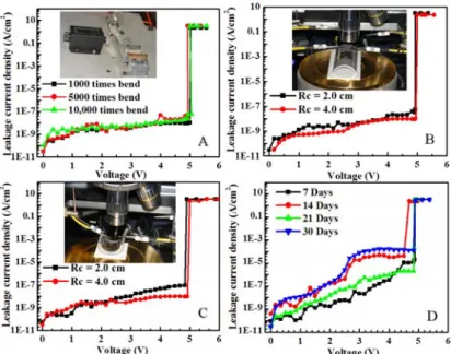
Fig. 6. J-V plots for MIM structure fabricated with 1-bromoadamantane-P123 nanoscale composite thin film: (A) bending test, the inset shows a photograph of homemade bending system (B) convex shape test, the inset shows a photograph of convex setting (C) concave shape test, the inset shows a photograph of concave setting and (D) day-dependent leakage current density.
16 (3)研究成果之學術或應用價值
本計畫針對軟性基礎材料與軟性元件進行深入的研究,並已經有具有深度的學術 成果發表在著名的期刊上,包括Journal of Physical Chemistry C (IF 4.224)、Acta Materialia (IF 3.76)、ACS Appl. Mater. Interfaces (ACS)、Phys. Chem. Chem. Phys. (IF 4.116)、ChemSusChem (IF 4.767)等。藉由各種量測技術,這些材料的物性與 化性均被仔細的探討,此外所製得的軟性元件的光電特性,亦深入的研究。最有 價值的是我們自行發展出撓曲設備,此設備應用到開發的軟性元件之可靠度性能 評估。我們所製得的軟性電子元件均可以任意角度撓曲或折疊,且其可以在經過 1萬次以上的撓曲,並不會有明顯電性的變化,表示我們針對軟性元件所發展的 溶膠凝膠旋轉塗佈技術是具有相當優秀的產業應用性,這些產業包括電子業、顯 視器業、服裝業等,目前我們正準備進行專利的申請。 (4)學術期刊或專利之發表情形 如前所述,我們已經將研究成果發表在著名的期刊上,包括Journal of Physical Chemistry C (IF 4.224)、Acta Materialia (IF 3.76)、ACS Appl. Mater. Interfaces (ACS)、Phys. Chem. Chem. Phys. (IF 4.116)、ChemSusChem (IF 4.767)等。目前我 們也研續先前程果進行軟性電晶體研發,由於研發團隊對軟性電子元件研發已經 有三年的經驗,預期我們後續會有更多的學術期刊與專利發表。本計畫總主持人 執行計畫的第二年亦獲得國家講座,因為係第二次獲得,因此目前為教育部終身 國家講座。
國科會補助計畫衍生研發成果推廣資料表
日期:2011/04/20國科會補助計畫
計畫名稱: 軟性半導體與光電關鍵整合技術研究(3/3) 計畫主持人: 張豐志 計畫編號: 98-2218-E-009-001- 學門領域: 軟性電子跨領域專案計畫無研發成果推廣資料
98 年度專題研究計畫研究成果彙整表
計畫主持人:張豐志 計畫編號: 98-2218-E-009-001-計畫名稱:軟性半導體與光電關鍵整合技術研究(3/3) 量化 成果項目 實際已達成 數(被接受 或已發表) 預期總達成 數(含實際已 達成數) 本計畫實 際貢獻百 分比 單位 備 註 ( 質 化 說 明:如 數 個 計 畫 共 同 成 果、成 果 列 為 該 期 刊 之 封 面 故 事 ... 等) 期刊論文 0 0 100% 研究報告/技術報告 0 0 100% 研討會論文 13 13 100% 篇 論文著作 專書 0 0 100% 申請中件數 0 0 100% 專利 已獲得件數 0 0 100% 件 件數 0 0 100% 件 技術移轉 權利金 0 0 100% 千元 碩士生 0 0 100% 博士生 0 0 100% 博士後研究員 0 0 100% 國內 參與計畫人力 (本國籍) 專任助理 0 0 100% 人次 期刊論文 15 15 100% 研究報告/技術報告 0 0 100% 研討會論文 17 17 100% 篇 論文著作 專書 0 0 100% 章/本 申請中件數 0 0 100% 專利 已獲得件數 0 0 100% 件 件數 0 0 100% 件 技術移轉 權利金 0 0 100% 千元 碩士生 6 6 100% 博士生 4 4 100% 博士後研究員 0 0 100% 國外 參與計畫人力 (外國籍) 專任助理 0 0 100% 人次其他成果