表面淺層蝕刻與鋅擴散的離子佈植型面射型雷射之製造與分析
75
0
0
全文
(2) 表面淺層蝕刻與鋅擴散的離子佈植型面射型雷射之製造與 分析 Fabrication and Analysis of Shallow Surface-Etched and Zinc-Diffused Ion-Implanted Vertical-Cavity Surface Emitting Lasers 研 究 生:林志明. Student:J. M. Lin. 指導教授:楊賜麟 博士. Advisor:Dr.S.L.Yang. 國 立 交 通 大 學 電 子 物 理 研 究 所 碩 士 論 文 A Thesis Submitted to Institute of Electrophysics College of Science National Chiao Tung University in Partial Fulfillment of the Requirements for the Degree of Master in ElectroPhysics July 2005 Hsinchu, Taiwan, Republic of China. 中華民國九十四年七月.
(3) 表面淺層蝕刻與鋅擴散的離子佈植型面射型雷射之製 造與分析. 研究生:林志明. 指導教授:楊賜麟 博士. 國立交通大學電子物理研究所. 摘要 本論文主要探討表面蝕刻及和鋅擴散對 850 nm 離子佈植面射 型雷射單模表現的影響。我們推導 Laguerre-Gaussian 模及線性偏振 模的光場強度於空間位置上的分佈,並分析溫度對橫模光點尺寸的影 響。在調節布拉格反射鏡的反射率方面,我們模擬計算表面蝕刻對原 有的 850 nm 分散型布拉格反射率的影響,得到 86 nm 的蝕刻深度, 可得到的最小反射率值 0.985,此結果與我們實作的實驗數據相吻 合。在布拉格反射鏡的表面進行鋅擴散的模擬計算上,我們得到隨著 擴散的時間增加,反射率下降且止帶間距縮小,而對原有反射率近乎 1.0 的 850 nm 分散型布拉格結構言,我們得到了在溫度 600 ℃ 下通 行 8 至 16 分鐘的鋅擴散時間可將分散型布拉格反射鏡的反射率改變. i.
(4) 為 0.95。將上述的兩種表面修正反射率的方法應用於製作單一橫模的 面射型雷射,由於離子佈植製程造成元件的串聯電阻過大,使得大部 分元件無法發光。其它發光的元件上我們量測 L-I 發現僅有發光二極 體的特性,導致此原因可能是因為表面反射率下降造成元件的臨界增 益增加,因此,不容易產生雷射光。. ii.
(5) Fabrication and Analysis of Shallow Surface-Etched and Zinc-Diffused Ion-Implanted Vertical-Cavity Surface Emitting Lasers. Student:J. M. Lin. Advisor:Dr. S. L. Yang. Institute of ElectroPhysics National Chaio Tung University. ABSTRACT. In this study, we fabricated and analyzed the 850 nm ion-implanted vertical-cavity surface emitting lasers (VCSELs) with shallow-etching and zinc-diffusion onto the surface distributed Bragg reflector (DBR). The Laguerre-Gaussian modes and linear polarization modes were applied for determining mode intensity distribution. The temperature effect on the mode spot size was evaluated. We calculated the reflectance of shallow-etched and zinc-diffused 850 nm DBR. We found that there is a local reflectance minimum of 0.985 with surface etching depth of 86 nm. This calculation is coincident to our experimental result. For the case of zinc diffusion, we found that the reflectance and stop band decrease with the diffusion time. The resultant DBR reflectance is about 0.95 with for the diffusion time of 8 ~ 16 minutes at 600 ℃. Due to an amorphous film formed over the DBR surface, the measured reflectance is much lower than the simulated result and is not. iii.
(6) comparable to the simulation result. We applied separately the shallow-etching and zinc-diffusion techniques to fabricate single mode 850 nm ion-implanted VCSELs. Due to a large series resistance of VCSELs resulted from the small ion-implanted aperture size, most devices cannot reach the threshold lasing condition. The measured relationship of light power to current indicates the characteristics of light emitting diodes. By adequately controlling the aperture sizes of ion-implantation and surface relief or zinc diffusion, the feasible single-mode VCSELs are suggested to be fabricated successfully.. iv.
(7) 誌 謝. 首先,我想感謝我的指導老師楊賜麟老師,張國彬學長及實驗室同學育 維、東昇、淼松、許國、仲安及學弟明曉,在實驗與課業上遇到困難時給予適時 的幫助。另外,特別感謝威凱科技的徐總經理、陳發慈副總經理、鄭如純副理和 威凱科技無塵室的學長吳燁峰和學姐徐靜寧以及其他幫助過我的工程師,特別是 吳燁峰學長在製程上給我寶貴的建議與製程的幫忙,更是讓我獲益匪淺。我也要 感謝光電所仿志僥學弟在光譜與電性上的量測給予及時的幫助以及電物所洪天 河先生在製程上的協助。 最後,我想感謝我的家人,在研究所兩年期間,他們不但是我精神上最大的 支柱,在物資方面也讓我無後顧之憂可以朝我的目標邁進。. v.
(8) Contents 中文摘要…………………………………………………………………i. 英文摘要……………………………………………………..…………iii. 誌謝………………………………………………………………………v Contents………………………………………………………………….vi Figure Contents………………………………………………………...viii Table Contents…………………………………………………………..xii Chapter 1. Introduction.....................................................................................1. 1-1. Introduction to VCSEL……………………….………………………………...1. 1-2. The structure of VCSEL……………………………………………………….1. 1-3. Outline of this thesis…………………………………………………………...4. Chapter 2 2-1. 2-2. The basic theory of VCSEL………………………………………….………..6 2-1-1. Threshold gain ……………………….……………………………..6. 2-1-2. Longitudinal Modes (Axial Modes) of a VCSEL…………………...8. 2-1-3. Rate equation………………………………………………………..9. Distribution Bragg reflector………………………………………………….10 2-2-1. 2-3. The Basic Principle and Simulation of VCSEL…………..6. Transmission Matrix method……………….………………………11. The transverse mode of VCSELs…………………………………………….18 2-3-1. Transverse optical confinement of VCSEL………………………...18. 2-3-2. Laguerre-Gaussian and Hermite-Gaussian Modes………………….20. vi.
(9) 2-3-3. Chapter3. Linearly Polarized Modes in a Dielectric Cylindrical Waveguide….28. Single Fundamental Mode VCSEL from the Surface Modified DBR reflectance……………………………………..33. 3-1. VCSELs of surface relief structure…………………………………………….33. 3-2. Surface Zinc diffusion to suppress high-order transverse modes……………...35 3-2-1. Temperature induces AlxGa1-xAs/GaAs inter-diffusion…………….36. 3-2-2. Diffusion Zn enhance AlxGa1-xAs/GaAs inter-diffusion…………...40. Chapter4 4-1. Experiment………………………………………………………...46. The experiment of zinc diffusion and shallow surface etching………………..46 4-1-1 4-1-2. The experiment of zinc diffusion…………………………………...46 The experiment of shallow surface etching…………………………49. 4-2. Specific Process step of fabrication of VCSEL devices………………………50. 4-3. Failure analysis of 850 nm VCSEL…………………………………………..54. Chapter5. Conclusion………………………………………………………..57. Reference…………………………………………………………………………59. vii.
(10) Figure Contents Fig. 1.1 (a) Schematic drawing of edge emitting laser(b) Schematic drawing of VCSEL…………………………...................................................................................2. Fig. 1.2. The four fundamental structures of VCSELs. (a) Etched airpost structure, (b) regrowth buried heterostructure, (c) oxide confined structure and (d) ion-implanted structure………………………………………………………….4. Fig. 2.1 The structure of VCSELs…………………………………………………...7. Fig. 2.2 Calculation of threshold gain against top DBR reflectance………………8. Fig. 2.3 Recombination and generation processes in semiconductor lasers…….10. Fig. 2.4 The structure of DBR………………………………………………………11. Fig. 2.5 (a) Wave propagates in a uniform region and (b) Wave transmits the interface between ni and nj…………………………………………………………14. Fig. 2.6 Wave propagates in a period of multi-layers consisting of n1 and n2…...15. Fig. 2.7 (a), (b) and (c) The reflection spectra for 850 nm VCSEL of (a) top 20.5 pairs DBR ,(b) bottom 30.5 pairs DBR and (c) 20.5 pairs top DBR, 30.5 pairs bottom DBR and a cavity. (d) reflectance versus number of pairs………………16. viii.
(11) Fig. 2.8 Distribution of output light and injection current of ion-implanted VCSEL………………………………………………………………19 Fig. 2.9 The variation of Gauss light beam spot…………………………………..23 Fig. 2.10 Fabry – perot cavity………………………………………………………23 Fig. 2.11 The variations of refractive index versus different temperature………25 Fig. 2.12 The function of fundamental mode spot diameter versus temperature………………………………………………………………………….26. Fig. 2.13 Computer calculates the 2-D near-field patterns with fundamental mode spot radius w = 3 um and core region radius R = 5um……..27. Fig. 2.14 The normalize intensity distribution of LG00, LG01, LG02 and LG03 modes are displayed with 5 um core radius. The calculation modes are individual along its color dash arrows……………………………………………..28. Fig. 2.15 Schematic of a dielectric cylindrical waveguide………………………...28. Fig. 2.17 The intensity distribution of LP01, LP11, LP21, and LP02 modes are displayed the core radius is 2.5 um………………………………………………...32 Fig. 3.1 (a) The reflectivity as a function of the etched depths in the top DBR. (b) The calculated threshold gain as a function of the etched depth in the top DBR………………………………………………………………………35. Fig. 3.2 (a) The initial condition of XAl (z,0) mole fraction and (b) the final condition of XAl (z,∞) mole fraction…………………………………37. ix.
(12) Fig 3.3 (a) The variation of Al mole fraction with different diffusion time, (b)the variation of refractive index with different diffusion time and (c)calculation of reflectivity spectra with different diffused time…….38. Fig. 3.4 The kick-out, interstitial, and substitutional mechanism of zinc diffusion………………………………………………………………………..42. Fig. 3.5 The calculation of Zinc enhaces 20.5 Al0.12Ga0.88As/AlAs DBR(a) calculation of the Zn enhance inter-diffusion time with different site, (b) Al mole fraction as a function of diffusion length and different diffusion time, (b) refractive index as a function of diffusion length and different diffusion time, and (d) calculation of reflectivity spectra with different diffusion time……………………………….43. Fig 4.1 Schematic of sealed ampoule with gray semiconductor diffusion sample sealed in small volume…………………………………………..46. Fig. 4.2 SEM observations of the VCSEL sample, (a) after Zn diffusion 8 min (b) after Zn diffusion 16 min at 600 ℃……………………………..47. Fig. 4.3 The reflectance spectral of 8 min, 16 min, and zero diffused time……..48. Fig. 4.4 The reflectance spectral of 120 sec, 130 sec, and 140 sec etched time….49. Fig. 4.5 The process procedures of the device with the (a) oxide deposition, (b1)(b2) shallow etch and zinc diffusion, (c1)(c2) metal evaporation, (d1)(d2) ion implantation, and (e1)(e2) the complete VCSELs…………………………………………………………………..52 Fig. 4.6 The top view images of the devices (a) the surface relief structure and (b) the Zn diffusion structure……………………………………..53. x.
(13) Fig. 4.7 Measurements of VCSELs I-V curve with the surface relief structure and the zinc diffusion structure………………………………………...54. Fig. 4.8 Measurement of VCSELs I-V curve of surface relief structure with ion-implanted aperture 25 um, contact aperture 18 um and surface relief diameter 9um……………………………………………55. Fig. 4.9 The L-I curve of surface relief structure with ion-implanted aperture 25 um, contact aperture 18 um and surface relief diameter 9um…………………………………………………………………………………..56. xi.
(14) Table Contents Table 2.1 Material loss and reflectance parameters……………………………….7. Table 2.2 The parameters of LP mode calculation………………………………..31. Table. 3.1 Sellmeier coefficients for refractive index calculation in AlxGa1-xAs………………………………………………………………………...38. Table. 3.2 The parameters of Zn enhance inter-diffusion………………………...42. xii.
(15) Chapter 1 Introduction 1-1. Introduction to VCSEL In 1979, the first pulse GaInAsP/InP surface emitting injection laser was. reported by Haruhisa SODA in the Department of Physical Electronics, Tokyo Institute of Technology. They achieved room temperature pulsed operation in 1984 [1], In 1988, the first continue wave AlGaAs/GaAs VCSEL operated in room temperature was reported [2]. Over the past twenty years a considerable number of studies have been made on VCSEL. Since the mid-1980’s due to advances of the design, growth of mirrors, gain structures, and fabrication techniques for electrical and optical confinement the fabrication of VCSEL are gradually ripe. Until 1996 the Honeywell company made the first commercial VCSEL which owing to have low threshold current, high power output, circular optical spot, high frequency response and possibility of 2-dimensional array thus they have better characteristics than edge emitting lasers. So far as the small signal modulation is concerned. The traditional Light emitting diodes (LEDs) only has maximum transport rate 600Mbps and VCSELs realize the maximum transport rate over 1Gbps. Therefore, surface emitting lasers are more ideal candidates for the light sources of optical fiber communication than edge emitting lasers in the local area networks (LANs) and metropolitan networks. But there are still some challenges of characteristics, such as control of transverse modes and promotion of output power.. 1-2. The structure of VCSEL In this section, we will discuss the subject from the structure point of view. We 1.
(16) discuss the structure of Edge-Emitting Laser first. With edge emission, the transverse and lateral modes of the laser depend on the cross section of the heterostructure gain region, which is transversely very thin for carrier confinement and laterally wide for output power such show in Fig. 1(a). This result makes the output light not match well to the circular cross section of an optical fiber.. Fig. 1.1 (a) Schematic drawing of edge emitting laser The structure of VCSEL is possible to highly elongate near and far fields that match well with the optical fiber. VCSEL has a resonator which is vertical to the wafer surface and possible to emit symmetric light with small diverge angle.. Fig. 1.1 (b) Schematic drawing of VCSEL. 2.
(17) General structures of VCSEL are (1) airpost, (2) regrowth buried heterostructure, (3) ion implanted and (4) oxide aperture which are commonly found in recent literatures. We should note that each structure has different mechanisms of current and optical confinement. Early VCSEL used etched air-post structures to confine the current path. Thus current is confined to the lateral dimensions of the mesa. The etched air-post structure also provides a lateral step-index guiding over the upper etched portion of the cavity. Such output light can be confined in the waveguide and approximately calculated by step-index guiding mode. The regrown buried heterostructure allows the fabrication of buried heterostructures, which provide both carrier confinement and optical index guiding. If the buried regrown material surrounding the etched mesa has a larger bandgap and lower index than the mirror layers, then this structure can support optical and electric confinement. Ion-implanted structure VCESL is very simple to manufacture and it is the principal commodity in the market. The implanted ion such as H+ or Ar+ makes high-resistance regions which can confine the current path. The current will pass the non-implanted region. To ensure that the implant does not damage active regions, the implant depth must to stop above the active region but lateral current will spread tends to occur in the active region. For many applications the main problem with the ion-implanted structure is the lack of any index guiding. The primary lateral optical guiding is due to thermal lensing effects which we will discus in chapter 2. The structure of oxidation VCSEL has better electric characteristics than other three structures. Because of the Al2O3 which is almost insulated and is nearly the active region, all of the current will flow the oxide aperture and concentrate in the local active region. With smaller active volume the threshold current can be reduced, 3.
(18) until increasing diffraction losses and leakage currents limit this down [3].. (a) Etched airpost structure.. (b) Regrowth buried heterostructure. (c) Oxide confined structure. (d) Ion-implanted structure. Fig. 1.2. The four fundamental structures of VCSELs. 1-3.. Outline of this thesis The purpose of this paper is to study the surface modified top DBR reflectance. of VCSEL with shallow etched and Zinc diffusion. To begin with, we will introduce the fundamental theorems of the VCSEL including threshold gain, rate equation, DBR reflectance and laser optical guiding in the chapter 2. Next, we will focus on the theorems and calculations of surface relief and zinc diffusion in chapter 3. In chapter 4, we will introduce the shallow etching, zinc diffusion and the fabrication of VCSEL. 4.
(19) devices. In the other hand, we also measure the results of these experiments. Finally, chapter 5 is the conclusion of the thesis.. 5.
(20) Chapter2 The Basic Principle of VCSEL. 2-1. The basic theory of VCSEL. The basic physics governing the operation of VCSEL are same as other kinds of semiconductor laser. The high energy current is injected into the active region where the electron and hole recombine and generate light in the same time. The light is stimulated emission and become optical mode confined by the optical cavity. In chapter 1, we have introduced the structure of VCSEL. Because of the gain region which is shorter than edge emitting laser, thus VCSEL need a more highly reflective mirror to lasing. In this section, we will discuss the basic characteristics of VCSEL.. 2-1-1. Threshold gain. The important parameter of semiconductor laser is threshold gain which can be derived from the oscillation condition. Laser requires the field keep the same amplitude after a round-trip and the condition can be given as. g th = α i +. ⎛ 1 1 ln ⎜ 2L ⎜⎝ RtopRbot. ⎞ ⎟⎟ ⎠. (2.1). where α i is the total internal loss, L is the effective cavity length, and Rtop、Rbot are the reflectance of top and bottom mirror. The internal loss α i includes the active region loss α a and rest of the cavity loss α c . For the VCSEL which shows in figure 2.1, the thickness of the active region is thin thus it is not distributed over the entire effective cavity length L. From figure 2.1, the threshold condition must be modified to 6.
(21) the following form. gth d = α a d + α c ( L − d ) + ln(. 1 Rtop Rbot. ). (2.2). We can define Γ z the longitudinal confinement factor which can be expressed as. Γz ≡. ∫E. 2. ( z )dz. active. ∫ E ( z )dz 2. ≅. d L. [4]. (2.3). cavity. Using equation 2.3 confinement factor modify, thus we can rewrite equation 2.1 as gth = α a +. 1 1 1 [α c (1 − Γ z ) + ln( )] Γz L R1 R2. (2.4). From the calculation we can find that the threshold gain is increased significantly with the decrease reflectance of top mirror.. R1. z. αc Leff αa d αc y R2 x. Fig. 2.1 The structure of VCSELs.. R1. R2. 0.9985~0.98. 0.9995. d. L. 60 nm. 2 um. αa 10 cm-1. Table 2.1 Material loss and reflectance parameters. 7. αc 40 cm-1.
(22) gth (cm-1) 3500 3250 3000 2750 2500 2250 2000 0.9825 0.985 0.9875 0.99 0.9925 0.995 0.9975. Rtop. Fig. 2-2 Calculation of threshold gain against top DBR reflectance.. 2-1-2. Longitudinal Modes (Axial Modes) of a VCSEL. The Fabry Perot cavity of a laser is a resonator with extremely high energy stored (high Q) and low losses condition. The frequency which substituting the condition is called the longitudinal modes or axial modes. But the high-Q condition does not be hold for all frequencies within the laser emission linewidth, only certain frequencies fulfill the resonance conditions [5]. The longitudinal modes ν can be derived by Fabry-Perot cavity as follows. ν=. C C C = = q( ) 2nL λ n 2nL q. ∆λ. λ λ=q. =. ∆ν. ν. λ2 2nL. (2.5). (2.6) (2.7). where C is the light velocity, n is the refractive index, L is the cavity length, q is the integral, and. λ2 2nL. is the longitudinal mode space. For a VCSEL, it is easy to reach. single-longitudinal-mode operation because of the short length of the cavity which 8.
(23) induces a large mode space. But each longitudinal mode comes with a number of transverse optical modes which could be stimulated due to the considerable width of the cavity [6]. Detail of transverse mode will be introduced in the next section.. 2-1-3. Rate equation. Rate equations have been extensively used for study the relation of photons and carriers in different kind of lasers. We can study the laser characteristics such as the L-I and frequency response with observing the injection of carriers and the generation of photons in active region. In the same way we can analysis VCSEL with the following rate equations. ∂N J = − Rt ( N ) − Rst ( N ) + Dn ∇ 2N qd ∂t. (2.8). ⎛n⎞ ∂S ⎡ 1⎤ = ⎢ν g Γ z g ( N ) − ⎥ S + β sp ⎜ ⎟ ∂t ⎢⎣ τ p ⎥⎦ ⎝ τn ⎠. (2.9). where equation 2.8 is carrier rate equation and equation (2.9) is photon rate equation. In the equation 2.8 N is the carrier density in the cavity, J is the external injection current density, q is electronic charge, d is the thickness of the active region, Rt ( N ) is the carrier recombination term, Rst ( N ) is the stimulated recombination. term g ( N ) is the optical gain in the active region, and DN is the carrier diffusion constant in the active region. Rt ( N ) = N / τ n + Bsp N 2 + CAug N 3 where N / τ n is Shockley-Read-Hall (SRH) recombination rate, CAug N 3 is Auger recombination which are non-radiation recombination and Bsp N 2 is spontaneous recombination rate. In equation 2.9 S is the photon density in the cavity, τ p is the photon lifetime,. 9.
(24) ⎛n⎞ ⎟ is defined as spontaneous rate and β sp is the spontaneous constant [7]. ⎝τn ⎠. β sp ⎜. The various carriers generation and recombination processes are schematically depicted in figure 2.3. Coupling between photons and carriers is evident. Joule heating Carrier injection Auger event. Carrier reservoir Joule heating Stimulate d. Stimulated. Spontaneous. emission. emission. Optical output. Photon reservoir Passive region absorption. Cavity feedback. Fig. 2-3 Recombination and generation processes in semiconductor lasers.. 2-2. The Distributed Bragg Reflector From section 2-1-1 we have known that VCSEL needs a very high reflector. which is called Distributed Bragg reflector (DBR). DBR is an epitaxial layer on the top and bottom of the active region. It is grown to be stacks of alternate layers of high index, nH , and low index, nL , materials is used. Each pair has thickness of and. λ 4nL. λ 4nH. , where λ is the wavelength of output laser thus each pair is a periodic. variation.. 10.
(25) Fig. 2.4 The structure of DBR. 2-2-1. Transmission Matrix method. In this section we will introduce the calculation method of multi-film structure. We consider an electromagnetic field incident at an interface with different refractive index. The electric field in the plane of interface can be shown as: EI − ER = ET. (2.10). n1EI2 = n1ER2 + n2ET2. (2.11). and. We define the reflection and transmission coefficients r and t are given by. r=. ER EI. (2.12). and. t=. ET EI. (2.13). Substituting equation 2.12 and 2.13 into equation 2.10 and 2.11 then we get 1− r = t 11. (2.14).
(26) and 1− r 2 =. n2 2 ×t n1. (2.15). The above two equations can be solved yielding the transmission and reflection coefficients shown as. t=. 2n2 n1 + n2. (2.16). r=. n1 − n2 n1 + n2. (2.17). and. If n1 < n2 then r < 0 which means that the reflected wave is shifted 180º from incident wave, this will always be the case for air/semiconductor interface.. If. n1 > n2 then r > 0 which means the reflected wave are in phase. The reflectance R and transmittance T are defined as. n E 2 ( n − n1 ) P R = R = 0 R2 = 0 2 PI n0EI ( n0 + n1 ). (2.18). 4n0 n1 PT n1ET2 = = 2 2 PI n0EI ( n0 + n1 ). (2.19). 2. and. T=. We can use “transmission matrix method” to calculate the reflection of DBR structure [8]. If we consider electric field transmits from Z1 to Z2 in the i layer dielectric structure, as show in figure 2.5 (a) then. Ei ,total ( z ) = Ei ,f e − jki z + Bi ,b e jki z ≡ Ei ,f ( z ) + Ei ,b ( z ). (2.20). and. Ei , f ( z1 ) = e jki ( z2 − z1 ) Ei , f ( z2 ). (2.21). Ei ,b ( z1 ) = e − jki ( z2 − z1 ) Ei ,b ( z2 ). (2.22). 12.
(27) We can rewrite equation 2.21 and 2.22 in the form of transparent matrix. ⎡ Ei , f ( z1 ) ⎤ ⎡ e jki L ⎢ ⎥=⎢ ⎣ Ei ,b ( z1 ) ⎦ ⎣ 0. ⎡ Ei , f ( z2 ) ⎤ 0 ⎤ ⎡ Ei , f ( z2 ) ⎤ φ ≡ ⎢ ⎥ ⎥ ⎥ 1⎢ e − jki L ⎦ ⎣ Ei ,b ( z2 ) ⎦ ⎣ Ei ,b ( z2 ) ⎦. (2.23). where the matrix φ1 includes for the phase shift through the i layer with index ni and thickness L, ki = 2π ni / λ is the propagation constant, and L = z2 − z1 . Thus φ1 is the phase shift due to the distance L. Now we consider the dielectric interface ( between j and i ) and apply the conservation of energy, as shown in figure 2.5 (b) Ei , f ( z ) + Ei ,b ( z ) = E j , f ( z ) + E j ,b ( z ). (2.24). and − ni Ei , f ( z ) + ni Ei ,b ( z ) = − n j E j , f ( z ) + n j E j ,b ( z ). (2.25). Then we can rewrite equation (2.16) and (2.17) in the matrix form. ⎡ Ei , f ⎤ 1 ⎡ ni + n j ⎢ ⎢E ⎥ = ⎣ i ,b ⎦ 2ni ⎣ ni − n j. ni − n j ⎤ ⎡ E j , f ⎤ ⎡ E j, f ⎤ = T ji ⎢ ⎥ ⎢ ⎥ ⎥ ni + n j ⎦ ⎣ E j ,b ⎦ ⎣ E j ,b ⎦. (2.26). From the equation (2.23) and (2.26), we can describe the three layers with the form of transmittance matrix. ⎡ E1, f ( z1 ) ⎤ ⎡ E2, f ( z1 )⎤ ⎢ ⎥ = T12 ⎢ ⎥ ⎣ E1,b ( z1 ) ⎦ ⎣ E2,b ( z1 ) ⎦. (2.27). and ⎡ E2, f ( z2 ) ⎤ ⎡ E3, f ( z2 ) ⎤ ⎢ ⎥ = T23 ⎢ ⎥ ⎣ E2,b ( z2 ) ⎦ ⎣ E3,b ( z2 ) ⎦. (2.28). To recombine equation (2.23), (2.27) and (2.28), we can get the transmittance matrix form as ⎡ E1, f ( z1 ) ⎤ ⎡ E3, f ( z2 ) ⎤ ⎢ ⎥ = T12φ2T23 ⎢ ⎥ ⎣ E1,b ( z1 ) ⎦ ⎣ B3,b ( z2 ) ⎦. 13. (2.29).
(28) Ei , f ( z1 ). Ei , f ( z2 ). L. ni. ni. ni. Ei ,b ( z1 ). Ei ,b ( z2 ) Z1. Z2. Fig. 2.5 (a) Wave propagates in a uniform region.. E j, f. Ei , f ni. nj. Ei ,b. E j ,b. Fig. 2.5 (b) Wave transmits the interface between ni and nj.. Now we begin to consider a DBR structure consisting of N+ 1/2 pairs with two quarter wavelength layers alternate index n1 and n2. The DBR is between air and active region with index n0 and na shown in figure 2.6. We describe figure 2.6 with the equation 2.21 transmittance form as. ⎡ Ea , f ⎤ ⎡ E0 f ⎤ N = φ φ φ T T T T [ ] ⎥ a1 ⎢ ⎢ E ⎥ 20 1 21 2 12 1 ⎣ 0b ⎦ ⎣ Ea ,b ⎦ 14. (2.30).
(29) T1. T2. T2. T1. T2. Ta. Eaf. E0f ka. k0f n0. n1. n2. n1. E0b. na Eab. k0b. kab N pairs. Fig. 2.6 Wave propagates in a period of multi-layers consisting of n1 and n2.. We calculate the reflectance spectral of VCSEL wafer. Fig 2.7(a) is the reflectance of top DBR with 99.85% and in figure 2.7 (b) the reflectance of bottom DBR is 99.95%. Because a part of light will emit from the top BDR, there are fewer layers in top DBR than bottom DBR. In figure 2.7 (c) the full structure includes top DBR, bottom DBR and cavity. We can find that there exists a dip near the resonant wavelength. It is because that cavity length with half wavelength between top and bottom DBR will cause the resonant wave shift 180°. Thus we get a dip of low reflectance. Figure 2.7 (d) is considered the number of layers versus reflectance. We can find the reflectance is high and low alternates with decreasing of layers. When layers increase the reflectance is gradually stable. This phenomenon is due to constructive and destructive interference.. 15.
(30) 1. 0.9. 0.8. Reflectance. 0.7. 0.6. 0.5. 0.4. 0.3. 0.2. 0.1. 0 0.75. 0.8. 0.85. 0.9. 0.95. 0.9. 0.95. Wavelength (um). (a). 1. 0.9. 0.8. Reflectance. 0.7. 0.6. 0.5. 0.4. 0.3. 0.2. 0.1. 0 0.75. 0.8. 0.85. Wavelength (um). (b). 16.
(31) 1. 0.9. 0.8. Reflectance. 0.7. 0.6. 0.5. 0.4. 0.3. 0.2. 0.1. 0 0.75. 0.8. 0.85. 0.9. 0.95. Wavelength (um). (c). 1. 0.9. Max Reflecance. 0.8. 0.7. 0.6. 0.5. 0.4. 0.3. 0.2 0. 5. 10. 15. 20. 25. 30. 35. 40. 45. layers. (d) Fig.. 2.7 (a), (b) and (c) The reflection spectra for 850 nm VCSEL of (a) top 20.5 pairs DBR ,(b) bottom 30.5 pairs DBR and (c) 20.5 pairs top DBR, 30.5 pairs bottom DBR and a cavity. (d) reflectance versus number of pairs. 17.
(32) 2-3. The transverse mode of VCSEL. Transverse mode characteristics of VCSEL can be analyzed by the cylindrical dielectric waveguide theory, because VCSEL with cylindrical geometry have transverse confinement structures similar to that of the optical fiber. There are several models which can describe the transverse mode in VCSEL. In the section we will introduce the two popular models which are Laguerre-Gaussian mode and linear polarization mode. These two models are extended in meaning of wave guide. In the other hand we will also discuss the lateral optical confinement mechanisms and calculate the transverse mode distribution of ion-implanted VCSEL.. 2-3-1. Transverse optical confinement of ion-implanted VCSEL device. It was mentioned in Chapter 1 that an oxide-confined and etch-mesa VCSEL may be approximated as index-guided devices, the characteristics of transverse mode could be analyzed by assuming the laser cavity as a permanent or building waveguide. But ion-implanted VCSEL is gain-guided devices which guiding mechanism depends mainly on current injection to define the pumped region. Thus their transverse optical confinement from the difference of refractive indexes is very weak even with thermal lens effect. The injected carriers create an inverted refractive index profile which tends to defocus the laser mode. At the same time non-radiate recombination of carriers and joule heating at the current path produces a temperature rise and hence a refractive index profile which tends to focus the mode thus reduce the losses. Such as shows in figure 2.8. The quantity ∆n(t ) is given by. 18.
(33) ∆n(t ) =. ∂n ∂n ∆N + ∆T ∂N ∂T. (2.31). where the first and second terms represent carrier and temperature induced change in index. The quantities are ∂n / ∂N ≈ −10−21 cm-3 and ∂n / ∂T ≈ 4 × 10⁻⁴ K-1. Thus for typical values ∆N ≈ 1018 cm-3 and ∆T ≈ 30 K, the second term in equation which represents focusing dominates. The change in index due to adiabatic heating is ≈ 10−2 . Thus the thermal induces the change of the refraction is called thermal lens effect [9]. In the oxide VCSELs, the refractive index is ∼ 3.4 in AlxGa1-xAs region and 1.6 in the oxidized region, which induces a large index difference near and above the active region. The boundary effects strongly confine the optical field within oxidized aperture region in the cavity. Therefore we assume that the optical field is zero at the boundary of AlxGa1-xAs and Al2O3 [10].. Injection current. Ion. Ion. Output light Active region R Fig. 2.8. Distribution of output light and injection current of ion-implanted VCSEL.. 19.
(34) 2-3-2. Laguerre-Gaussian and Hermite-Gaussian Modes. We consider the one dimensional properties of a graded-index waveguide first then we must determine the allowed propagating modes. Thus we need to solve the wave equation for the graded-index waveguide [11]. ∂2 Ey ∂x 2. + (k02 n 2 ( x) − β 2 ) E y = 0. (2.32). Assuming that the index gradient extends only in the x direction, and the electric field is polarized in the y direction. Consider the parabolic profile, described as n 2 ( x) = n02 (1 −. x2 ) x02. for. x < x0. (2.33). The plot of Figure 4.6 shows how the actual index eventually departs from the parabolic profile as the graded index meets the substrate index. Substituting Equation 2.56 into the wave equation we get ∂2 Ey ∂x. 2. x2 + (k n − k n 2 − β 2 ) E y = 0 x0 2 2 0 0. 2 2 0 0. (2.34). Equation 4.18 has well-known solutions called the Hermite-Gaussian functions x − x2 ) exp( 2 ) w w. E yq ( x) = H q ( 2. (2.35). Where q is an integer that identifies the mode number and H q is the appropriate Hermite polynomial defined by. dq H q ( x) = (−1) exp( x ) q exp(− x 2 ) dx 2. q. (2.36). The first three Hermite polynomials in x are. H 0 ( x) = 1 H1 ( x ) = 2 x. (2.37). H 2 ( x) = 4 x 2 − 2 The term w is the beam radius (Because we are dealing with a planar field, not a 20.
(35) cylindrical one, the term radius is perhaps unfortunate in this application). In the slab waveguide, w is defined through w2 = (. 2 x0 ) k0 n0. (2.38). The electric field propagation factor, β , are found from Equation 2.34 to be. β q2 = k02 n02 − (2q + 1). k0 n0 x0. (2.39). The values of β for allowed modes of the waveguide are bounded by the cladding index and the maximum index in the guide which can be described as 2 k02 n02 ≥ β 2 ≥ k02 nclad. (2.40). Now we consider the two dimensional properties of a graded-index waveguide. Thus we need to solve the wave equation for the two dimensional graded-index waveguide then we substitute into Helmholtz equation and get ∇ 2 E + k 2 ⎡⎣1 − ( g1 x) 2 − ( g 2 y ) 2 ⎤⎦ E = 0. (2.41). where g1 and g 2 are constants characteristic of the medium which is a graded of index induced by thermal effect. Using the same way and separated variation method [12], we can got the 2-D eigenmodes of graded-index waveguide. Expressing the distribution of f1 ( x, y, 0) (at z = 0 ) with all of the eigenmodes f1 ( x, y, 0) =. ∞. ∑. a pq u p ( x, w01 )uq ( y, w02 ). (2.42). f1 ( x, y, 0)u p ( x, w01 )uq ( y, w02 )dxdy. (2.43). p = 0, q = 0. ∞ ∞. a pq =. ∫∫. −∞ −∞. and use orthogonality of the eigenmodes as ∞. ∫u. p. ( x, w01 )u p ' ( x, w02 )dx = δ pp '. −∞. Assuming the transparent distance z, then f 2 ( x, y, z ) can be expressed as. 21. (2.44).
(36) f 2 ( x, y , z ) =. n. ∑. p = 0, q = 0. a pq u p ( x, w01 )uq ( y, w02 )e. − j β pq z. β pq ≅ k − ( p + 1/ 2) g1 − (q + 1/ 2) g 2. (2.45) (2.46). We substitute equation 2.43 and 2.46 into equation 2.45 thus get f 2 ( x, y , z ) =. j g1 z g z × 2 e − jkz × ∫∫ dx ' dy ' f1 ( x ', y ', 0) K ( x, y; x ', y ') (2.47) λ z sin g1 z sin g 2 z. where ⎡ ⎤ j K ( x, y; x ', y ') = exp ⎢ − 2 cot g1 z ( x 2 − 2 xx 'sec g1 z + x '2 ) ⎥ ⎣ 2w01 ⎦ ⎡ ⎤ j × exp ⎢ − 2 cot g 2 z ( y 2 − 2 yy 'sec g 2 z + y '2 ) ⎥ ⎣ 2w02 ⎦. (2.48). We can simplify equation 2.47 as f 2 ( x, y, z ) = ∫∫ f1 ( x ', y ', 0)G ( x, y,; x ', y ')dx ' dy '. (2.49). s1s2. This is Fresnel-Kirchhoff integral equation which means that f 2 ( x, y, z ) is the diffract light of f1 ( x, y, 0) .Then we consider the electric field distribution on the reflector mirror M1 is described as f1 ( x, y ) = ψ ( x)e. j(. k ) x2 2R. ψ ( y )e. j(. k ) y2 2R. (2.51). After f1 ( x, y ) transmit to mirror M2, we can use equation 2.47 to describe f 2 ( x, y ) as f 2 ( x, y ) =. j jkL e ∫∫ f1 ( x ', y ')e− jk / 2 L [( x − x ') 2 + ( y − y ') 2 ]dx ' dy ' 2L. (2.52). If f1 ( x, y ) and f 2 ( x, y ) become the resonant mode, they must be satisfied the resonant condition which is expressed as f 2 ( x, y ) = γγ ' f1 *( x, y )e − jkL. (2.53). where γ and γ ' are complex number. The real part is the field intensity decay and image part is the phase shift induced by reflectance. Substituting equation 3.51 and 3.52 into equation 3.53, then we can get. 22.
(37) ψ ( x)ψ ( y ) =. 1. j ψ ( x ')ψ ( y ')e j ( k / L )( xx '+ yy ') dx ' dy ' ∫∫ γγ ' λ L ×. (2.54). Solving the integrated equation with the separated variation method thus we can get s x y 1 1 k )H p ( )Hq ( ) × exp[− ( + j )( x 2 + y 2 )] 2 2 w( z ) w( z ) w( z ) w( z ) R × exp[− jkz + j ( p + q + 1)ϕ ]. ψ pq = N pq (. N pq =. 2. p+q. (2.55). 1 p !q !π. (2.56). where H p ,q is Hermite polynomial, s is the light beam spot size in the center of cavity, and w(z) is the light beam spot in anywhere of the cavity.. 2s. z. 2W(z). Fig. 2.9 The variation of Gauss light beam spot. x. X’. a. a. -a. -a z a. a. y Y’. -a M1. -a. M2. Fig. 2.10 Fabry – perot cavity.. Now we consider cylindrical ion-implant structure VCSEL which is a gain guide laser, the current and output power will lead to thermal lens effect, thus this effect will lead to variation of local index. If we consider the graded-index variation with 23.
(38) cylindrical symmetry which is g1 = g 2 = g , thus it is convenient for us to use cylindrical coordinate x = r cos θ and y = r sin θ [13]. Then we can express the index variation with the form n 2 (r ) = n0 (1 − g 2 r 2 ) inside the core region (for r < r0 ). In the same way we can derive the same result and find the eigenmodes which is called Laguerre-Gaussian modes (LG modes). Then we can get f 2 (r , θ , z ) become. f 2 (r ,θ , z ) =. j gz × × e− jkz × ∫∫ r 'dr ' dθ ' f1 (r ',θ ', 0) K (r ,θ ; r ' ,θ ') λ z sin gz. (2.57). where ⎧ ⎫ j K (r , θ ; r ',θ ') = exp ⎨− 2 cot gz ⎡⎣ r 2 − 2rr 'cos(θ − θ ') sec gz + r '2 ⎤⎦ ⎬ ⎩ 2 w0 ⎭. (2.58). f 2 (r ,θ , z ) = ∫∫ f1 (r ', θ ', 0)G (r ,θ ; r ',θ ')dr ' dθ '. (2.59). and. s1s2. From the resonant condition we can get an integral equation and solve it. For cylindrical coordinate cavity we can get Laguerre-Gaussian mode shown as. ψ nm (r ,θ , z ) = N nm (. ⎡cos mθ ⎤ s r m m r2 )( ) Ln ( )× ⎢ ⎥ 2 w( z ) w( z ) w( z ) ⎣ sin mθ ⎦. k 1 1 × exp[− ( + j )r 2 ] × e− jkz + j (2 n − m +1)ϕ 2 R 2 w( z ) and. N nm =. (n − m)! (n !)3 π. (2.60). where m and n are the mode numbers of radius and azimuthal direction and w is the diameter of with e −1 of the field intensity of the fundamental mode. In VCSEL devices, because of short cavity thus s ≅ w( z ) is applied. From equation 2.23 we can find that the difference of index is dominated by the temperature. To ignore the carrier induce anti-guiding effect, we get ∆n =. ∂n ∆T ≈ 4 × 10⁻⁴ K-1. Then we can describe ∂T. as 24.
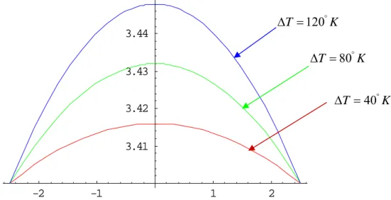
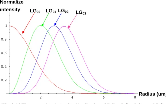
(39) n(r ) = n0 + ∆n −. ∆n 2 ×r R2. (2.61). We calculate the relation of equation 2.61 and show in figure 2.11.. ∆T = 120° K 3.44. ∆T = 80° K 3.43. ∆T = 40° K. 3.42 3.41. -2. -1. 1. 2. Fig. 2.11 The variations of refractive index versus different temperature.. The fundamental mode width is obtained in the form of equation 2.62 [14] where w is the radius of the fundamental mode spot 2w = (. 4 Rλ )1/ 2 π × 2(n0 + ∆n) × ∆n. (2.62). Using equation 2.23 and 2.62 can describe the variation of fundamental mode spot size with increased shown as figure 2.12. We can find that mode spot size is strong affected by the variation of temperature. When ∆T is small there is a rapid drop. It illustrates that only small refractive index change then the laser beam will confined in the core region. The mode spot size will be gradually stable when ∆T more and more large. From equation 2.60 we can describe the near-field mode intensity which is given by * I = ψ mnψ mn. 25. (2.63).
(40) The calculated results of 2-D near-field intensity distribution are shown in figure 2.13 and 1-D intensity profile shown in figure 2.14. From these calculations we can find that fundamental mode intensity distributes in the center of optical aperture and the high order modes intensities distribute in the outer region. 2w( µ m) 20. 15. 10. R = 7.5µ m. R = 5µ m R = 2.5µ m. 5. 20. 40. 60. 80. 100. 120. ∆T (° K ). Fig. 2.12 The function of fundamental mode spot diameter versus temperature.. 7.5. 7.5. 5. 5. 2.5. 2.5. 0. 0. -2.5. -2.5. -5. -5. -7.5. -7.5. -7.5. -5. -2.5. 0. 2.5. 5. 7.5. -7.5. (a) LG00. -5. -2.5. 0. 2.5. (b) LG01. 26. 5. 7.5.
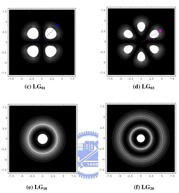
(41) 7.5. 7.5. 5. 5. 2.5. 2.5. 0. 0. -2.5. -2.5. -5. -5. -7.5. -7.5 -7.5. -5. -2.5. 0. 2.5. 5. -7.5. 7.5. -5. -2.5. (c) LG01. 7.5. 5. 5. 2.5. 2.5. 0. 0. -2.5. -2.5. -5. -5. -7.5. -7.5 -5. -2.5. 0. 2.5. 5. 7.5. 5. 7.5. (d) LG03. 7.5. -7.5. 0. 2.5. 5. -7.5. 7.5. (e) LG10. -5. -2.5. 0. 2.5. (f) LG20. Fig. 2.13 Computer calculates the 2-D near-field patterns with fundamental mode spot radius w = 3 um and core region radius R = 5um.. 27.
(42) Normalize intensity. LG00. LG01 LG02. LG03. 1. 0.8. 0.6. 0.4. 0.2. 2. 4. 6. 8. Radius (um). Fig. 2.14 The normalize intensity distribution of LG00, LG01, LG02 and LG03 modes are displayed with 5 um core radius. The calculation modes are individual along its color dash arrows.. 2-3-2. Linearly Polarized Modes in a Dielectric Cylindrical Waveguide. Transverse mode characteristic of VCSEL can also be analyzed by the cylindrical dielectric waveguide theory. It considers a cylindrical waveguide with a homogeneous core refractive index n1 surrounded by an infinite uniform cladding of index n2 shows in figure 2.15.. z. cladding. core. a. n1. n2. ψ r Fig. 2.15 Schematic of a dielectric cylindrical waveguide. 28.
(43) For cylindrical dielectric waveguide with a very small refractive index difference between the core and the cladding (i.e., weakly guiding, n1 ≈ n2 ) is valid for VCSEL [15]. First, we consider the electromagnetic fields U (r , t ) propagate along the longitudinal direction are assumed to have a plane-wave format. U (r , t ) = U (r ) exp( jωt ). (2.64). If we assume a time-harmonic field, the wave equation takes the familiar form ∇ 2U (r ) + n 2 k02U (r ) = 0. (2.65). In cylindrical coordinate, the Maxwell equation can be modified as ∂ 2U (r ) 1 ∂U (r ) 1 ∂ 2U (r ) ∂ 2 (r ) + + 2 + + n 2 k02U (r ) = 0 ∂r 2 ∂z 2 r ∂r r ∂φ 2. (2.66). Due to the translational invariance along the z axis, we can assume that the complex fields propagate along the longitudinal direction is a plane-wave format expressed as. U (r ) = R(r )Φ (φ ) exp(− j β z ). (2.67). where β is the longitudinal propagation coefficient or the z component of the wavevector k. We substitute equation 2.67 into equation 2.66 and use standard separation techniques to find r 2 d 2 R(r ) r dR (r ) 2 2 2 1 d 2 Φ (φ ) 2 + + r ( n k − β ) = − =l 0 R(r ) r 2 R (r ) dr Φ (φ ) dφ 2. (2.68). The term l is called the separation constant or the angular mode number. Thus we can rewrite equation as d 2 Φ (φ ) 2 + l Φ (φ ) = 0 dφ 2. (2.69). d 2 R(r ) 1 dR(r ) l2 2 2 2 ( ) R(r ) = 0 n k + + − β − 0 dr 2 r dr r2. (2.70). Equation 2.70 is Bessel’s differential equation due to its solution is the form of Bessel function. Equation 2.69 has the solution 29.
(44) Φ (φ ) = cos(lφ + α ) or sin(lφ + α ). (2.71). where α is a constant phase shift and assume its value is zero. For step fiber waveguide has a core of radius with higher index ncore a surrounded by a cladding with lower index nclad.. d 2 R(r ) 1 dR(r ) l2 2 2 2 ( ) R(r ) = 0 n k + + − β − core 0 dr 2 r dr r2. 0<r<a. (2.72). d 2 R(r ) 1 dR(r ) l2 2 2 2 ( ) R(r ) = 0 n k + + − β − clad 0 dr 2 r dr r2. r>a. (2.73). The propagation coefficient β must be satisfy k0 ncore > β > k0 nclad , thus equation 2.72 is the Bessel functions of the first kind of order l and equation 2.73 is the Bessel function of the second kind of order l. To simplify the equation above, it is convenient to define 2 2 2 κ 2 = (ncore k02 − β 2 ) × a 2 = (ncore − neff )k02 × a 2. (2.74). 2 2 2 2 γ 2 = ( β 2 − nclad k02 ) × a 2 = (neff − nclad )k02 × a 2. κ max = κ 2 + γ 2 = k0 a n12 − n22 =. 2π. λ0. (2.75). a n12 − n22. (2.76). 2 γ = κ max −κ 2. (2.77). Substituting equation 2.74 and 2.75 into equation 2.72 and 2.73. d 2 R(r ) 1 dR(r ) κ 2 l 2 + + ( 2 − 2 ) R(r ) = 0 dr 2 r dr a r. 0<r<a. d 2 R(r ) 1 dR(r ) γ 2 l 2 + − ( 2 + 2 ) R(r ) = 0 dr 2 r dr a r. r>a. (2.78) (2.79). The solution of equation 2.80 and 2.81 are the family of Bessel functions. R (r ) = AJ l (. κr. R (r ) = CK l (. a. γr a. ). 0<r<a. (2.80). ). r>a. (2.81). To derive the characteristic equation, we apply the boundary conditions. At the core- cladding boundary (r = a) require that the field should be continuous and apply. 30.
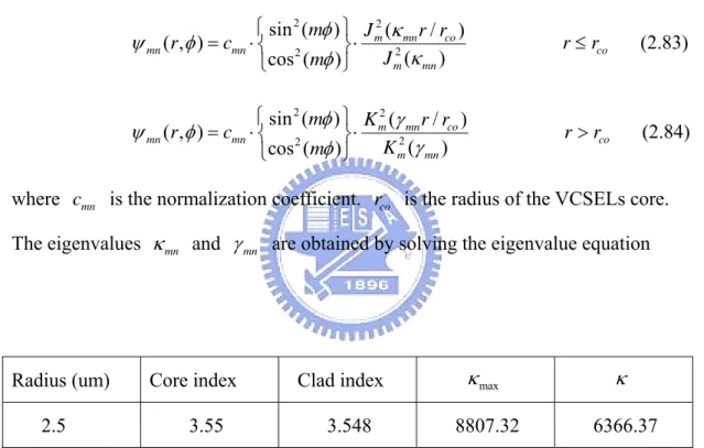
(45) the weakly guided approximation. To satisfy theses two conditions, the characteristic equation is obtained. κ. J j −1 (κ ) J j (κ ). +γ. K j −1 (γ ) K j (γ ). =0. (2.82). where J (κ ) and K (γ ) are Bessel function and Hanker function which has the relations J − j (κ ) = (−1) J j (κ ) and K − j (γ ) = K j (γ ) . The intensity distribution function ψ mn (r , φ ) is given by ⎧ sin 2 (mφ ) ⎫ J m2 (κ mn r / rco ) ⎬⋅ 2 J m2 (κ mn ) φ cos ( m ) ⎩ ⎭. r ≤ rco. (2.83). ⎧ sin 2 (mφ ) ⎫ K m2 (γ mn r / rco ) ⎬⋅ 2 K m2 (γ mn ) ⎩cos (mφ ) ⎭. r > rco. (2.84). ψ mn (r , φ ) = cmn ⋅ ⎨. ψ mn (r , φ ) = cmn ⋅ ⎨. where cmn is the normalization coefficient. rco is the radius of the VCSELs core. The eigenvalues κ mn and γ mn are obtained by solving the eigenvalue equation. Radius (um) 2.5. Core index 3.55. Clad index 3.548. κ max. κ. 8807.32. 6366.37. Table 2.2 The parameters of LP mode calculation.. 31.
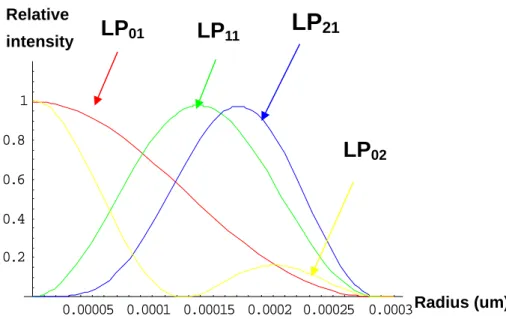
(46) Relative intensity. LP01. LP11. LP21. 1 0.8. LP02. 0.6 0.4 0.2 0.00005 0.0001 0.00015 0.0002 0.00025 0.0003 Radius (um). Fig. 2.17 The intensity distribution of LP01, LP11, LP21, and LP02 modes are displayed the core radius is 2.5 um.. 32.
(47) Chapter3 Single fundamental mode VCSEL from surface modified DBR reflectance. Form chapter 1 we have known that the advantages of single mode VCSELs .Many techniques for single mode VCSELs have been developed. Previous attempts in increasing single mode output power include external reflectors and other optical elements, for example, microlensed structure, multi-oxide layer structure, long monolithic cavity structure, antiguiding structure, graded-index lens structure, surface relief structure and impurity-induced disordering DBR structure [16]. In this section, we will discuss surface relief structure and zinc diffusion induced heterojunction of DBR disorder.. 3-1. VCSEL with shallow etched surface relief structure. Surface relief is an effort to control the transverse modes behavior of VCSEL. It was designed to suppress the higher order transverse modes. By etching a shallow circular ring in the output power window of the top DBR we can modify the reflectance. When we remove material from the top DBR the reflectivity is altered. By choosing the etched depth and relief diameter carefully, we can tailor the cavity properties in such a way to selectively discriminate against unwanted modes. A circular shape is chosen for the relief because that this will match the circularly symmetric profile of the cylindrical cavity mode [17]. In order to successfully optimize the single fundamental mode output,. 33.
(48) information about the overlap between the relief geometry, mode profiles, and the gain distribution is needed. In section 2-3 we have simulated the transverse mode relative intensity distribution with the radius direction. In order to the fundamental mode retain most of its intensity within the low optical loss region we often design the relief radius to be equal to the 1/ e of relative strength of fundamental mode [18]. In section 2-2 we also have discussed the theory of DBR reflectance thus we can use the characteristic of destroy interference to reduce the local DBR reflectance and increase the local optical loss. Fig 3.1 (a) is the reflectance variation with the increasing etching depth and Fig 3.1 (b) is the function of threshold gain versus the etched depth. We can obtain the first minimal reflectance and maximal threshold gain is at the etched depth around 86 nm from the top DBR surface.. 1.005. 1. 0.995. Reflectivity. 0.99. 0.985. 0.98. 0.975. 0.97. 0.965. 0.96. 0. 0.1. 0.2. 0.3. 0.4. 0.5. Etching depth (um). (a). 34. 0.6. 0.7. 0.8.
(49) 0.08. 0.07. Threshold gain (1/um). 0.06. 0.05. 0.04. 0.03. 0.02. 0.01. 0. 0. 0.1. 0.2. 0.3. 0.4. 0.5. 0.6. 0.7. 0.8. Etching depth (um). (b) Fig. 3.1 (a) The reflectivity as a function of the etched depths in the top DBR. (b) The calculated threshold gain as a function of the etched depth in the top DBR.. 3-2. Surface Zinc diffusion to suppress high-order Transverse modes. Zinc enhance AlxGa1-xAs/GaAs interdiffusion has been reported, such as impurity diffusion for edge-emitting lasers fabricated by impurity-induced disordering, bonding by atomic rearrangement, to join dissimilar semiconductors, zinc diffusion for low-resistance mirrors and, regroun over etched pillar vertical cavity lasers. These applications of zinc diffusion can result in high-performance optoelectronic devices.. 35.
(50) 3-2-1. Temperature induces AlxGa1-xAs/GaAs inter-diffusion. High temperature induces the concentration of aluminum and gallium of AlxGa1-xAs/GaAs hetero-junction or super-lattice redistribute thus the interface of AlxGa1-xAs/GaAs to be disordered has been reported [19]. Such phenomenon is called inter-diffusion. During a high-temperature process the aluminum and gallium get enough kinetic energy and left their original site away. In 1980, Chang and Koma pointed out the AlAs/GaAs inter-diffusion coefficient is in the range of 10-17 ~ 10-18 cm2 s-1 at 800 ℃ and 10-14 ~ 10-15 cm2 s-1 at 1100 ℃. To model the inter diffusion of Al and Ga in a DBR, P. D Floyd and J. L. Merz solved Fick’s equation with a constant inter-diffusion coefficient DAl-Ga expressed as ∂X Al ∂ 2 X Al = D Al −Ga ∂t ∂z 2. (3.1). According to our DBR structure, we set the initial condition of a square well Al mole fraction profile XAl(z,0) shown as figure 3.2 (a) where L z and LB are the thicknesses of Al0.12Ga0.88 As and AlAs . The final condition which can be defined as X Al ( z , ∞) =. L B X B + LZ X Z L B + LZ. (3.2). which shown in figure 3.2 (b). The boundary condition can be given by. X Al ( z, t ) = X Al ( z + T , t ). (3.3). The general solution for the Al profile in the mirror is given by. X Al ( z, t ) = X Al ( z , ∞) +. n nπLZ 1 2πnz ( X Z − X B )∑ cos(nπ ) × sin( ) cos( ) π T T 1 n. 2. 2π × exp[−( ) 2 nL2D ] T. (3.4). where LD = D Al −Ga t is the diffusion length [20]. Figure 3.3 are the calculation of temperature induced Al-Ga inter-diffusion.. 36.
(51) AlAs XAl mole fraction. LB = 69.2 nm. 1. 0.8. 0.6. 0.4. 0.2. LZ = 61.2 nm 100. 200. 300. 400. 500. 600. 700. depth (nm). Al0.12Ga0.88 As. Fig. 3.2 (a) The initial condition of XAl (z,0) mole fraction.. XAl mole fraction 1.2. 1. 0.8. 0.6. 0.4. depth (nm) 0.2. 100. 200. 300. 400. 500. 600. 700. Fig. 3.2 (b) The final condition of XAl (z,∞) mole fraction. We use the relation and table 3.1 to describe the refractive index as a function of 37.
(52) the depths shown in figure 3.6 (c).. n2 = A +. B − Dλ02 λ −C. [21]. 2 0. GaAs. (3.9). AlxGa1-xAs. A. 10.9060. 10.9060-2.92x. B. 0.97501. 0.97501. C. 0.27969. (0.52868-0.735x)2 for x < 0.36 (0.30386-0.105x)2. 0.002467. D. for x > 0.36. 0.002467 (1.41x+1). Table. 3.1 Sellmeier coefficients for refractive index calculation in AlxGa1-xAs.. 24 hr. 24 hr. 96 hr. 96 hr. 192 hr. 192 hr 1. Al mole fraciton. 0.8. 0.6. 0.4. 0.2. 0 0. 100. 200. 300. 400. 500. 600. diffusion length (nm). Fig 3.3 (a) The variation of Al mole fraction with different diffusion time.. 38. 700.
(53) 3.6 24 hr 96 hr. 24 hr. 96 hr. 192 hr. 192 hr. 3.5. refractive index. 3.4. 3.3. 3.2. 3.1. 3 0. 100. 200. 300. 400. 500. 600. 700. depth (nm). Fig. 3.3 (b)The variation of refractive index with different diffusion time.. 1 24 hr. 24 hr 96 hr 192 hr. 96 hr. 0.9. 192 hr 0.8. 0.7. Reflecance. 0.6. 0.5. 0.4. 0.3. 0.2. 0.1. 0 750. 800. 850. 900. 950. 1000. wavelength (nm). Fig 3.3 (c)Calculation of reflectivity spectra with different diffused time. 39.
(54) 3-2-2. Diffusion Zn enhance AlxGa1-xAs/GaAs inter-diffusion. From last section, we obtain the inter-diffusion coefficient which only caused by temperature is quite small. Thus we diffuse impurity zinc to enhance the rate of AlxGa1-xAs/GaAs inter-diffusion [22]. There are several models to describe the impurity induced disordering. All are based on the fact that Zn diffuses via the interstitial-substitutional mechanism in AlxGa1-xAs semiconductors [23]. Zn moves as interstitial donors (Zni+) and after incorporation on to the on to the group 3 sublattice forms substitutional acceptors (Zns-). Two different mechanisms have been proposed for the incorporation of interstitial Zn into the substitutional site. The first is the “dissociative” mechanism Zni+ + V3( Al ,Ga ) ⇔ Zn3− + 2h +. (3.5). where V3(Al,Ga) and Zn3− represent a vacancy and a zinc atom on a group 3 site ( i.e. either an aluminium or a gallium site ) and h is a hole. This mechanism involves group 3 vacancies. The second is the “kick-out” mechanism Zni+ ⇔ Zns− + I 3( Al ,Ga ) + 2h +. (3.6). which involves group 3 interstitials I 3( Al ,Ga ) . From equation 3.6 the group 3 interstitial is created directly by an interstitial Zn moving into a group 3 lattice site through the kick-out mechanism. Since the substitutional Zn3− concentration due to Zn diffusion in AlxGa1-xAs is typically ≅ 5 × 1019 cm-3 thus the Zn-diffused regions will contain a high concentration of group 3 intersitital defects [24]. These two mechanisms of zinc diffusion are shown in figure 3.5 (a), (b), and (c). The dissociative mechanism also exist group 3 atoms inter-diffusion. For Al-Ga inter-diffusion we have 40.
(55) Gav ‹ Gav + ( Ali + Gav ) ‹ ( Gav+ Ali) + Alv‹ Alv. (3.7). and an Al atom has moved. Gai ‹ Gai + (Alv + Ali) ‹ ( Gai + Alv) + Ali ‹ Ali. (3.8). and an interstitial Ga atom has exchanged with a subsitutional Al atom, promoting an Ali [25]. The inter-diffusion is shown in figure 3.5 (d), (e), and (f). It was suggested that the vacancy part of the complex could take part the self-diffusion process i.e. that the presence of the zinc could effectively increase the concentration of group 3 vacancies and hence aid inter-diffusion. Ga. Al. V3(Al,Ga). Zns-. Zni+. Al0.12Ga0.88As Kick-out. AlAs. (a). (b). Gai. Ali. (c). (d). 41. dissociative.
(56) Alv. Gav. (e). (f). Fig. 3.4 The kick-out, interstitial, and substitutional mechanism of zinc diffusion.. We use selective Zn diffusion through top DBR then impurity will induce the disordering of the aluminum mole fraction. In optical characteristic this impurity induced disorder will cause the decrease of the reflectivity. Owing to increased interstitial defects AlxGa1-xAs/AlAs heterojunction disorder is localized to the Zn diffusion regions [26]. We consider each site has different zinc enhance inter-diffusion time and assume the effective zinc diffusion coefficient DZn = 500 nm2/s in AlxGa1-xAs [27]. All of the calculated parameters are shows in table 2.1.. Diffusion time (min). 8 min. 16 min. 32 min. 60 min. Diffusion length (nm). 490 nm. 693 nm. 980 nm. 1342 nm. Zinc enhance time t (z). 8 × 60 −. z2 500. 16 × 60 −. z2 500. 32 × 60 −. z2 500. 60 × 60 −. z2 500. Table. 3.2 The parameters of Zn enhance inter-diffusion.. Figure 3.5(a) shows the Zn diffusion depth versus Zn enhance inter-diffusion 42.
(57) time. Combining this relation with equation 3.4 and assuming the effect inter-diffusion coefficient DAl-Ga = 0.4 nm2/s with 600℃ we can calculate the variation of Al mole fraction with zinc enhance inter-diffusion. Figure 3.5(b) is the profile of Al mole fraction with the zinc diffusion. The longitudinal axial is aluminum concentration and transverse axial is the depth of DBR. We observe that the variation of aluminum mole fraction is more violent near the surface and is gentle in the deeper location of the DBR with diffusion time. The refractive index and the reflectance of top BDR will be changed in the same time. Then we use the transmit matrix which has discussed in chapter 2 to calculate the reflectance spectral of top DBR with different diffused time. Figure 3.5 (d) is the calculated reflectivity spectra for a 20.5 period Al0.12Ga0.88As/AlAs DBR for several. 4000. 3500. 60 min Zn enhance time (sec). 3000. 2500. 32 min 2000. 1500. 16 min 1000. 8 min 500. 0. 0. 200. 400. 600. 800. diffusion length (nm). (a). 43. 1000. 1200. 1400.
(58) 8 min. 16 min. 32 min. 60 min. 1. 0.9. 0.8. Al mole fraciton. 0.7. 0.6. 0.5. 0.4. 0.3. 0.2. 0.1. 0. 200. 400. 600. 800. 1000. 1200. 1400. 1600. 1800. 2000. diffusion length (nm). (b). 3.55. 8 min. 16 min. 32 min. 60 min. 3.5. 3.45. refractive index. 3.4. 3.35. 3.3. 3.25. 3.2. 3.15. 3.1. 3.05. 0. 200. 400. 600. 800. 1000. depth (nm). (c). 44. 1200. 1400. 1600. 1800. 2000.
(59) 8 min 16 min 32 min 60 min. 1. 0.9. 0.8. Reflecance. 0.7. 0.6. 0.5. 0.4. 0.3. 0.2. 0.1. 0 750. 800. 850. 900. 950. 1000. wavelength (nm). (d) Fig. 3.5 The calculation of Zinc enhaces 20.5 Al0.12Ga0.88As/AlAs DBR(a) calculation of the Zn enhance inter-diffusion time with different site, (b) Al mole fraction as a function of diffusion length and different diffusion time, (b) refractive index as a function of diffusion length and different diffusion time, and (d) calculation of reflectivity spectra with different diffusion time.. 45.
(60) Chapter4 Experiment. 4-1. The experiment of zinc diffusion and shallow surface etching Before the fabrication of VCSEL devices, we do several experiments to compare. the reflectance of zinc diffusion and shallow surface etching. Thus we can choose the best condition to fabricate VCSEL devices.. 4-1-1 The experiment of zinc diffusion We use the most common way to control the atmosphere where a diffusion experiment is carried out is using the so-called closed ampoule. A schematic of a closed ampoule is shown below. A plug is formed in a similar fashion using tubing with a slightly smaller outer diameter than the inner diameter of the shell. Desired diffusion source (zinc and arsenic) and text wafer are placed in the ampoule shell at the sealed end. The plug is then inserted and using vacuum pump to carry out the atmosphere which maintains at 4 × 10 −6 torr .Then a seal is made between the plug and shell using a hydrogen-oxygen torch.. Fig 4.1. Schematic of sealed ampoule with gray semiconductor diffusion sample sealed in small volume.. Figure 4.2 and 4.3 are the SEM profile of 8 min and 16 min zinc enhance interdiffusion. We can find that the heterojunction of DBR is more disordered near the wafer surface and the degree of disorder is diffused 16 min larger than 8 min.. 46.
(61) (a). (b) Fig. 4.2 SEM observations of the VCSEL sample, (a) after Zn diffusion 8 min (b) after Zn diffusion 16 min at 600 ℃. 47.
(62) We also measure the reflectance spectral of 8 min, 16 min and non diffused wafer shown as figure. From the reflectance spectral we find that the longer diffused time has lower reflectance. From figure 3.6 (d) we find that the longer diffused time has the lower reflectance and smaller stop band. From figure 4.2 (c) we observed that there is an amorphous film adhere to the surface of wafer. Figure 4.3 is the zinc diffusion of top DBR with 8 and 16 min diffusion time in the quartz ampoule along with the elemental arsenic for overpressure and zinc powder. We can obtain the reflectivity and stopband width is decreased with diffusion time is increased.. Nondiffusion 8 min 16 min. 1.0. Reflectance. 0.8. 0.6. 0.4. 0.2. 0.0. 740. 760. 780. 800. 820. 840. 860. 880. 900. 920. Wavelength (nm). Fig. 4.3 The reflectance spectral of 8 min, 16 min, and zero diffused time.. 48.
(63) 4-1-2 The experiment of shallow surface etching. The first layer of our VCSEL wafer is GaAs capping layer ( ≈ 110nm ). We use ICP ( Inductively coupled plasma ) to etch the top DBR surface. From the calculation of figure 3.1 (a) we can find that the first local minima reflectance is about at the depth of 85 nm. The recipe of ICP is that 5 min can etch 1500 A GaAs film. From the recipe we can forecast that it needs about 130 sec to arrive the designed depth 85 nm. Figure 4.4 is the reflectance spectral with different etched time. We find that it is the local lowest reflectance with 130 sec etched time. At 120 sec and 140 sec etched times we find that the reflectance is clearly increased. This phenomenon matches with our calculation of figure 3.1.. 140 and 120sec. 130 sec 120 sec 120 sec 120 sec 130 sec 130 sec 130 sec 140 sec 140 sec 140 sec. 1.0. Reflectance. 0.8. 0.6. 0.4. 0.2. 0.0. 740. 760. 780. 800. 820. 840. 860. 880. 900. 920. Wavelength (nm). Fig. 4.4 The reflectance spectral of 120 sec, 130 sec, and 140 sec etched time.. 49.
(64) 4-2 Specific Process step of fabrication of VCSEL devices 1. Wafer Clean. :. ACE(Acetone) 5’, IPA(Isopropyalcohol) 2’, B.O.E 5’. SiO2 Deposition. :. PECVD 2800 A. Lithography. :. Baking 100 ℃ 5’ Photoresist 500 rpm 5”, 2000 rpm 25” Exposure 10” Develop 1’30” FHD5 Baking 120 ℃ 10’. SiO2 Etching. :. ICP. Remove PR. :. ACE 10’, IPA 2’. 2. Si3N4 Deposition. :. PECVD 1000A. Lithography. :. Baking 120 ℃ Photoresist 500 rpm 5”, 2000 rpm 25” Exposure 4” Develop 1’30” FHD5 Baking 120 ℃ 10’. SiNX Etching. :. ICP. Remove PR. :. ACE 10’, IPA 2’. 3’40”. 3. (1) Zinc Diffusion Clean quartz Stuff. :. HF. 10’. :. Baking 120’ Zn / As , wafer. 50.
(65) (2) Surface relief Surface etching. :. ICP 2’ 10”. Clean. :. ACE 5’, IPA 2’. 4. Lithography. :. Baking 120 ℃ 5’ Photoresist 500 rpm 5” , 3500 rpm 25” Baking 100 ℃ 1’ Exposure 4" Baking 120 ℃ 2’ Exposure 35” Develop 40” Baking 120℃. Clean. :. CH3COOH / NH4F / H2O 1’. Evaporation. :. Ti / Pt / Au ~3800A. Lift off. :. ACE. Evaporation. :. Ti / Pt / Au ~3800A. Annealing. :. 420 ℃. 5’. :. Baking. 120 ℃ 5’. ( p–contact ). 5’ , IPA 2’ ( n–contact ). 5. Lithography. Photoresist 1000 rpm 3” , 4000rpm 35” Baking 120 ℃ 5’. Implantation Remove PR. : :. Exposure 17” Develop 3’ 30” Baking 120 ℃ 10’ H+ 1015 cm-2 230 and 300 keV ACE 5’, IPA 2’, H2SO4 3’ (heating 40℃). 51.
(66) (a). (b1). (b2). (c1). (c2). (d1). (d2). (e1). (e2). Fig. 4.5 The process procedures of the device with the (a) oxide deposition, (b1)(b2) shallow etch and zinc diffusion, (c1)(c2) metal evaporation, (d1)(d2) ion implantation, and (e1)(e2) the complete VCSELs. 52.
(67) (a). (b) Fig. 4.6 The top view images of the devices (a) the surface relief structure and (b) the Zn diffusion structure.. 53.
(68) 4-3 Failure analysis of 850 nm VCSEL. The VCSEL device series resistance is mainly determined by the p-ohmic contact and p-DBRs, the detradation of I-V characteristics ought to come from the degradation of these two parts. We measure the I-V curve before ion-implant shown in figure 4.6 . This diagram tells us that the series resistance are about 16.9 and 34 Ω of surface relief and zinc diffusion structures. The resistance of zinc diffusion VCSEL is larger than surface relief structure. The most likely explanation is that the diffusion VCSEL is grown an amorphous film when we use a hydrogen-oxygen torch. Thus the series resistance is increase.. Zinc diffusion Surface relief. RS = 34 W. 5. Voltage (V). 4. 3. RS = 16.9 W. 2. 1. 0 0. 10. 20. 30. 40. 50. 60. 70. 80. Current (mA). Fig. 4.7 Measurements of VCSELs I-V curve with the surface relief structure and the zinc diffusion structure.. 54. 90.
(69) After ion-implanted and 10 min annealing we find that the I-V characteristic of VCSEL devices are almost open circuit. This indicates that the series resistance of device is much larger than non ion-implant. The electrical degradation is believed to be the damage of p-ohmic contact and p-DBRs. Because excessive vacancies are produced by proton bombardment at the region of metal-semiconductor interface and the vacancies distribution also has a long tail covering the most of p-DBRs. These vacancies will affect the electro-migration processes and cause the long term degradation of ohmic contact then give rise to the gradual increase in device series resistance. We found that there are still devices with smaller series resistance such I-V curve shows in figure 4.8. These devices are with ion-implanted aperture 25 um and contact aperture 18um. Our inference is that owing to the larger undamaged metal-semiconductor interface.. RS = 130 Ω. 2.0. Voltage (V). 1.5. 1.0. 0.5. 0.0. -0.5 0.000. 0.002. 0.004. 0.006. 0.008. 0.010. Current (A). Fig. 4.8 Measurement of VCSELs I-V curve of surface relief structure with ion-implanted aperture 25 um, contact aperture 18 um and surface relief diameter 9um. 55.
(70) We also measure the L-I curve shows in figure 4.8. We find that the output power is the characteristic of light emitting diode. The phenomenon is due to the large optical loss caused by top DBR shallow etched. 0.05. Output power (mW). 0.04. 0.03. 0.02. 0.01. 0.00. 0.000. 0.005. 0.010. 0.015. 0.020. 0.025. 0.030. Current (A). Fig. 4.9 The L-I curve of surface relief structure with ion-implanted aperture 25 um, contact aperture 18 um and surface relief diameter 9um.. 56.
(71) Chapter5 Conclusion We fabricated 850 nm ion-implanted VCSELs with surface relief and zinc diffusion adjustment. The DBR threshold gain, DBR reflectance, and near field patterns were calculated. Optical characteristics of structures with shallow etched surface and zinc diffusion onto DBR were simulated. We have calculated the threshold gain and found that the reflectance of top DBR decrease from 0.9985 to 0.98 then threshold gain will rapidly increase from 825 cm-1 to 4853 cm-1. We derived Laguerre-Gaussian mode and linear polarization mode to calculate the distribution of mode intensity. The relation of mode spot size versus temperature was also concerned. We find the temperature will cause refractive index gradually reduce from the center to edge of the core. The mode size will gradually be a constant. We used shallow surface etched and zinc diffused to reduce the reflectance of DBR. In the shallow surface etched structure, we find that the reflectance is not gradually decrease with the etched depth. The first local minimum reflectance is at 86 nm. We used ICP to shallow tech the DBR only 120, 130, and 140 seconds then observed the reflectance decreased and etched 130 seconds the reflectance has local minimum. In Zn diffusion structure, diffuse zinc to enhance the inter-diffusion and increase AlxGa1-xAs/AlAs disorder rate. In 600 ℃ quartz ampoule, we diffused 8 min and 16 min, then we find the reflectance decrease to 0.8 and 0.6. Because an amorphous films are on the DBR the reflectance is lower than that we calculated. We used the two methods to fabricate single mode VCSELs. We have measured 15W and 34W series resistance before ion-implanted process. Because of the large series 57.
(72) resistance of VCSELs after the ion-implanted process, almost devices can’t work. We measured the other devices and found that the characteristics of output power are LEDs. The maximum output power is 0.04 mW. It may be caused by the decrease of reflectance and increase the threshold gain. Thus these devices are not easy to work.. 58.
數據

+7
相關文件
Reading Task 6: Genre Structure and Language Features. • Now let’s look at how language features (e.g. sentence patterns) are connected to the structure
利用 determinant 我 們可以判斷一個 square matrix 是否為 invertible, 也可幫助我們找到一個 invertible matrix 的 inverse, 甚至將聯立方成組的解寫下.
Then, we tested the influence of θ for the rate of convergence of Algorithm 4.1, by using this algorithm with α = 15 and four different θ to solve a test ex- ample generated as
Numerical results are reported for some convex second-order cone programs (SOCPs) by solving the unconstrained minimization reformulation of the KKT optimality conditions,
Particularly, combining the numerical results of the two papers, we may obtain such a conclusion that the merit function method based on ϕ p has a better a global convergence and
Then, it is easy to see that there are 9 problems for which the iterative numbers of the algorithm using ψ α,θ,p in the case of θ = 1 and p = 3 are less than the one of the
By exploiting the Cartesian P -properties for a nonlinear transformation, we show that the class of regularized merit functions provides a global error bound for the solution of
When ready to eat a bite of your bread, place the spoon on the When ready to eat a bite of your bread, place the spoon on the under plate, then use the same hand to take the
