Manuscript received January 15, 2007 0098 3063/07/$20.00 © 2007 IEEE
Design of Memory Sub-System with Constant-Rate Bumping
Process for H.264/AVC Decoder
Chih-Hung Li, Wen-Hsiao Peng, and Tihao Chiang
Abstract — In this paper, we propose an efficient memory
sub-system and a constant-rate bumping process for a H.264/AVC decoder conforming to High profile@ Level 4. To efficiently utilize the throughput of external DRAM, a synchronization buffer is employed as a bridge for reformatting the read/write data exchanged between the on-chip hardware and the off-on-chip DRAM. In addition, we optimize the issues of read/write commands and adaptively enable the auto-precharge function by monitoring the motion information of a submacroblock. Furthermore, a regulation buffer with size comparable to the decoded picture buffer is created to ensure a constant output rate of decoded pictures for any conformed prediction structures. Along with other modules, the proposed scheme is verified at system level using transaction level modeling (TLM) technique. Statistical results show that synchronization buffer of larger block size provides higher memory efficiency, less access cycles and power dissipation. However, the granularity of 8x8 block size provides better trade-off among cost, efficiency, power, and real-time requirement.1
Index Terms — H.264/AVC, DRAM controller, Bumping process, Transaction level modeling.
I. INTRODUCTION
The H.264/AVC decoder [1], which incorporates advanced inter predictions, demands higher bandwidth for external memory due to intensive data transfer and less efficient DRAM access. The intensive data transfer is introduced by more accurate sub-pel interpolation, motion compensation of smaller block size, as well as motion field inference of temporal direct modes in B slices. On the other hand, the less efficient DRAM access is caused by motion compensation of variable block size and adaptive temporal prediction with multiple reference frames. As compared with MPEG-1/-2/-4, the frequency of DRAM access is increased by 2x to 16x. Moreover, the ratio of row-miss in the external DRAM is increased considerably.
With intensive and irregular DRAM access, the memory sub-system that acts as a bridge for exchanging data between the on-chip hardware and the off-chip DRAM becomes the 1 Chih-Hung Li is with the Institute of Electronics, National Chiao-Tung
University, 1001 Ta Hsueh Road, Hsinchu, Taiwan 300, ROC (e-mail: [email protected]).
Wen-Hsiao Peng is with the Department of Computer Science, National Chiao-Tung University, 1001 Ta Hsueh Road, Hsinchu, Taiwan 300, ROC (e-mail: [email protected]).
Tihao Chiang is with the Department of Electronics Engineering, National Chiao-Tung University, 1001 Ta Hsueh Road, Hsinchu, Taiwan 300, ROC (e-mail: [email protected]).
performance bottleneck in the real-time applications. Several literatures are dedicated to improve the efficiency of DRAM access. In [2][3], the probability of page miss is minimized by storing reference frames in the DRAM with checkerboard pattern; that is, the adjacent groups of pixels are stored in different banks with interleaved order. Furthermore, in [4] the luminance and chrominance components are stored in two separate DRAMs so as to gain sufficient bandwidth. However, the auto precharge function is enabled after each DRAM access; consequentially, 2~4 DRAM must be used to match the bandwidth of the on-chip modules.To effectively schedule the DRAM commands, in [5] a history-based prediction scheme is used to enable auto precharge function according to the run-time behavior of the memory access. However, the prediction accuracy is reduced significantly by the irregular data access of H.264/AVC.
In addition, the irregular and variable-rate bumping process of H.264/AVC decoder further increases the complexity of memory management. Different from prior video coding standards in which the decoder can output pictures according to the timestamps in the picture or slice header, the network abstraction layers (NAL) in H.264/AVC contain no timing information. Thus, the bumping process manages the output of the decoded pictures such that the output order conformance is guaranteed. Currently, the bumping process of decoded pictures is invoked when a decoded picture is to be stored in the decoded picture buffer (DPB) while there is no empty space. Multiple decoded pictures could be output simultaneously while for some time instances none of the pictures are output. The variable output rate causes extremely varying bandwidth for DRAM access.
In this paper, we propose an efficient memory sub-system and a constant-rate bumping process for a H.264/AVC decoder conforming to High profile and Level 4. To increase the on-chip bus utilization while maximizing the effective throughput of DRAM access, a synchronization buffer is employed for re-formatting the read/write data exchanged between the on-chip modules and the off-chip DRAM. The efficiency of DRAM access and the associated power dissipation as well as the hardware cost are analyzed when the synchronization buffer is designed at different levels of granularity, including 4x4, 8x8, 16x16 (1 macroblock), and 32x16 (2 macroblocks). In addition, we optimize the issues of DRAM commands and adaptively enable the auto-precharge function by monitoring the motion information of a submacroblock. Further, for lower probability of row miss, the reference frames are partitioned into multiple blocks of size 32x32 and stored in the DRAM with checkerboard pattern. On
the other hand, to ensure a constant output rate of decoded pictures, we create a regulation buffer with size being equal to that of the DPB. Along with other modules, the proposed scheme is verified at system level using transaction level modeling (TLM) technique.
The contributions of this paper include (1) a platform-based architecture of H.264/AVC decoder, (2) an efficient design of memory sub-system for High profile at Level 4, (3) a constant-rate bumping process for any conformed prediction structures, (4) an external memory controller for increasing the effective bandwidth of the off-chip DRAM. The rest of this paper is organized as follows: After providing the overall architecture of the proposed H.264/AVC decoder in Section II, Section III presents the details of the memory sub-system. Then, Section IV proposes a constant-rate bumping process. After that, Section V addresses the implementation issues. Finally, Section VI and Section VII give the simulation results and some concluding remarks.
II. SYSTEM ARCHITECTURE OF H.264/AVCDECODER
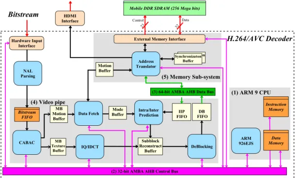
Fig. 1 shows the proposed system architecture, which can mainly be divided into 5 different parts including (1) the ARM 9 CPU, (2) the 32-bit AHB control bus, (3) the 64-bit AHB data bus, (4) the video pipe, and (5) the memory sub-system. Among the 5 different parts, the ARM 9 CPU acts as the data flow controller, which programs and monitors the status of the video pipe through the 32-bit control bus. On the other hand, the video pipe performs the decoding of NAL units according to the configuration setup by the CPU. Each decoded picture is further stored in the external DRAM and then removed from the DRAM according to our constant-rate bumping process. In addition, the reference pictures and the
reconstructed pixels in the adjacent blocks for inter/intra prediction and de-blocking filtering are also stored in the external DRAM. Thus, the external memory not only acts as DPB, but also plays the role of the output regulation buffer. For the intensive data transfer between the video pipe and the external DRAM, a 64-bit data bus is employed. Particularly, to increase the on-chip bus utilization while maximizing the effective throughput of DRAM access, the memory sub-system uses a synchronization buffer to reformat the read/write data before performing DRAM access through the external memory interface. The following details the operations in the video pipe and the memory sub-system.
A. Operations of Video Pipe
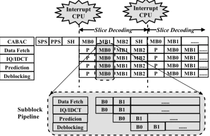
As shown in Fig. 1, the video pipe mainly consists of 5 different modules CABAC, IQ/IDCT, Data Fetch, Intra/Inter Prediction, and De-Blocking Filter, where all the modules are connected with backdoor-to-backdoor channels and the data exchange between the modules are done block-by-block. The scheduling of video pipe is illustrated in Fig. 2. Specifically, we adopt a hybrid pipeline design where the CABAC operates at the macroblock level while the other modules in the video pipe communicate at the 8x8 block level, including one 8x8 luminance block and two 4x4 chrominance blocks.
In detail, the operations of the video pipe begin with the decoding of the control information such as the sequence parameter set, the picture parameter set, and the slice header. The control signals are then acquired by the ARM 9 CPU for programming each module in the video pipe.According to the instructions, the CABAC performs the decoding of motion information and transform coefficients for each macroblock. After that, the Data Fetch module infers the motion vector for (2) 32-bit AMBA AHB Control Bus
External Memory Interface Mobile DDR SDRAM (256 Mega bits)
CABAC
(3) 64-bit AMBA AHB Data Bus
Bitstream FIFO ARM 926EJS Instruction Memory IQ/IDCT MB Texture Buffer MB Motion Buffer
Data Fetch Intra/InterPrediction
Subblock Reconstruct Buffer DeBlocking IIP FIFO DB FIFO Address Translator Hardware Input Interface (4) Video pipe HDMI Interface Synchronizaton Buffer (5) Memory Sub-system Data Memory H.264/AVC Decoder Bitstream Synchronizaton Buffer NAL Parsing 23 32 Data Control Mode Buffer Motion Buffer (1) ARM 9 CPU
each subblock and inputs the data to the address translator for generating the physical DRAM address. While the memory sub-system fetches the data for the next pipeline, the IQ/IDCT module performs inverse quantization and transformation to obtain the residue data. In addition, the Intra/Inter Prediction module generates the predictor by performing directional prediction or sub-pel interpolation using the reference pixels pre-fetched in the synchronization buffer of the memory sub-system. Lastly, the De-Blocking Filter module reconstructs the subblock by adding the residue data to the predictor and then performs the de-blocking filtering according to the boundary strength. For the reordering of decoded pictures, the reconstructed subblock is sequentially written back to the external DRAM through the memory sub-system.
B. Operations of Memory Sub-System
The memory sub-system consists of an address translator, a memory interface, and a synchronization buffer. The address translator takes the motion vectors from the Data Fetch module and generates the physical DRAM address for the external memory interface, which further issues the DRAM commands and enables the auto-precharge function adaptively. Particularly, for concurrent DRAM access and video decoding, all the read/write data required for the video pipe will be firstly fetched in the synchronization buffer. Such a buffer is also used for reformatting the read/write data exchanged between the video pipe and the off-chip DRAM so as to simultaneously increase the on-chip bus utilization while maximizing the effective throughput of DRAM access. Specifically, for the implementation of the synchronization buffer, two banks of SRAM are used. From the experiments, increasing the size of the synchronization buffer improves the efficiency of DRAM access; however, it also introduces higher cost for the on-chip hardware. To find the best design trade-off, in Section VI, the efficiency of DRAM access and the associated power dissipation as well as the hardware cost are analyzed when the synchronization buffer is designed at different levels of granularity.
III. DESIGN OF MEMORY SUB-SYSTEM
In this section, we present the proposed memory sub-system, including (1) an interleaved data arrangement scheme for improving the efficiency of DRAM access, (2) an external memory interface for the control of mobile DDR SDRAM, (3) a synchronization buffer for data cache, and (4) a constant-rate bumping process for in-order, regular output of decoded pictures.
A. Interleaved Data Arrangement
Data arrangement in the external memory is critical to the effective bandwidth that can be achieved as well as the power consumption incurred for the DRAM access. An inefficient data arrangement increases the probability of row miss, for which the data in the sense amplifier must be firstly precharged before another row is activated causing longer latency for DRAM access and lower effective bandwidth. In addition, the row activation and the precharge operation induce more power consumption than normal read/write access. Equation (1) illustrates the energy consumption during the DRAM access [5], where Nactive, Nprecharge, and N are the rw number of active, precharge, and read/write access respectively. rw rw e prech e prech active active dynamic N E N E N E E = . + arg . arg + . (1)
According to the data sheet in [6], each active or precharge command typically expends 14,000 pJ while each read/write access consumes only 2,000 pJ; that is, the active and precharge commands require 7x more energy consumption than read/write access. As a result, an efficient data arrangement must simultaneously minimize the probability of row miss and reduce the number of read/write access.
In this paper, we propose an interleaved data arrangement based on the checkerboard pattern to minimize the probability of row miss. As shown in Fig. 5, the luminance component of each reference picture is partitioned into multiple blocks of size being 32x32 (i.e., 4 macroblocks) and the spatially adjacent blocks are stored respectively in the 4 different banks of DRAM. When accessing a block for the motion compensation as the example in Fig. 5, at most one row is activated for each bank such that the number of row-miss is minimized. In addition, the row activations for different banks can be overlapped thereby the latency can be reduced. Similarly, the same arrangement is applied to the chrominance components. In particular, because of lower resolution, the Cb and Cr components are mixed together when forming the 32x16 block. Moreover, since the chrominance block is processed right after a luminance block, the interlaced memory mapping allocates the luminance and chrominance pixels and motion data of a 32x32 block into the same row of a bank such that the row activated for the data access of a luminance block remains open during the processing of the following chrominance block. Additional precharge and RAS (Row Address Strobe) latency could be eliminated due to such arrangement. Subblock Pipeline CABAC IQ/IDCT Prediction Deblocking Data Fetch SH MB0 MB1 MB2 SH MB0 MB1 SPS PPS P MB0 MB1 MB2 P MB0 MB1 P MB0 MB1 MB2 P MB0 MB1 P MB0 MB1 MB2 P MB0 MB1 P MB0 MB1 MB2 P MB0 MB1 Slice Decoding IQ/IDCT Predicion Data Fetch B0 B1 ... B0 B1 ... B0 B1 ... Deblocking Interrupt CPU Interrupt CPU Slice Decoding ... ... ... ... ... B0 B1 ...
Fig. 2. The scheduling of the video pipe where SPS denotes the sequence parameter set, PPS denotes the picture parameter set, SH denotes the slide header, and P means that CPU programs the individual module.
To fulfill the requirements, we define a group of 4 spatially adjacent macroblocks as a luminance row block and the pixels in a luminance row block are stored in the same row of a bank. Similarly, the same arrangement is applied for the associated chrominance components. In particular, because of lower resolution, each Cb and Cr block of size 16x16 are mixed together to form a chrominance row block of size 32x16. The samples in a chrominance row block are appended after those in the associated luminance row block. Moreover, the remaining space of a row is allocated for the storage of motion information including motion vectors and reference indexes.
B. External Memory Interface
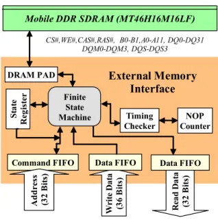
To minimize the extra cycles induced by the row miss and the bank miss, we propose an external memory interface optimized for the control of the mobile DDR SDRAM. As
shown in the functional block diagram of Fig. 3, the physical addresses from the address translator are stored in a specific command FIFO (First-In-First-Out) such that auto precharge function can be used more efficiently.The finite state machine (FSM) combined with the state register, timing checker, and counter generates the corresponding DRAM commands under the considerations of the timing constraints and the power consumption. The read/write data FIFO are included to synchronize the latency of row activation, burst data, and video processing operations.
1) Adaptive Auto Precharge Function
The auto precharge function of DRAM allows the memory controller to perform the read/write commands in a more compact way so that the latency of DRAM access can be reduced. Normally, during the DRAM access, the row being accessed will be remained activated for the subsequent accesses unless a refresh command is received. With the auto precharge function, one can decide whether the row being accessed should be precharged automatically at the end of a read/write burst. Generally, the decision for enabling the auto precharge function is dependent on consecutive commands. For instance, the auto precharge function will be a benefit
CS#,WE#,CAS#,RAS#, B0-B1,A0-A11, DQ0-DQ31 DQM0-DQM3, DQS-DQS3
External Memory
Interface
Wri te Da ta (3 6 B it s) Rea d Da ta (3 2 B it s)Command FIFO Data FIFO Data FIFO
Timing Checker NOP Counter St at e Reg is ter Ad d res s ( 32 B it s) DRAM PAD Finite State Machine Mobile DDR SDRAM (MT46H16M16LF)
Fig. 3. The functional block diagram of the external memory interface.
Hit Bank Row Column
1 2 100 50 1 1 100 80 0 1 91 60 1 2 100 28 0 2 100 60 2 100 60 2 101 60 Command FIFO = = Incomming B R Hit = B' + R Read counter
Fig. 4. The command FIFO for the detection of the row miss.
Current 8x8 Blcok 64 Columns for Motion Data 128 Columns for Chrominance Pixels
Micron Mobile DDR SDRAM (MT46H16M16LF)
16 B3, R0 B3, R1 B2, R0 B2, R1 B1, R0 B1, R1 B0, R0 B0, R1 B0, R2 B0, R3 B0, R4 B0, R5 . . . 32 32 Luminance Chrominance Reference Frame B0 B1 B0 B1 B2 B3 B2 B3 B0 B1 B0 B1 B2 B3 B2 B3 Cr Cb Cr Cb Cr Cb Cr Cb Cr Cb Cr Cb Cr Cb Cr Cb ... .... .. 32 4096 Rows 4 Banks R0 R1 512 Columns 32 Bits 256 Columns for Luminance Pixels (256x32=8192 bits) One Row R0 R1 32x32 Luminance Block (32x32x8=8192 bits)
when the row miss occurs. However, it is redundant when the next DRAM access actually points to the same row of a bank. In that case, an unnecessary active command and extra RAS latency are introduced.
To adaptively enable the auto precharge function for minimizing the latency of DRAM access, a command FIFO is allocated for the detection of row miss between consecutive DRAM accesses. As shown in Fig. 4, the FIFO is firstly initialized with the address information of the data to be accessed, including the row and column of the target banks. Moreover, a hit flag is associated with each entry to distinguish whether the address of the current DRAM access is different from the one of the next access. By default, the hit flag is set to 1. When the target address of the incoming DRAM access is different from the current one, the hit flag of the current entry will be reset to 0. According to the hit flag, the auto precharge function can be adaptively enabled.
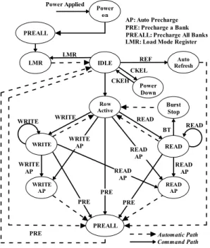
2) Finite State Machine (FSM)
Fig. 6 shows the finite state machine (FSM) of the external memory interface, which processes the DRAM access and generate the DRAM commands along with the consideration of the timing constraints while providing the minimal latency. The timing checker and the NOP counter are used to check the timing constraints of each state. The state register that records the status of each bank is used for the scheduling of read/write commands so as to minimize the number of cycles between commands. In addition, the operations of all the banks are controlled by one unified FSM instead of multiple FSMs such that the cost the memory controller is minimized.
C. Synchronization Buffer
The size of the synchronization buffer is critical to the efficiency of the DRAM access. A synchronization buffer of larger size allows multiple DRAM accesses to be optimized
jointly. For instance, if the synchronization buffer is designed in such a way that the data required for the decoding of a slice can be fetched in advanced, then one can schedule the data access of a slice according to the target addresses to minimize the row miss and thus increase the effective DRAM bandwidth. Apparently, the efficiency is gained at the cost of extra gate counts. Therefore, how to identify the size of the synchronization buffer that can provide the best trade-off between the efficiency of DRAM access and the hardware cost becomes one of the key issues for the memory sub-system.
TABLE I compares the cycle counts per macroblock (MB) when the synchronization buffer is designed at the levels of 4x4, 8x8, 16x16 (1 MB), and 32x16 (2 MBs). Note that the number is obtained based on the worst case assumption, in which the sub-pel interpolation of a 4x4 block requires the most input data, no redundant data are fetched for different blocks, and the input data are distributed in different banks.
As shown, smaller block size causes poor DRAM bandwidth utilization because of more DRAM active and precharge operations. Equivalently, for the same real-time requirement and clocking rate, the configuration with smaller
block size demands more DRAMs and wider AHB data bus. In TABLE I, when one DRAM is used, only the granularity of 2MBs can fulfill the real-time requirement when clocking at 162MHz, i.e., 660cycles/MB.
However, in H.264/AVC, designing for the worst case may not be the best policy since the worst case could only occur in an irrational sequence. Moreover, the bandwidth increase by using more DRAMs could be constrained by the limited pin counts. In Section VI, we show the performance of the proposed memory sub-system when the synchronization buffer is designed at different levels of granularity.
IV. CONSTANT-RATE BUMPING PROCESS
The bumping process in H.264/AVC manages the output of decoded pictures such that the output order conforms to the display order. Different from the prior video coding standards in which the decoder can output the decoded pictures according to the timestamp information in the picture or slice header, the NAL units of H.264/AVC do not contain any timing information. Thus, the bumping process defines the
Power Applied PREALL Power on LMR Row Active LMR
IDLE REF RefreshAuto CKEL CKEH Power Down READ READ AP WRITE WRITE AP PREALL READ BT READ READ AP PRE WRITE AP WRITE WRITE WRITE AP PRE PRE READ AP READ AP
PRE Automatic Path
Command Path
AP: Auto Precharge PRE: Precharge a Bank LMR: Load Mode Register PREALL: Precharge All Banks
Burst Stop
Fig. 6. The finite state machine designed for the mobile DDR SDRAM.
TABLE I
ANALYSIS OF THE DIFFERENT LEVELS OF GRANULARITIES BASED ON
THE WORST CASE ASSUMPTION
Granularity 4x4 8x8 1 MB 2 MB Sync. Buffer (Bits) 2160 5424 20160 40320 Cycles/MB (1 DRAM) 2096 940 745 454
Configuration for 1920x1080@30Hz
Number of DRAM (N) 8* 4 2 1
Cycles/MB (N DRAM) 1136 532 595 454 Bandwidth Utilization 7.3% 16.8% 28.1% 78.2%
AHB Bus (bits) 128 128 64 32
rules for ensuring correct output of decoded pictures. It should be noted that the output of a decoded picture does not necessarily imply the removal of the picture from the DPB. For a reference picture, it may still be kept in the DPB for temporal prediction while it is output for display.
A. Bumping Process in H.264/AVC
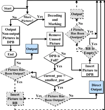
Fig. 7 shows the flow chart of the current bumping process in H.264/AVC. As shown, after the decoding of a picture, those in the DPB that are marked as unused for reference and have been output for display will be removed from the buffer. Then, the bumping process is enabled by checking whether the DPB has more space for the current picture. In case that the DPB is still fully occupied, the non-output picture in the DPB that has the smallest picture order count (POC) will be firstly considered for output unless the current picture has an even smaller POC and needs to be output directly. After the output of a decoded picture in the DPB, it will be further removed if it is no longer used for reference. However, it could happen that the picture just output for display still needs to be kept for reference. Thus, such a process must be repeated until space is found or the current picture is output.
Due to the iterative bumping behavior in the current algorithm, multiple decoded pictures could be output simultaneously while for some time instances none of the pictures are output. The irregular output rate of the bumping process causes extremely varying bandwidth during the DRAM access. The number of frame buffer in DRAM is double to regulate the burst of output. Thus, the maximum number of output pictures at a time is equal to DPB size plus one. In addition to the space of DPB, the regulation buffer is used for buffering the direct outputs that is not stored in the DPB. With a constant-rate bumping process, we can output one picture at a time without violating the output order conformance.
B. Proposed Constant-Rate Bumping Process
To provide a constant output rate and minimize the bandwidth variation for the DRAM access, an output regulation buffer is created in addition to the DPB. In particular, the bumping process in H.264/AVC may output all pictures in the DPB and the current decoding picture. Thus, a buffer with size being equal to the one of the DPB is allocated to regulate the burst of output. Fig. 8 shows the proposed constant-rate bumping algorithm using the regulation buffer. As highlighted by the gray blocks and the dotted lines, the major difference in contrast to the variable-rate bumping process is that there will be only 1 picture output for display after the decoding of a picture. As a result, when the DPB is still fully occupied after the output of a picture, the current picture will be stored in the regulation buffer. On the other hand, when space is available, the DPB keeps the current picture and the regulation buffer may output 1 picture according to the constraint on the output rate.
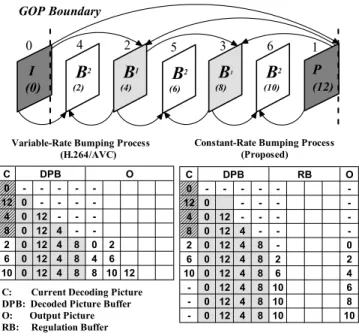
For better understanding, Fig. 9 uses an example to compare the two bumping processes, where the numbers in the parentheses indicate the display order, the number on the top of each picture denotes the coding order, and the arrowheads reveal the prediction structure with those pictures of gray color used for reference. According to the flow in Fig. 7, the variable-rate bumping process outputs 2 to 3 pictures when decoding the non-reference B pictures such as pictures 2, 6, and 10. Conversely, the proposed bumping process provides constant output rate while maintaining the conformance of output order.
Start Decoding and Marking Output Remove Unused Picture Output Non-output Pictures in DPB End Direct Output No Yes No DPB Is Full? current_poc < smallest_poc Insert Picture to DPB Yes Iterative Loop Yes No More Picture?
Fig. 7. The flow chart of the bumping process in H.264/AVC. The “smallest_poc” stands for the smallest picture order count (POC) among the non-output pictures in the DPB.
Start Decoding and Marking Output Remove Unused Picture Output Non-output Pictures in DPB End Direct Output No Yes No DPB is Full? current_poc < smallest_poc Insert Picture to DPB Yes Yes No Insert Picture to RB 1 Picture Has Been Output? 1 Picture Has Been Output? Yes No Yes No RB Is Empty? Output Yes No 1 Picture Has Been Ooutput? Yes No More Picture?
Fig. 8. The flow chart of the proposed constant-rate bumping process. The “smallest_poc” stands for the smallest picture order count (POC) among the non-output pictures in the DPB and the “RB” denotes the regulation buffer.
V. IMPLEMENTATION AND PLATFORM ASSEMBLY
In this section, we employ transaction level modeling technique to implement the proposed system architecture and assess the performance of the memory sub-system in combination with other modules. Particularly, the entire system is modeled at mixed levels of abstraction and simulated using CoWare ConvergenSCTM [8].
A. System Simulation with Mixed Levels of Abstraction System simulation with mixed levels of abstraction allows one to find the best trade-off between simulation speed and modeling accuracy. In this paper, the memory sub-system is of major concern and is thus modeled with every detail at register transfer level using Verilog. On the other hand, the remaining parts of the system are modeled at a higher level of abstraction, known as the transaction level, with SystemC [7] to gain faster simulation speed.
For the transaction level modeling, the interface between modules and the granularity for data exchange are defined. In addition, the functionalities within a module are described by a set of concurrent processes with annotated timing information. To synchronize the modules at different levels of abstraction, the data exchanges are trigged by calling the interface functions bound to the ports of a module and carried out by the implementation of the channels that connects the ports of different modules. Furthermore, within a module, the task modeling is accomplished by the evaluation of the task followed by N waiting cycles annotated from the associated hardware architecture as shown in Fig. 10.
B. Platform Creation
After the model creation, all the modules in the proposed H.264/AVC decoder are assembled and simulated on the Platform Architect of Coware’s ConvergenSCTM, as shown in
Fig. 11. Particularly, the external memory interface modeled in Verilog is instantiated in the SystemC-based platform by using a proxy module, which acts as a wrapper and deals with the signal exchange across the two different simulators. Compared with traditional system simulation at register transfer level, the transaction level modeling significantly reduce the design regression cycle while offering sufficient simulation accuracy.
VI. SIMULATION RESULTS
In this section, we use the platform created with CoWare ConvergenSCTM to statistically analyze the DRAM access
when the synchronization buffer is designed at different levels of granularities, including 4x4, 8x8, and 16x16. The analysis
1 5 3 6 0 4 2 I (0)
B
2 (2)B
1 (4)B
2 (6)B
1 (8)B
2 (10) P (12) GOP Boundary C DPB O 0 - - - - -12 0 - - - -4 0 12 - - -8 0 12 4 - -2 0 12 4 8 0 2 6 0 12 4 8 4 6 10 0 12 4 8 8 10 12 C DPB RB O 0 - - - - - -12 0 - - - -4 0 12 - - - -8 0 12 4 - - -2 0 12 4 8 - 0 6 0 12 4 8 2 2 10 0 12 4 8 6 4 - 0 12 4 8 10 6 - 0 12 4 8 10 8 - 0 12 4 8 10 10 C: Current Decoding PictureDPB: Decoded Picture Buffer O: Output Picture RB: Regulation Buffer
Variable-Rate Bumping Process (H.264/AVC)
Constant-Rate Bumping Process (Proposed)
Fig. 9. Example for comparing the variable-rate bumping process and the proposed constant-rate bumping process.
Behavior1
Write_if Behavior 2Write_if
Behavior 3 Write_if
Wait Wait Wait
Cycles of Task
Emit_if @ posedge clk Synchronization Event @ posedge clk Read_if (ping-pong index) Data and Control
S tag e 1 S tag e 2 St ag e 3
Stage 3 Stage 1 Stage 2 Stage 3
Notify Sync. by Sync. Channel Compute Wait Compute Wait Wait Compute Emit_if Wait Stage 1 Finite State Machine
Fig. 10. The SystemC implementation with the annotated timing.
Fig. 11. The proposed H.264/AVC decoder implemented by Platform Architect of CoWare ConvergenSCTM.
is conducted by deploying one external DRAM. To capture the characteristics for different scenarios, the testing sequences include 4 QCIF sequences (Stefan, Mobile, Table, Coastguard) and 4 HD sequences (Pedestrian, Rush_hour, Sunflower, and Station2.). Each sequence is further coded at low, medium, and high bit rates by using the Qp of 10, 28, and 45 respectively. In addition, to minimize the number of active and precharge operations, the data mapping in the external DRAM is based on the checkerboard arrangement as presented in Section III.
Fig. 12 shows the memory efficiency of motion compensation, which dominates the access of DRAM. As shown, the access of DRAM has higher efficiency when using larger block size. By firstly observing the block partition and motion vectors, we can prevent redundant data from transfer. Fig. 13 further shows the memory efficiency from the system perspective; that is, the DRAM access for the on-chip modules is simultaneously considered. Again, we have similar observation as in Fig. 12. However, the difference between the 8x8 and 16x16 is not significant at medium or low bit rates.
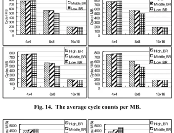
To evaluate the DRAM latency, Fig. 14 illustrates the average cycle counts for DRAM access per MB. Here, we consider all the data transfer for the on-chip modules. As expected, larger block size require less DRAM cycles because of higher memory efficiency. Moreover, as shown in Fig. 15,
larger block size also has less memory overhead due to less frequent active and precharge operations.
The efficiency of DRAM access also affects the power dissipation. Fig. 16 compares the estimated power dissipation for different block granularities according to the DRAM specification [6]. As shown, smaller granularity dissipates higher power due to more DRAM commands. Moreover, since each active or precharge command spends 7x power consumption than the read/write commands, larger block size, which has less active and precharge operations, is more efficient in terms of power dissipation.
From the experimental results, we obtain the conclusions as follows: (1) with one DRAM, only 2MBs granularity guarantees the design for worst case. However, (2) using 0 20 40 60 80 100 4x4 8x8 16x16 Ba nd w id th ef fic ien cy o f M C ( % ) High_BR Middle_BR Low BR 0 20 40 60 80 100 4x4 8x8 16x16 Ba nd w id th ef fic ien cy o f M C ( % ) High_BR Middle_BR Low BR 0 20 40 60 80 100 4x4 8x8 16x16 ba nd wi dt h ef fic ie nc y of M C (% ) High_BR Middle_BR Low BR 0 20 40 60 80 100 4x4 8x8 16x16 ba nd wi dt h ef fic ie nc y of M C (% ) High_BR Middle_BR Low BR
Fig. 12. The efficiency of DRAM access for motion compensation. The efficiency is defined as (# of data read from the external DRAM) / (actual data required for the motion compensation).
0 20 40 60 80 100 4x4 8x8 16x16 Ba nd wi dt h ef fic ie nc y of M C (% ) High_BR Middle_BR Low BR 0 20 40 60 80 100 4x4 8x8 16x16 Ba nd wi dt h ef fic ie nc y of M C (% ) High_BR Middle_BR Low BR 0 20 40 60 80 100 4x4 8x8 16x16 ba nd wi dt h ef fic ie nc y of M C (% ) High_BR Middle_BR Low BR 0 20 40 60 80 100 4x4 8x8 16x16 ba nd wi dt h ef fic ie nc y of M C (% ) High_BR Middle_BR Low BR
Fig. 13. The efficiency of DRAM access for the decoder. The efficiency is defined as (# of data read from the external DRAM) / (actual data required for the motion compensation).
0 100 200 300 400 500 600 700 800 4x4 8x8 16x16 Cy cl e / M B High_BR Middle_BR Low BR 0 100 200 300 400 500 600 700 800 4x4 8x8 16x16 Cy cl e / M B High_BR Middle_BR Low BR 0 100 200 300 400 500 600 700 800 4x4 8x8 16x16 Cy cl e / M B High_BR Middle_BR Low BR 0 100 200 300 400 500 600 700 800 4x4 8x8 16x16 Cy cl e / M B High_BR Middle_BR Low BR
Fig. 14. The average cycle counts per MB.
1500 2000 2500 3000 3500 4000 4500 5000 4x4 8x8 16x16 Tr an sf er re d da ta (B yt es / M B) High_BR Middle_BR Low BR 1500 2000 2500 3000 3500 4000 4500 5000 4x4 8x8 16x16 Tr an sf er re d da ta (B yt es / M B) High_BR Middle_BR Low BR 1500 2000 2500 3000 3500 4000 4500 5000 4x4 8x8 16x16 Tr an sf er re d da ta (B yt es / M B) High_BR Middle_BR Low BR 1500 2000 2500 3000 3500 4000 4500 5000 4x4 8x8 16x16 Tr an sf er re d da ta (B yt es / M B) High_BR Middle_BR Low BR
Fig. 15. The amount of data transfer.
0 1 2 3 4 5 4x4 8x8 16x16 Po we r ( m J / M B) High_BR Middle_BR Low BR 0 0.51 1.52 2.53 3.54 4.5 4x4 8x8 16x16 Po w er (m J / M B) High_BR Middle_BR Low BR 0 1 2 3 4 5 4x4 8x8 16x16 Po we r (m J / M B) High_BR Middle_BR Low BR 0 1 2 3 4 5 4x4 8x8 16x16 Po we r (m J / M B) High_BR Middle_BR Low BR
16x16 granularity with one DRAM is sufficient for the average case. Moreover, (3) using 8x8 granularity with one DRAM consumes more power while the synchronous buffer can be reduces. In addition, (4) using 4x4 granularity requires least internal buffer, but needs more external DRAMs to provide higher bandwidth. In summary, the synchronization buffer with larger block size has higher memory efficiency, and thus, less DRAM access cycles and power dissipation. However, the 8x8 granularity provides better trade-off among cost, efficiency, power, and real-time requirement.
VII. CONCLUSIONS
The intensive, irregular DRAM access in the H.264/AVC decoder makes the memory sub-system become the performance bottleneck for the real-time applications. Moreover, the variable-rate bumping process further complicates the management of decoded picture buffer. To tackle these issues, we propose an efficient memory sub-system and a constant-rate bumping process. Firstly, the memory interface is designed to optimize the issues of read/write commands and the auto-precharge function. Moreover, an interleaved data arrangement is proposed to reduce the probability of row miss. Secondly, a regulation buffer with size being equal to the decoded picture buffer is created to ensure a constant output rate of decoded pictures for any conformed prediction structures. Thirdly, a synchronization buffer at the granularity of 8x8 is used to maximize the DRAM bandwidth while minimizing the extra cost. From the system level simulation with transaction level modeling, the proposed schemes can achieve the decoding throughput of 1920x1080@30Hz while clocking at 162MHz.
REFERENCES
[1] ITU-T Rec. H.264 and ISO/IEC 14496-10 (MPEG4-AVC), .Advanced Video Coding for Generic Audiovisual Services,. v1, May, 2003; v2, Jan. 2004; v3, Sept. 2004; v4, July 2005
[2] H. Kim, and I. C. Park, “High-performance and low-power memory-interface architecture for video processing applications, ” IEEE Trans. Circuits and Systems for Video Technology, vol. 11, no 11,pp.1160– 1170, 2001.
[3] J. Zhu, L. Hou, R. Wang, C. Huang, and J. Li, “High performance synchronous DRAMs controller in H.264 HDTV decoder” in Proc. IEEE Int. Conf. Solid-state and Integrated Circuits Technology., vol. 3, pp.1621–1624, Beijing, China, Oct. 2004..
[4] R. Wang, J. Li, and C. Huang, “Motion Compensation Memory Access Optimization Strategies for H.264/AVC Decoder,” International Conference on Acoustics, Speech, and Signal Processing, vol. 5, pp. 97.100, 2005.
[5] S. I. Park, Y. Yongseok, and I. C. Park, “High performance memory mode control for HDTV decoders,” IEEE Trans. Consumer Electronics, vol.49, no.4, pp. 1348–1353, 2003.
[6] Mircron, http://www.micron.com.
[7] Open SystemC Initiative, SystemC Version 2.0 User’s Guide; www.systemc.org
[8] CoWare, “ConvergenSCTM,” http://www.coware.com
Chih-Hung Li was born in Taipei, Taiwan in 1979. He received the B.S. degree in Electronics Engineering from National Chiao-Tung University, Hsinchu, Taiwan, in 2001, where he is currently pursuing his PhD degree in the Institute of Electronics. His research interests include video transcoding, platform-based System-on-Chip design, system architecture modeling, and DRAM controller.
Wen-Hsiao Peng was born in Hsin-Chu, Taiwan, 1975. He received the B.S. and the M.S. degrees with highest distinction in electronics engineering from the National Chiao-Tung University, Taiwan in 1997 and 1999, respectively. In 2000, he joined Intel Microprocessor Research Laboratory, Santa Clara, U.S.A., where he developed the first real-time MPEG-4 FGS codec and demonstrated its application in a 3-D, peer-to-peer video conferencing. In 2002, he joined the institute of electronics of National Chiao-Tung University, Taiwan as a Ph.D candidate. He received the Ph.D degree in 2005 with the dissertation on “Scalable Video Coding – Advanced Fine Granularity Scalability”. Since 2003, he has actively participated in ISO's Moving Picture Expert Group (MPEG) digital video coding standardization process and contributed to the development of MPEG-4 Part 10 AVC Amd.3 scalable video coding (SVC) standard. His major research interests include video coding, video codec optimization, and platform-based architecture design. He has published over 30+ technical papers in the field of video and signal processing.
Tihao Chiang (S’91–M’95–SM’99) was born in Chia-Yi, Taiwan, R.O.C., in 1965. He received the B.S. degree in electrical engineering from the National Taiwan University, Taipei, in 1987, the M.S. degree in electrical engineering in 1991 and the Ph.D. degree in electrical engineering in 1995, both from Columbia University, New York. In 1995, he joined the David Sarnoff Research Center, Princeton, NJ, as a Member of Technical Staff, and was later promoted to Technology Leader and Program Manager. While at Sarnoff, he led a team of researchers and developed an optimized MPEG-2 software encoder. In September 1999, he joined the faculty at National Chiao-Tung University, Hsinchu, Taiwan. Since 1992, he has actively participated in ISO’s Moving Picture Experts Group (MPEG) digital video coding standardization process with particular focus on the scalability/compatibility issue. He is currently the co-editor of Part 7 of the MPEG-4 Committee and has made more than 90 contributions to the MPEG Committee over the past ten years. His main research interests are compatible/scalable video compression, stereoscopic video coding, and motion estimation. He holds 13 U.S. patents and 30 European and worldwide patents and has published over 50 technical journal and conference papers in the field of video and signal processing.
Dr. Chiang was a co-recipient of the 2001 Best Paper Award from the IEEE TRANSACTIONS ON CIRCUITS AND SYSTEMS FOR VIDEO TECHNOLOGY. For his work in the encoder and MPEG-4 areas, he received two Sarnoff achievement awards and three Sarnoff team awards.