Abstract—This paper presents, for the first time, a directional coupler that allows for arbitrary power division ratios as well as arbitrary phase differences at dual frequencies of interest. Explicit design equations in terms of dual-band power-dividing ratios and phase differences will be given here and were derived based on the even- and odd-mode decomposition analysis. To illustrate the de-sign procedure, examples will be provided and the relevant studies on the coupler’s electrical parameters for a wide range of dual-band specifications and frequency ratios were conducted, by which the graphical solutions can be readily used as the further design tool. In addition, the resulting operational bandwidths are included and discussed for completeness. To validate our idea, four cou-pler prototypes were carried out according to the given guidelines. Excellent agreement is obtained between the measured and full-wave calculated results. The functional versatility of the proposed simple structure is well suited to applications in dual-band inte-grated modules, such as the beam-forming networks, for both loss and size reduction.
Index Terms—Arbitrary phase differences, arbitrary power di-vision ratios, directional coupler, dual bands.
I. INTRODUCTION
D
IRECTIONAL couplers are one of the most essential building components in the modern communication systems. In this respect, coupler developments in various as-pects of applications have been extensively explored over the decades. In general, the improved functionality or performance with size reduction [1], [2], dual-band or multi-band operation [3]–[9], or bandwidth enhancement [10] is of great interest. On the other hand, the practicability of unequal power division between output ports renders a useful solution for intentional power distribution or power compensation in antenna/circuit feeding networks [11]–[15]. Additionally, the coupler design that features filtering and power splitting/combining in a single unit can reduce the number of circuit components and thus occupy less space [16], [17].Recently, the coupler’s ability to produce an arbitrary phase difference between the through and coupled ports [18], and Manuscript received May 20, 2014; revised September 08, 2014; accepted October 12, 2014. Date of publication October 30, 2014; date of current version December 02, 2014. This work was supported in part by the Ministry of Science and Technology of Taiwan under Grant MOST 103-2221-E-009-032.
P.-L. Chi is with the Department of Electrical and Computer Engineering, Na-tional Chiao Tung University, Hsinchu 300, Taiwan (e-mail: peilingchi@nctu. edu.tw).
K.-L. Ho was with the Department of Electrical and Computer Engineering, National Chiao Tung University, Hsinchu 300, Taiwan. He is now with Garmin Inc., New Taipei City 221, Taiwan.
Color versions of one or more of the figures in this paper are available online at http://ieeexplore.ieee.org.
Digital Object Identifier 10.1109/TMTT.2014.2364218
moreover, to combine the flexibility of an arbitrary power division ratio [19]–[23] finds promising applications in many fields. For example, the reflectometer is able to attain optimum design condition by use of hybrid couplers with nonstandard phase differences [24], [25]. Besides, the phase shifters may be removed in conventional beam-forming networks, such as in the Butler matrix [26], [27], where the phase shift can be incorporated into the developed couplers or crossovers with arbitrary phase differences or output phases [22]. In [18], the coupler with arbitrary phase differences was proposed while its fixed (3 dB) power division limits the usage applications. In the follow-up comments on the same coupler, the capability of arbitrary coupling level was supplemented [19]. However, the phase difference concerned herein [19] only ranges from 0 to 90 for the same port excitation, which, in reality, can be extended to an arbitrary value between 0 –360 and will be considered in this presented work. Similarly, the coupler structure in [20] fails to discuss the feasibility of any phase difference other than the value between 0 –90 . In addition, in order to realize arbitrary phase differences, a patterned ground plane is needed in the circular sector patch coupler where a systematic design approach is not available [21]. The use of lumped elements contributes to considerable size reduction, but prevents the coupler prototype from high-frequency appli-cations [22], [23]. Note that, so far in the literature, the coupler functionality having an arbitrary power division and arbitrary phase difference is limited to single-band operation and less effort was made on coupler development with such capability at dual frequencies.
To this end, a single-layer and simple coupler structure is pre-sented and developed in this paper. The even- and odd-mode decomposition technique was applied for coupler analysis. In order to perform dual-band operation, the network was used to design the constituent transmission lines of arbitrary impedance and phase variations in dual bands of interest. The closed-form design equations will be given in terms of the power division ratios and phase differences in dual bands. Furthermore, the coupler’s ability to realize nonstandard phase differences de-fined between 0 –360 (not including 0 /360 and 180 ) will be emphasized and discussed in detail. This paper is organized as follows. In Sections II-A and II-B, the operating principle as well as the dual-band realization of the proposed coupler will be presented where the explicit formulas and a system-atic design guideline are included to attempt arbitrary power division ratios and arbitrary phase differences in dual bands. Later, examples are given to illustrate the design procedure and the various investigations on the coupler’s electrical parameters and operational bandwidths versus a wide range of dual-band 0018-9480 © 2014 IEEE. Personal use is permitted, but republication/redistribution requires IEEE permission.
Fig. 1. Schematic representation of the proposed coupler with arbitrary power division ratios and phase differences at dual frequencies.
specifications were conducted in Section II-C. In Section III, four dual-band coupler prototypes were developed, fabricated, and characterized by experiments. The experimental results, in-cluding the magnitude and phase responses, will be carefully compared to the full-wave calculated counterparts. Finally, a conclusion is drawn in Section IV.
II. ANALYSIS AND IMPLEMENTATION OF THEDUAL-BANDCOUPLER
A. Operating Principle
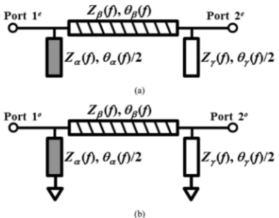
The schematic illustration of the proposed coupler with arbi-trary power division ratios and phase differences in dual bands is shown in Fig. 1. The presented coupler is composed of four branch-line elements, including a transmission-line element of impedance and electrical length between ports 1 and 4, a transmission-line element of impedance and electrical length between ports 2 and 3, and a pair of iden-tical line elements of impedance and electrical length . Thus, as can be seen, the structure is symmetric across the midplane and can be analyzed by the even- and odd-mode decomposition technique with the half circuits shown in Fig. 2. Note that each transmission-line element here is responsible for dual-band (designated as and ) implementation, which re-quires that both of its impedance and electrical length be flexibly engineered at dual frequencies of interest. Thus, the impedance and phase ( , or ) are functions of frequency and the network will be applied for developing such a line proto-type. This realization will be detailed in Section II-B. Without loss of generality, if port 1 is designated as the input port, ports 3 and 4 are the outputs of the coupled and through arms, re-spectively, while port 2 will be the isolated port. Therefore, the power division ratio and the output phase difference are defined as the power-split difference and phase difference, respectively, between ports 4 and 3 when port 1 is excited,
(1) (2) As addressed previously, the proposed coupler is intended to realize arbitrary output parameters and in dual bands of
Fig. 2. (a) Even-mode and (b) odd-mode half circuits for analysis of the pro-posed coupler.
interest, and for design purposes, the mathematical relations in terms of the coupler’s electrical parameters will be derived here-after.
Referring to Fig. 2, the transmission characteristics of the even or odd mode can be conveniently computed by using the transmission matrix, which is the product of the ma-trices representing the individual sub-circuits
(3a)
(3b)
(3c) where or stands for the even or odd mode, respectively. Note that the frequency dependence is omitted for simplicity, but will not affect the outcome conditions required for proper dual-band operation. Once the parameters of the two-port even-and odd-mode networks are obtained, the corresponding reflec-tion and transmission coefficients can be readily calculated by conversion between network parameters [28]. Fi-nally, the -parameters of the coupler are related to the even-and odd-mode reflection even-and transmission coefficients as fol-lows:
(4a) (4b) (4c) (4d)
According to (5), the parameters of the even- and odd-mode half circuits can be related as follows:
(6a) (6b) (6c) (6d) where is the port (reference) impedance. In particular, from (6c), the following equation can be derived:
(7) Thus, if is chosen equal to , the phase relation between
and can be deduced as follows:
if (8)
where is a non-negative integer . Note that, the other phase solution is disregarded in that the resulting phase difference will reduce to only odd mul-tiples of 90 after a further analysis and thus is not considered here for arbitrary phase engineering. Next, the phase can be solved from (6d) with (8),
where (9)
For size reduction, is preferred and will be chosen for phase implementation with . On the other hand, for the realization with , it can be shown that will be needed. In addition, the impedance can be related to by using (6b) in conjunction with the results in (8) and (9),
(10)
It can be verified that (6a) still holds with the solutions given in (8)–(10). Thus, the power division ratio and the phase dif-ference , which are already defined in (1) and (2), can be ex-pressed in terms of the above-mentioned parameters as follows: (11) (12) (14) if if (15) if if (16) if if (17)
Note that, for reduced length and better bandwidth, the phase values are chosen as small as possible. Given the power division ratio and phase difference at either operating frequency or , the corresponding impedances and electrical lengths of the three transmission-line elements in Fig. 1 can be obtained ac-cording to (13)–(17). Furthermore, by inspection of (15)–(17), several important observations can be found as follows.
1) Compared to the case with a phase difference , the values and are interchanged when designing the phase dif-ference . Thus, if a phase difference is defined as , it can be easily shown that . In other words, in Fig. 1, the phase differences and measured at ports 1 and 2, respectively, are supplementary angles. In [18] and [19], such a particular phase relation was illustrated by calculated/experimental results, but an-alytical explanation is not available therein.
2) The electrical parameters for the case with a phase differ-ence are identical to those of the counterpart having the same power division ratio and phase differ-ence , except that the electrical length is increased
by 180 .
3) The proposed structure is unable to realize the in-phase ( or 360 ) or antiphase (180 ) phase difference given that port 2 is the isolated port when port 1 is excited. Instead, if port 3 is defined as the isolated port, such a phase difference is feasible between ports 2 and 4, as was presented in [15].
B. Dual-Band Implementation
As can be observed from (13) and (14), the impedance of each transmission-line element in the coupler may be different accordingly at dual frequencies to fulfill arbitrary power divi-sion ratios and phase differences. Thus, the network is applied
Fig. 3. network for implementing a transmission-line element of effective impedance and electrical length .
to implement each line element in Fig. 1. As shown in Fig. 3, the network consists of a host transmission line of character-istic impedance and electrical length (evaluated at the lower frequency ), and two identical open stubs loaded at both ends. The parameter represents the admittance of the open stubs. Thus, at operational frequencies and , the
parameters of the original line element must equate to those of the network as follows:
(18a)
(18b)
where . Note that , and
represent the prior known parameters for any line elements in the coupler and can be readily obtained from (13)–(17) as soon
as the values of and are specified.
Thus, , and can be solved as follows:
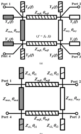
(19) (20) (21) (22) By replacing each transmission-line element in Fig. 1 with the corresponding network, the proposed dual-band coupler is il-lustrated in Fig. 4(a) where the previously calculated parameters
Fig. 4. (a) Configuration and (b) realized prototype of the proposed dual-band coupler based on the networks. All electrical lengths are evaluated at .
and ( , or ) are indicated. To facil-itate fabrication, each pair of loaded stubs at the same vertex was implemented as a single open stub, as shown in Fig. 4(b). Thus, the realized coupler prototype comprises two kinds of open stubs with characteristic impedances and and elec-trical lengths and , and can be determined by and
in (21) and (22) as follows:
(23) (24) (25) (26)
C. Examples and Design Procedure
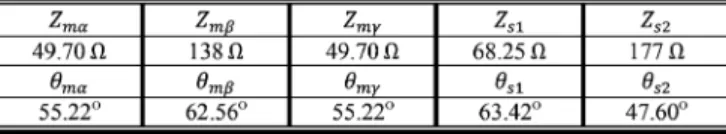
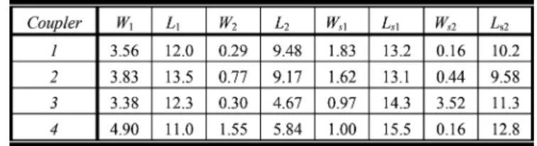
Having formulated coupler design in the previous sections, two examples are given here for demonstration purposes. The first coupler is designed at GHz and GHz (the
frequency ratio ) with
and . According to the
specifica-tion, Table I gives the corresponding dual-band parameters for the transmission-line elements in Fig. 1 using (13)–(17). Sub-sequently, by resorting to (19)–(26) with the data in Table I, the
TABLE II
CIRCUITPARAMETERS FOR THEPROPOSEDDUAL-BAND
COUPLERWITHSPECIFICATIONSGIVEN IN
TABLEI (ALLELECTRICALLENGTHS AREEVALUATED AT2.4 GHz)
TABLE III
CALCULATEDPARAMETERS FOR THETRANSMISSION-LINEELEMENTS IN THE
COUPLERGIVEN THEDIVISIONRATIOS ,
ANDPHASEDIFFERENCES
TABLE IV
CIRCUITPARAMETERS FOR THEPROPOSEDDUAL-BAND
COUPLERWITHSPECIFICATIONSGIVEN INTABLEIII (ALL
ELECTRICALLENGTHS AREEVALUATED AT2.4 GHz)
electrical parameters for the realized prototype in Fig. 4(b) can be obtained and are given in Table II. Similarly, the second cou-pler is operated at 2.4 and 5.2 GHz with
and . Tables III and IV present the
calculated results. In particular, since and
, by (19) and (20), it can be shown that and , as are seen in Tables II and IV. Additionally, in Tables I and III, the impedance in either case is notably higher than the impedance or , and is resulted from the
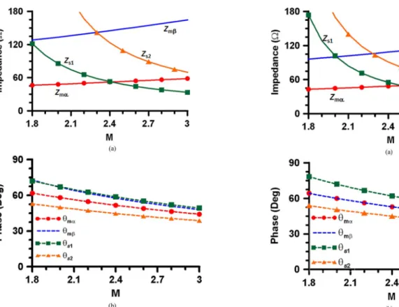
Fig. 5. (a) Host-line impedances, (b) stub-line impedances, and (c) host-line and stub-line electrical lengths against the ratio when
GHz and GHz. Three phase cases cor-responding to , and are illustrated by the solid curve, long dashed curve, and short dashed curve, respectively. The phase solutions for , and are represented by the curves with circle symbol, no symbol, square symbol, and triangle symbol, respectively.
high power division ratios specified in dual bands. By inspec-tion of (13) and (14), when the power ratio is large at a fre-quency, the impedance will increase accordingly and or will approach , typically 50 . As a consequence, by (20), the host line impedance in the network is usu-ally higher than the counterpart or . This inference can be validated from the diagrams in Fig. 5 where the im-pedances of the host lines as well as the open stubs are con-sidered with respect to the ratio when is fixed as 4. In this study, the frequency ratio . Note that three dual-band phase differences of
, and (60 , 75 ) are considered and illus-trated here. From Fig. 5(a), it can be observed that under consideration increases with the power division ratio
Fig. 6. (a) Impedances and (b) phases of the host lines and stub lines against
the frequency ratio when , and
.
for all cases while remains relatively constant around 50 . Furthermore, as the power ratio increases, in Fig. 5(b) the impedance of the open stub is remark-ably increased, which then determines the attainable power di-vision ratio for the proposed dual-band coupler based on the networks. For the prototype built on a RO4003C substrate of thickness 1.5 mm and of dielectric constant 3.38, the max-imum achievable impedance is about 180 for a 0.1-mm line width. Thus, the maximum impedance scale is limited to 180 throughout this paper to better clarify the feasible power and phase applications or the attainable frequency ratio in the dual-band scheme. Based on the results shown in Fig. 5(b), the max-imum realizable power division ratio is about 1.13 4, 1.75 4, and 2.0 4, respectively, for , and . The corresponding phase solutions for the host and stub lines are shown in Fig. 5(c). From Fig. 5(c), while less varia-tion is observed for the electrical length , the phase is gradually increased against the ratio of dual-band power di-visions, indicating that an increased coupler size, defined as the area enclosed by the host lines of and , is needed. Furthermore, when the phase varies from
to , both and are increased and this
re-sults in a larger footprint. Note that the impedance and phase values of the examples presented in Tables II and IV can be
ob-tained from Fig. 5 for and
, respectively.
On the other hand, the variations of the coupler’s electrical parameters versus the frequency ratio , with a variation step of 0.1, are investigated. Figs. 6 and 7 show the calculated
Fig. 7. (a) Impedances and (b) phases of the host lines and stub lines against
the frequency ratio when , and
.
results for
and for ,
respectively. It can be observed that as increases, the stub impedances and all electrical lengths are reduced, except the host-line impedances. Particularly, as becomes small, the stub impedance increases rapidly (as compared to ) and thus predominates the minimum attainable frequency ratio of dual-band operation based on the proposed architecture. From Figs. 6 and 7, it can be read that the minimum achievable ratio is about 2.2 and 2.0, respectively, for the first and second cases. Thus, the minimum obtainable dual-frequency separa-tion is varied from case to case and is determined by particular realizations of power ratios and phase differences. According to the above observations, to improve design flexibility of the dual-band coupler in terms of arbitrary operational fre-quencies or closer band separation, arbitrary power divisions, and phase differences, some auxiliary techniques that enable microstrip lines to be realized with high impedance can be applied at the expense of fabrication complexity such as the microstrip line with the defected ground structure [29] and the surface-mount inductor-loaded line section [30]. Furthermore, the fractional bandwidths in the respective bands and in correspondence with the case shown in Fig. 6 are illustrated in Fig. 8(a). The fractional bandwidth is defined as a frequency range where the return loss and isolation are better than 15 dB ( dB), the amplitude imbalance is less than 1 dB ( dB), and the phase imbalance is less than 10
. On the average, the fractional bandwidths are rel-atively constant over the frequency ratio in two operational
Fig. 8. (a) Fractional bandwidths against the frequency ratio . The dual-band
specification is as follows: , and
. The lower frequency was designated as 1 GHz. (b) Frac-tional bandwidths against the ratio when
GHz and GHz.
TABLE V
DUAL-BAND[ GHzAND GHz/5.8 GHz (FORCOUPLER3 ONLY)] SPECIFICATIONS FOR THEFOURFABRICATEDCOUPLERS
bands. In addition, the fractional bandwidths versus the ratio , corresponding to the case study in Fig. 5, are calculated and shown in Fig. 8(b). For the bandwidths centered at , it is seen that the bandwidths drop considerably with the ratio . Furthermore, it is interesting to note that a tradeoff exists for bandwidth performance between the three phase cases. In other words, the case with has the wider bandwidth at while having the narrowest bandwidth in its second band among the three. The reverse situation can be found for the case with .
In short, the design guidelines for the proposed dual-band coupler are summarized as follows.
Step 1) Use (13)–(17) to determine the impedances and , and the electrical lengths , and of the transmission-line elements at either frequency once the power division ratios and , and phase differences and are specified.
Fig. 9. Physical layout of the proposed coupler with arbitrary power division ratios and phase differences at dual frequencies. The coupler is symmetric across the horizontal midplane.
Fig. 10. Photograph of the fabricated dual-band coupler 1. TABLE VI
DIMENSIONS OF THEFOUR FABRICATEDCOUPLERS. ALLUNITSARE INMILLIMETERS
Step 2) Based on the values in Step 1, use (19)–(26) to obtain electrical parameters of the coupler prototype using the networks, including the host/stub-line
imped-ances , and , and host/
stub-line electrical lengths
and .
Step 3) In consideration of the coupler performance, choose appropriate phase solutions. To this end, shorter length is preferred for bandwidth enhancement and size reduction.
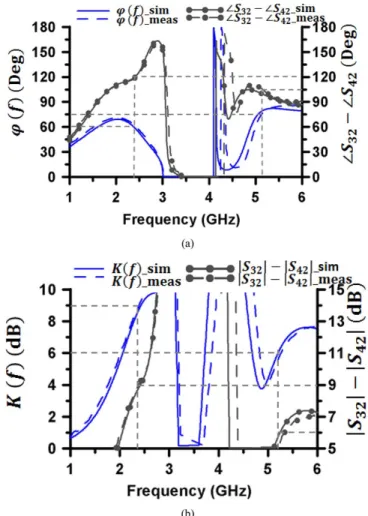
III. EXPERIMENTAL ANDFULL-WAVECALCULATEDRESULTS To validate the feasibility of the proposed design concept, four coupler prototypes with prescribed power divisions and phase differences in dual bands were developed, fabricated, and characterized. The dual-band specification for each realization is given in Table V. As can be seen, the presented examples of a variety of power division ratios and phase differences were carried out here. All dual-band couplers were designed at 2.4 and 5.2 GHz, except for coupler 3, which operates at 2.4 and
Fig. 11. Measured (dashed lines) and simulated (solid lines) -parameters of the coupler 1. (a) -parameters obtained when port 1 is the input port. (b) -parameters obtained when port 2 is the input port.
5.8 GHz. All couplers were developed on the RO4003C sub-strates of thickness mm (60 mil) and of dielectric con-stant . The physical layout of the proposed dual-band coupler is shown in Fig. 9. Note that the coupler is symmetric across the horizontal midplane. When referring to Fig. 4(b), the horizontal lines with width correspond to the host lines of characteristic impedance while the vertical lines with width represent the host lines of impedance . In addition, the stub lines with widths and are the open stubs of impedances and , respectively. Note that, though not considered in this presented work, size reduction of the proposed dual-band coupler may be achieved by prop-erly folding the host and stub lines [8], configuring the stubs in the area enclosed by the host lines [11], or designing the stepped-impedance host lines [11]. The photograph of the cou-pler 1 is shown in Fig. 10 and the corresponding physical di-mensions, along with those for the other three couplers, can be referred to Table VI. The measured and simulated -parameters of the coupler 1 are shown in Fig. 11 and are in excellent agree-ment. The full-wave simulation was carried out in the High Fre-quency Structure Simulator (HFSS). From Fig. 11, dual-band characteristics at 2.4 and 5.2 GHz are obtained. Furthermore, the experimental results of the power division ratio as well as the phase difference are depicted in Fig. 12. It can be ob-served that the power division ratios of (9 dB) and
(6 dB), and the phase differences of
Fig. 12. Measured and simulated: (a) phase differences and (b) power division ratios of coupler 1. The curves without and with the circle symbols represent the results obtained when the input ports are ports 1 and 2, respectively.
and are achieved as designed. Moreover, the mea-sured power division ratio and the phase difference with port 2 being the input port are included for validation purpose. From Fig. 12(a), it is verified that the sum of
the phase difference and is 180 at
either frequency, as was explained previously. Furthermore, the power division ratios (the right -axis) in Fig. 12(b) are 9 dB at 2.4 GHz and 6 dB at 5.2 GHz, which agree with the results obtained for at the respective frequencies. For better clarity, the detailed coupler performance, including the return loss , isolation , power division ratio
, phase difference , and
the corresponding bandwidths, are summarized and given in Table VII. Note that, compared to other results, the measured bandwidths at for the coupler 4 are, on the average, much smaller and can be attributed to the phase realization
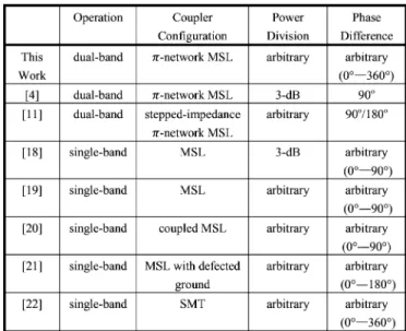
. Similar observation is found in Fig. 8(b) where the band-widths in the second band for are smaller than the bandwidths for and 75 . Nevertheless, the feasi-bility of the proposed design approach for the dual-band coupler prototype with arbitrary power division ratios and phase differ-ences is verified by the experimental results. Moreover, all the relevant works are compared in Table VIII where the coupler’s ability to afford dual- or multi-band operation, the circuit config-uration to facilitate coupler implementation, and the functional
Fig. 13. Simulated results for: (a) power division ratios and (b) phase
differ-ences for four coupler designs with , , , and
, respectively, and (9 dB) for all cases. The couplers
were designed at GHz and GHz.
flexibility to allow for arbitrary power divisions and arbitrary phase differences defined from 0 to 360 between the outputs are all taken into consideration. Note that in terms of the cou-pler configuration, similar structures can be found in [4] and [11] where the -network and the stepped-impedance -net-work were, respectively, utilized for compact and dual-band operation. On the other hand, due to the versatile power and phase applications, the -network in this work is mainly ap-plied for flexibly fulfilling power and phase requirements at dual frequencies of interest. In particular, compared to prior works,
TABLE VIII
PERFORMANCECOMPARISON FOR THEPROPOSED ANDREFERENCECOUPLERS
this presented coupler is the first realization of a dual-band pro-totype that attempts both arbitrary power divisions and phase differences. Furthermore, explicit design equations for a non-standard phase difference ranging from 0 to 360 (not appli-cable to the phases 0 /360 and 180 ) are provided for the pro-posed structure while most of references consider or discuss a limited phase-difference realization, such as from 0 to 90 or from 0 to 180 . To demonstrate the practicability of arbi-trary phase difference within 360 based on the presented de-sign guidelines, Fig. 13 shows the simulated results of four cou-pler prototypes with different phase differences 60 , 120 , 240 , and 300 and identical power division ratios
at GHz and GHz.
For each coupler, the division ratios of 9 dB as well as iden-tical phase differences (60 –300 ) in dual bands were obtained as designed. Note that according to (13) and (14), this presented coupler is unable to realize a phase difference (360 ) and between ports 3 and 4 (see Fig. 1). A further anal-ysis shows that the in-phase or antiphase phase difference can be fulfilled between ports 2 and 4 if ports 1 and 3 are designated as the input and isolated ports, respectively. In [21], to realize the 0 /180 phase differences, different output pairs were used. Nevertheless, it is clear that this work presents, for the first time,
a single-layer structure that exhibits greater design flexibility of the power divisions and phase differences engineering at dual frequencies of interest.
IV. CONCLUSION
In this paper, the analysis and design of a coupler prototype that allows for arbitrary power divisions and phase differences in dual bands are carried out for the first time and discussed in details. This coupler renders a simple structure with increased functionality such as the dual-band operation and an extended range of phase difference engineering. Good agreement is ob-tained between the experimental and calculated results.
REFERENCES
[1] D. I. Kim and G.-S. Yang, “Design of new hybrid-ring directional cou-pler using or sections,” IEEE Trans. Microw. Theory Techn., vol. 39, no. 10, pp. 1779–1784, Oct. 1991.
[2] H. Okabe, C. Caloz, and T. Itoh, “A compact enhanced-bandwidth hybrid ring using an artificial lumped-element left-handed transmis-sion-line section,” IEEE Trans. Microw. Theory Techn., vol. 52, no. 3, pp. 798–804, Mar. 2004.
[3] L. K. Yeung, “A compact dual-band 90 coupler with coupled-line sections,” IEEE Trans. Microw. Theory Techn., vol. 59, no. 9, pp. 2227–2232, Sep. 2011.
[4] K.-K. M. Cheng and F.-L. Wong, “A novel approach to the design and implementation of dual-band compact planar 90 branch-line coupler,”
IEEE Trans. Microw. Theory Techn., vol. 52, no. 11, pp. 2458–2463,
Nov. 2004.
[5] S. Y. Zheng, S. H. Yeung, W. S. Chan, K. F. Man, S. H. Leung, and Q. Xue, “Dual-band rectangular patch hybrid coupler,” IEEE Trans.
Microw. Theory Techn., vol. 56, no. 7, pp. 1721–1728, Jul. 2008.
[6] M.-J. Park and B. Lee, “Dual-band, cross coupled branch line coupler,”
IEEE Microw. Wireless Compon. Lett., vol. 15, no. 10, pp. 655–657,
Oct. 2005.
[7] P.-L. Chi and T. Itoh, “Miniaturized dual-band directional couplers using composite right/left-handed transmission structures and their ap-plications in beam pattern diversity systems,” IEEE Trans. Microw.
Theory Techn., vol. 57, no. 5, pp. 1207–1215, May 2009.
[8] F. Lin, Q.-X. Chu, and Z. Lin, “A novel tri-band branch-line coupler with three controllable operating frequencies,” IEEE Microw. Wireless
Compon. Lett., vol. 20, no. 12, pp. 666–668, Dec. 2010.
[9] C.-W. Tang and M.-G. Chen, “Design of multipassband microstrip branch-line couplers with open stubs,” IEEE Trans. Microw. Theory
Techn., vol. 57, no. 1, pp. 196–204, Jan. 2009.
[10] L. Chiu and Q. Xue, “Investigation of a wideband 90 hybrid coupler with an arbitrary coupling level,” IEEE Trans. Microw. Theory Techn., vol. 58, no. 4, pp. 1022–1029, Apr. 2010.
[11] C.-L. Hsu, J.-T. Kuo, and C.-W. Chang, “Miniaturized dual-band hy-brid couplers with arbitrary power division ratios,” IEEE Trans.
Mi-crow. Theory Techn., vol. 57, no. 1, pp. 149–156, Jan. 2009.
[12] X. Wang, W.-Y. Yin, and K.-L. Wu, “A dual-band coupled-line coupler with an arbitrary coupling coefficient,” IEEE Trans. Microw. Theory
Techn., vol. 60, no. 4, pp. 945–951, Apr. 2012.
[13] P.-L. Chi, “Miniaturized ring coupler with arbitrary power divisions based on the composite right/left-handed transmission lines,” IEEE
Mi-crow. Wireless Compon. Lett., vol. 22, no. 4, pp. 170–172, Apr. 2012.
[14] K.-L. Ho and P.-L. Chi, “Miniaturized and large-division-ratio ring coupler using novel transmission-line elements,” IEEE Microw.
Wire-less Compon. Lett., vol. 24, no. 1, pp. 35–37, Jan. 2014.
[15] M.-J. Park and B. Lee, “Design of ring couplers for arbitrary power division with 50 lines,” IEEE Microw. Wireless Compon. Lett., vol. 21, no. 4, pp. 185–187, Apr. 2011.
[16] C.-K. Lin and S.-J. Chung, “A compact filtering 180 hybrid,” IEEE
Trans. Microw. Theory Techn., vol. 59, no. 12, pp. 3030–3036, Dec.
2011.
[17] F. Lin, Q.-X. Chu, and S. W. Wong, “Design of dual-band filtering quadrature coupler using and resonators,” IEEE Microw.
Wireless Compon. Lett., vol. 22, no. 11, pp. 565–567, Nov. 2012.
[18] Y. S. Wong, S. Y. Zheng, and W. S. Chan, “Quasi-arbitrary phase-difference hybrid coupler,” IEEE Trans. Microw. Theory Techn., vol. 60, no. 6, pp. 1530–1539, Jun. 2012.
[19] Y. Wu, J. Shen, and Y. Liu, “Comments on ‘quasi-arbitrary phase-difference hybrid coupler’,” IEEE Trans. Microw. Theory Techn., vol. 61, no. 4, pp. 1725–1727, Apr. 2013.
[20] Y. Wu, J. Shen, Y. Liu, S.-W. Leung, and Q. Xue, “Miniaturized ar-bitrary phase-difference couplers for arar-bitrary coupling coefficients,”
IEEE Trans. Microw. Theory Techn., vol. 61, no. 6, pp. 2317–2324,
Jun. 2013.
[21] S. Y. Zheng, J. H. Deng, Y. M. Pan, and W. S. Chan, “Circular sector patch hybrid coupler with an arbitrary coupling coefficient and phase difference,” IEEE Trans. Microw. Theory Techn., vol. 61, no. 5, pp. 1781–1792, May 2013.
[22] E. Gandini, M. Ettorre, R. Sauleau, and A. Grbic, “A lumped-element unit cell for beam-forming networks and its application to a miniatur-ized Butler matrix,” IEEE Trans. Microw. Theory Techn., vol. 61, no. 4, pp. 1477–1487, Apr. 2013.
[23] E. Gandini, M. Ettorre, R. Sauleau, and A. Grbic, “A lumped-element directional coupler with arbitrary output amplitude and phase distribu-tions,” in IEEE MTT-S Int. Microw. Symp. Dig., Jun. 2012, pp. 1–3. [24] J. J. Yao and S. P. Yeo, “Six-port reflectometer based on modified
hy-brid couplers,” IEEE Trans. Microw. Theory Techn., vol. 56, no. 2, pp. 493–498, Feb. 2008.
[25] J. J. Yao, Y. Chen, and S. P. Yeo, “Modifying hybrid coupler design to enhance six-port reflectometer performance,” in Proc. Eur. Microw.
Conf., Oct. 2005, pp. 256–259.
[26] C.-W. Wang, T.-G. Ma, and C.-F. Yang, “A new planar artificial trans-mission line and its applications to a miniaturized Butler matrix,” IEEE
Trans. Microw. Theory Techn., vol. 55, no. 12, pp. 2792–2801, Dec.
2007.
[27] C.-C. Chang, T.-Y. Chin, J.-C. Wu, and S.-F. Chang, “Novel design of a 2.5-GHz fully integrated CMOS Butler matrix for smart-antenna systems,” IEEE Trans. Microw. Theory Techn., vol. 56, no. 8, pp. 1757–1763, Aug. 2008.
[28] D. M. Pozar, Microwave Engineering. New York, NY, USA: Wiley, 2005.
[29] J.-S. Lim, S.-W. Lee, C.-S. Kim, J.-S. Park, D. Ahn, and S. Nam, “A 4:1 unequal Wilkinson power divider,” IEEE Microw. Wireless Compon.
Lett., vol. 11, no. 3, pp. 124–126, Mar. 2001.
[30] H.-R. Ahn and S. Nam, “Wideband microstrip coupled-line ring hy-brids for high power-division ratios,” IEEE Trans. Microw. Theory
Techn., vol. 61, no. 5, pp. 1768–1780, May 2013.
Pei-Ling Chi (S’08–M’11) received the B.S. and
M.S. degrees in communication engineering from National Chiao Tung University (NCTU), Hsinchu, Taiwan, in 2004 and 2006, respectively, and the Ph.D. degree in electrical engineering from the University of California at Los Angeles (UCLA), Los Angeles, CA, USA, in 2011.
Since 2011, she has been with the National Chiao Tung University, as an Assistant Professor of elec-trical and computer engineering. She holds several U.S. and international patents in the area of the left-handed metamaterials. Her research interests include the analysis and design of left-handed metamaterial circuits, implementation of microwave components and integrated systems, and development of millimeter-wave/terahertz antennas and communications.
Dr. Chi was the recipient of the Research Creativity Award from the National Science Council, Taiwan, in 2004.
Kuan-Lin Ho received the B.S. degree in electrical
and computer engineering and M.S. degree from the Institute of Communications Engineering, National Chiao Tung University (NCTU), Hsinchu, Taiwan, in 2012 and 2014, respectively.
He is currently an Electronic Engineer with Garmin Inc., New Taipei City, Taiwan.