Effects of metal-doped indium-tin-oxide buffer layers in organic light-emitting devices
T.-H. Chen, T. J. Wu, J. Y. Chen, and Y. Liou
Citation: Journal of Applied Physics 99, 114515 (2006); doi: 10.1063/1.2198932
View online: http://dx.doi.org/10.1063/1.2198932
View Table of Contents: http://scitation.aip.org/content/aip/journal/jap/99/11?ver=pdfcov Published by the AIP Publishing
Articles you may be interested in
Efficient and reliable green organic light-emitting diodes with Cl2 plasma-etched indium tin oxide anode J. Appl. Phys. 112, 013103 (2012); 10.1063/1.4731713
Improving the stability of organic light-emitting devices by using a thin Mg anode buffer layer Appl. Phys. Lett. 89, 103515 (2006); 10.1063/1.2345242
Vanadium-doped indium tin oxide as hole-injection layer in organic light-emitting devices Appl. Phys. Lett. 87, 243510 (2005); 10.1063/1.2137892
Improving organic light-emitting devices by modifying indium tin oxide anode with an ultrathin tetrahedral amorphous carbon film
J. Appl. Phys. 98, 046107 (2005); 10.1063/1.2032610
Comparative study of metal or oxide capped indium–tin oxide anodes for organic light-emitting diodes J. Appl. Phys. 93, 3253 (2003); 10.1063/1.1556184
Effects of metal-doped indium-tin-oxide buffer layers in organic
light-emitting devices
T.-H. Chen
ULVAC Taiwan Inc., Taipei, Taiwan and Display Institute, National Chiao Tung University, Hsinchu, Taiwan, Republic of China
T. J. Wu and J. Y. Chen
ULVAC Taiwan Inc., Taipei, Taiwan, Republic of China
Y. Lioua兲
Institute of Physics, Academia Sinica, Taipei, Taiwan, Republic of China
共Received 20 July 2005; accepted 29 March 2006; published online 12 June 2006兲
Organic light-emitting devices were fabricated by using different metal 共V, Zr, Hf兲-doped indium-tin-oxide 共ITO兲 buffer layers on an ITO anode. The metal-doped ITO buffer layers were 15 nm thick with different metal concentrations. Both resistivity and work function of the ITO buffer layer were manipulated by these metal dopants. Different effects on the devices, such as reduced turn-on voltage, improved luminance, and enhanced current efficiency, were investigated. A low turn-on voltage was observed for devices with small work function and resistivity. The lowest turn-on voltage共3 V兲 was found on a device with a V-doped ITO buffer layer. The devices usually have a similar current density共J兲-voltage 共V兲 characteristics, but not the luminance-J or the current efficiency-J characteristics when the ITO buffer layers have the same work function. The devices with the Hf-doped ITO buffer layers show the best luminance performance among those considered. At 100 mA/ cm2, a luminance of 15,000 cd/ m2, and a current efficiency of 15 cd/ A have been
achieved. The balance between the carrier concentration and the energy barrier for the hole injection is possibly responsible for such performance. © 2006 American Institute of Physics.
关DOI:10.1063/1.2198932兴 I. INTRODUCTION
Organic light emitting devices 共OLEDs兲 have already been recognized as potential future major flat panel displays due to their high brightness, high efficiency, full color, and low operating voltage. Highly transparent and conducting indium-tin-oxide共ITO兲 films have been the most commonly used anode in optoelectronic devices and OLEDs.1–5 A typical OLED consists of an ITO anode followed by a hole transport layer 共HTL兲 关N,N
⬘
-bis- 共1-naphthyl兲-N , 共1-naphthyl兲-N⬘
-diphenyl1-1,1-biphenyl 1-4 , 4⬘
-diamine 共NPB兲兴, a light emissive layer, together with an electron transport layer 共ETL兲 关tris共8-hydroxyquinoline兲 aluminum 共Alq3兲兴, and ametal cathode关Mg:Ag兴. Charge injection from the electrodes to the organic materials plays an important role in the device performance. Band alignment between each organic layer and the electrodes is crucial for reducing the energy barrier; for example, the highest occupied molecular orbital 共HOMO兲 of NPB is 5.7 eV matches the HOMO of Alq3
共5.9 eV兲. To avoid large energy differences between the ITO anode and the NPB, a buffer layer with a work function共or ionization potential 关IP兴兲 between the ITO anode and the HOMO of the NPB has been employed. Usually, the mobil-ity of holes in the HTL is much higher than that of the electrons in the ETL used in OLEDs. Reducing the number of holes in the HTL or enhancing electron injection in the
ETL helps to improve electron-hole current balance in OLEDs. It is common to modify the two electrodes in order to balance the current in OLEDs. The hole injection at the anode can be adjusted by using different surface treatments as well as by inserting a buffer layer between the ITO and the HTL.6–10 It is well known that a thin layer of copper phthalocyanine 共CuPc兲 with an IP of about 5.2 eV on the ITO anode can dramatically enhance the device stability and performance by reducing the effective barrier between the ITO and the HTL.11–13However, it was also reported that a CuPc buffer layer will decrease the hole injection efficiency, which leads to the balance of charge共hole and electron兲 in-jection and recombination.14 Such a contradiction has been found in other materials used in OLEDs. Various oxide 共SiO2, transition metal oxides, etc.兲 buffer layers on an ITO
anode have demonstrated their capabilities of lowering the
a兲Author to whom correspondence should be addressed; electronic mail:
[email protected] FIG. 1. OLED device structure.
0021-8979/2006/99共11兲/114515/6/$23.00 99, 114515-1 © 2006 American Institute of Physics
turn-on voltage, enhancing the luminance efficiency, and ex-tending lifetime of OLEDs.15–20The device performance en-hancement has been attributed to the increased work func-tion, the reduced energy barrier between the ITO anode and the HTL, and the enhanced hole injection. For thin 共⬃2 nm兲 oxide layers, the tunneling mechanism was pro-posed and the barrier reduction was attributed to the band bending mechanism.21 However, a balance of the charge in-jection may have been achieved due to the increasing contact resistance from the insulating oxide buffer layer between the
ITO anode and the HTL. The hole accumulation and the hole injection suppression from the anode to the HTL may be concluded from the rising of contact resistance. The space-charge buildup due to the hole accumulation may lead to the space-charge-limited hole injection, which can be deter-mined from the J-V characteristics. In our previous reports, we have shown that the balance of the carrier concentration and the energy barriers for the hole injection was significant to the device performance enhancement.22,23
In this report, we have conducted an experiment by dop-ing different metals共V, Zr, Hf兲 into the ITO as a buffer layer which resulted in different work functions and resistivities. Since the resistivity versus temperature properties of these metals have the characteristics of semiconductors for all metal-doped ITO films, their resistivity is related to the car-rier densities. It is confirmed by the electron spectroscopy for chemical analysis 共ESCA兲 method that most of the doped metals in the ITO layer have transformed into metal-oxides 共MOx兲. The uniformly doped MOx in the ITO layer has in-creased the work function and the resistivity by reducing the oxygen deficiency.
With the additional 15 nm thick metal-doped ITO layer, there was no significant change 共⬍2%兲 on the transparency of the whole ITO film 共155 nm thick兲. A green couma-rin derivative, 10- 共2-benzothiazolyl兲-1,1,7,7-tetramethyl-2,3,6,7 - tetrahydro - 1H,5H,11H - benzo关l兴 pyrano 关6,7,8-ij兴
TABLE I. The dopants, concentrations, resistivities and work functions of each device are listed.
Name Doped elements
Concentractions 共mol. %兲 Resistivity 共⍀-cm兲 Work function 共eV兲 V1 Vanadium 6 10 5.0 V2 Vanadium 10.5 500 5.2 V3 Vanadium 12.5 10,000 5.4 Zr1 Zirconium 5 10 5.0 Zr2 Zirconium 8 2,000 5.4 Hf1 Hafnium 2 2 5.0 Hf2 Hafnium 4 10 5.2 Hf3 Hafnium 10 10,000 5.4
FIG. 2. J-V and L-V of all devices. FIG. 3. L-J and current efficiency-J of all devices.
114515-2 Chen et al. J. Appl. Phys. 99, 114515共2006兲
quinolizin-11-one共C-545T兲, was doped in the light emissive layer共Alq3兲 due to its thermal stability and electrolumines-cence 共EL兲 performance.24 To compare and understand the significance of the device performance between the doped and undoped emissive layer, readers have to check with other previously published reports.25
II. EXPERIMENT
ITO films of 140 nm thick and the extra metal-doped ITO layers 共15 nm兲 were deposited on glass substrates by using a RF共for ITO兲 and dc 共for metal兲 cosputtering system. The ITO target is composed of In2O3: SnO2 共9:1兲, and the
metal共V, Zr, Hf兲 targets are 99.9% pure. The base pressure in the system was approximately 1.0⫻10−6 Torr. The system
pressure was about 5 mTorr during the film deposition. By controlling the gas flow rate, a gas mixture of about 8% of oxygen in argon was achieved. The substrate temperature was kept at 300 ° C. To control the metal contents in ITO, we changed the sputtering rate of each target. The chemical in-formation of each element in the film was characterized by the electron spectroscopy for chemical analysis共ESCA兲. The concentrations of V in ITO have been determined by both the Rutherford backscattering共RBS兲 and the secondary ion mass spectrometry共SIMS兲 depth profile. We have observed a con-stant metal concentration in the doped ITO layer 共15 nm兲
and a sharply decayed metal profile 共⬍20 nm兲 in the un-doped ITO film. The transmittance of the metal-un-doped ITO 共150 Å兲/ITO 共1400 Å兲 film was about 90% 共at 550 nm兲. Af-ter the ITO 共140 nm兲 film and the metal-doped ITO layer 共15 nm兲 are deposited, all organic layers—NPB 共40 nm兲, Alq3 共40 nm兲 共doped with C545T兲—were deposited con-secutively in vacuum by thermal evaporation with base pres-sure less than 10−7Torr. After the deposition of the organic
layers without a vacuum break, the Mg:Ag 共10:1, 40 nm兲 and Ag共100 nm兲 for protection were deposited on top of the organic layers with separated deposition sources. For com-parison, we have used a standard device共STD兲 with a 15 nm thick layer of CuPc on top of the ITO film共140 nm兲 without the metal-doped ITO layer by thermal evaporation during the device fabrication. The active area of the device was about 0.1 cm2. These devices were completed with encapsulation
in a dry argon glove box. The EL emission spectra and current-voltage-luminance characteristics were measured with a diode array rapid scan system using a Photo Research PR650 spectrophotometer and a computer-controlled dc source.
III. RESULTS AND DISCUSSION
We have used different transition metals共V, Zr, and Hf兲 to dope ITO films as buffer layers between the ITO anode
FIG. 4. J-V and L-V of V1-, Zr1- and Hf1-doped devices.
FIG. 5. L-J and current efficiency-J of V1-, Zr1- and Hf1-doped devices.
and the HTL共NPB兲 to fabricate the EL devices. The device structure is shown in Fig. 1. The experiment was conducted by doping ITO films with different concentrations of metals in order to obtain desired work functions 共5, 5.2, and 5.4 eV兲. Since these metals were oxidized in the film quickly, it is expected that the resistivity was dependent on the concentration of the metal dopants. From both the RBS and ESCA analyses, the oxygen concentrations in the metal-doped ITO films were increased from about 10% to 17% compared to the nondoped ITO film. The oxide formation or the reduction of the oxygen deficiency resulted in the incre-ment of the work function and the resistivity. In Table I, we listed the properties of different metal-doped ITO films. The current density 共J兲-voltage 共V兲 and the luminance 共L兲 vs V characteristics of these devices are shown in Fig. 2. The de-vice with V1-doped ITO layer shows the best J-V and L-Vcharacteristics, as shown in Fig. 2. The luminance 共L兲 versus current density 共L-J兲 and current efficiency versus J characteristics are shown in Fig. 3. The device with a Hf2-doped ITO layer shows higher L and current efficiency per-formances. It is shown that the characteristics of other de-vices are between the device with Hf2-doped ITO layer and the standard device. Since devices with V1, Zr1, and Hf1-doped ITO layers are similar in both J-V and L-V due to their similar work functions共⬃5 eV兲 and relatively low
resistivi-ties 共10 ohm cm for V1-doped ITO, 10 ohm-cm for Zr1-doped ITO and 2 ohm cm for Hf1-Zr1-doped ITO兲, further dis-cussion will be made in Sec. III A. In Sec. III B, we’ll discuss the devices with the V2, Hf2-doped ITO layers and the standard device due to their similar work functions, ⬃5.2 eV, but rather different resistivities: 共10 ohm cm for Hf2-doped ITO, 500 ohm cm for V2-doped ITO, beyond measurement for standard sample兲. In Sec. III C, we’ll dis-cuss the devices with V3, Zr2, and Hf3-doped ITO layers since they have a similar work function共⬃5.4 eV兲, yet rela-tively high resistivities 共10 000 ohm cm for V3-doped ITO, 2000 ohm cm for Zr2-doped ITO, and 10 000 ohm cm for Hf3-doped ITO兲.
A. Devices with 5 eV work functions and small resistivity
These devices have similar work functions共⬃5 eV兲 and relatively low resistivities; hence their characteristic curves are closed to each other. From the double-logarithmic plot 关Fig. 4共a兲兴, one can see the current density obeys a power law J␣Vm+1 with m + 1⬃2.5. This behavior can be taken as an indication for the space-charge-limited conduction 共SCLC兲. The carrier concentration is the dominant factor for
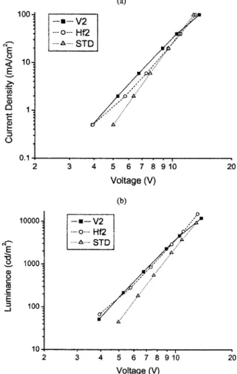
FIG. 6. J-V and L-V of V2-, Hf2-doped and standard devices.
FIG. 7. L-J and current efficiency-J of V2-, Hf2-doped and standard devices.
114515-4 Chen et al. J. Appl. Phys. 99, 114515共2006兲
the device performance and it is much more important than the energy barrier for the hole injection. The device with the Hf1-doped ITO layer has the lowest resistivity 共2 ohm cm兲 among three devices, its L-V curve also shows the difference, as shown in Fig. 4共b兲. In Fig. 5共a兲, the device with the Hf1-doped ITO layer has a relatively higher luminance in the L-J curves. From the current efficiency-J curves, as shown in Fig. 5共b兲, it’s also clear that the device with the Hf1-doped ITO layer has a higher current efficiency. The good perfor-mance of the device with the Hf1-doped ITO layer may be attributed to its low doping concentration and resistivity. Al-though they have a similar energy barrier共work function兲 for hole injection, the device with the Hf1-doped ITO layer has the highest carrier concentration, which may enhance the L and the current efficiency.
B. Devices with 5.2 eV work functions and various resistivities
These devices have similar work functions 共⬃5.2 eV兲 but significant differences in resistivity. The dif-ferent characteristics are clearly shown in both J-V and L-V curves in Fig. 6. In Fig. 6共a兲, the Hf2 curve is nonlinear, which is quite different from the other two. The large slope of the standard device can be understood by its high resistiv-ity. The large differences on their carrier concentrations lead
to completely different characteristics in both L-J and the current efficiency-J curves, as shown in Fig. 7. The device with the Hf2-doped ITO layer has the best performances among them. It shows that the high carrier concentration is much more important than the energy barrier for the hole injection in these devices.
C. Devices with 5.4 eV work functions and relatively large resistivities
These devices have similar large work functions 共⬃5.4 eV兲 and relatively large resistivities 共⬎2 K ohm cm兲. The linearity with almost the same slope in the J-V and L -V curves is shown in Fig. 8. Since they all have large resis-tivities, their carrier concentrations must be low. The L-J and the current efficiency-J curves were similar for devices with V3- and Zr3-doped ITO layer, but not for the device with H3-doped ITO layer, as shown in Fig. 9. The device with the Hf3-doped ITO has the highest luminance and current effi-ciency, although it has a similar work function and resistiv-ity. The exact reason is unclear, but it may be attributed to the dielectric property of the hafnium oxide in the Hf-doped ITO layer since all devices with the Hf-doped ITO layer have better performances than the others.
FIG. 8. J-V and L-V of V3-, Zr2- and Hf3-doped devices.
FIG. 9. L-J and current efficiency-J of V3-, Zr2- and Hf3-doped devices.
IV. CONCLUSION
We have compared the performance of OLEDs with dif-ferent metal-doped ITO buffer layers. The resistivities and the work functions of the metal-doped ITO layer were de-pendent on the concentrations of the doped metals. While the metal-doped ITO layers have lower work functions and re-sistivities, the devices usually have lower turn-on and oper-ating voltages as well. The device with the V1共6%V兲-doped ITO layer 共work function 5 eV, resistivity 10 ohm cm兲 has achieved a turn-on voltage below 3 V, an operating voltage below 7 V共at 10 mA/cm2兲, and a luminance of 1000 cd/m2
below 7 V. Though the metal-doped ITO layers have the same work function, the devices may have similar character-istics on the J-V curves, yet different on the L-J curves or the current efficiency-J curves. The devices with the Hf2 共4%Hf兲-doped ITO buffer layers show the highest luminance and current efficiency among all. At 100 mA/ cm2, a
lumi-nance of 15,000 cd/ m2, and a current efficiency of 15 cd/ A
have been achieved. The balance between the carrier concen-tration and the energy barrier for the hole injection is possi-bly responsible for such performance.
1C. W. Tang and S. A. VanSlyke, Appl. Phys. Lett. 51, 913共1987兲. 2C. Adachi, T. Tsutsui, and S. Saito, Appl. Phys. Lett. 55, 1489共1989兲. 3C. W. Tang, S. A. VanSlyke, and C. H. Chen, J. Appl. Phys. 85, 3610
共1989兲.
4R. H. Friend, R. W. Gymer, A. B. Holmes, J. H. Burroughes, R. N. Marks,
C. Taliani, D. D. C. Bradley, D. A. Dos Santos, J. L. Bredas, M. Logdlund, and W. R. Salaneck, Nature 397, 121共1999兲.
5J. Shi and C. W. Tang, Appl. Phys. Lett. 70, 1665共1997兲.
6C. Ganzorig, K.-J. Kwak, K. Yagi, and M. Fujihira, Appl. Phys. Lett. 79,
272共2001兲.
7H. Y. Yu, X. D. Feng, D. Grozea, Z. H. Lu, R. N. Sodhi, A.-M. Hor, and
H. Aziz, Appl. Phys. Lett. 78, 2595共2001兲.
8W. Hu and M. Matsumura, Appl. Phys. Lett. 81, 806共2002兲.
9W. H. Kim, A. J. Makinen, N. Nikolov, R. Shashidhar, H. Kim, and Z. H.
Kafafi, Appl. Phys. Lett. 80, 3844共2002兲.
10B. Low, F. Zhu, K. Zhang, and S. Chua, Appl. Phys. Lett. 80, 4659
共2002兲.
11S. A. VanSlyke, C. H. Chen, and C. W. Tang, Appl. Phys. Lett. 69, 2160
共1996兲.
12S. C. Kim, G. B. Lee, M.-W. Choi, Y. Roh, C. N. Wang, K. Jeong, J.-G.
Lee, and S. Kim, Appl. Phys. Lett. 78, 1445共2001兲.
13E. W. Forsythe, M. A. Abkowitz, Y. Gao, and C. W. Tang, J. Vac. Sci.
Technol. A 18, 1869共2000兲.
14S. M. Tadayyon, H. M. Grandin, K. Griffiths, P. R. Norton, H. Aziz, and Z.
D. Popovic, Org. Electron. 5, 157共2004兲.
15C. O. Poon, F. L. Wong, S. W. Tong, R. Q. Zhang, C. S. Lee, and S. T.
Lee, Appl. Phys. Lett. 83, 1038共2003兲.
16S. Y. Kim, J.-L. Lee, K.-B. Kim, and Y.-H. Tak, Appl. Phys. Lett. 86,
133504共2005兲.
17S. T. Lee, Z. Q. Gao, and M. R. Willis, Appl. Phys. Lett. 75, 1404共1999兲. 18Y. Shen, D. B. Jacobs, G. G. Malliaras, G. Koley, M. G. Spencer, and A.
Ioannodis, Adv. Mater.共Weinheim, Ger.兲 13, 1234 共2001兲.
19C. Qiu, H. Chen, Z. Xie, M. Wong, and H. S. Kwok, Appl. Phys. Lett. 80,
3485共2002兲.
20C.-M. Hsu and W.-T. Wu, Appl. Phys. Lett. 85, 840共2004兲.
21K. H. Ho, J.-S. Kim, J. H. Burroughes, H. Becker, S. F. Y. Li, T. M.
Brown, F. Cacialli, and R. H. Friend, Nature共London兲 404, 481 共2000兲.
22T. H. Chen, Y. Liou, T. J. Wu, and J. Y. Chen, Appl. Phys. Lett. 85, 2092
共2004兲.
23T. H. Chen, Y. Liou, T. J. Wu, and J. Y. Chen, Appl. Phys. Lett. 87,
243510共2005兲.
24H. Kim, J. S. Horwitz, W. H. Kim, S. B. Qadri, and Z. H. Kafari, Appl.
Phys. Lett. 83, 3809共2003兲.
25C. Chen and C. W. Tang, Appl. Phys. Lett. 79, 3711共2001兲.
114515-6 Chen et al. J. Appl. Phys. 99, 114515共2006兲