Enhanced ferroelectric properties of Pb ( Zr 0.53 Ti 0.47 ) O 3 thin films on SrRuO 3 /
Ru/SiO 2 / Si substrates
Y. K. Wang, T. Y. Tseng, and Pang Lin
Citation: Applied Physics Letters 80, 3790 (2002); doi: 10.1063/1.1480099 View online: http://dx.doi.org/10.1063/1.1480099
View Table of Contents: http://scitation.aip.org/content/aip/journal/apl/80/20?ver=pdfcov Published by the AIP Publishing
Articles you may be interested in
Huge Anisotropic Magnetoresistance In Epitaxial Sm 0.53 Sr 0.47 MnO 3 Thin Films AIP Conf. Proc. 1349, 703 (2011); 10.1063/1.3606052
Ferroelectric phase transition in Pb 0.92 Gd 0.08 ( Zr 0.53 Ti 0.47 ) 0.98 O 3 nanoceramic synthesized by high-energy ball milling
J. Appl. Phys. 94, 6091 (2003); 10.1063/1.1618915
Ferroelectric BaPbO 3 / PbZr 0.53 Ti 0.47 / BaPbO 3 heterostructures Appl. Phys. Lett. 81, 3624 (2002); 10.1063/1.1520332
Lattice strain and lattice expansion of the SrRuO 3 layers in SrRuO 3 / PbZr 0.52 Ti 0.48 O 3 / SrRuO 3 multilayer thin films
J. Appl. Phys. 92, 101 (2002); 10.1063/1.1483369
Asymmetry in the hysteresis loop of Pb(Zr 0.53 Ti 0.47 ) O 3 /SiO 2 /Si structures J. Appl. Phys. 86, 4467 (1999); 10.1063/1.371388
This article is copyrighted as indicated in the article. Reuse of AIP content is subject to the terms at: http://scitation.aip.org/termsconditions. Downloaded to IP: 140.113.38.11 On: Thu, 01 May 2014 06:19:38
Enhanced ferroelectric properties of Pb
„
Zr
0.53Ti
0.47…
O
3thin films
on SrRuO
3Õ
Ru
Õ
SiO
2Õ
Si substrates
Y. K. Wang and T. Y. Tsenga)
Department of Electronics Engineering and Institute of Electronics, National Chiao Tung University, Hsinchu 30050, Taiwan, Republic of China
Pang Lin
Institute of Materials Science and Engineering, National Chiao Tung University, Hsinchu 30049, Taiwan, Republic of China
共Received 12 November 2001; accepted for publication 19 March 2002兲
Highly 共110兲-oriented Pb(Zr0.53Ti0.47)O3 共PZT兲 films were deposited on SrRuO3 (SRO)/Ru/ SiO2/Si substrates using a sol–gel method, in which SrRuO3 films were deposited at various substrate temperatures. The crystallinity of the PZT films was improved after the annealing process. The leakage current, dielectric constant, and polarization versus electric-field characteristics of PZT films were strongly dependent on the annealing and deposition temperatures of the SRO films. The 650 °C annealed PZT film grown on SRO has a leakage current of 9⫻10⫺7A/cm2 at an applied field of 500 kV/cm, dielectric constant of 1306, remanent polarization ( Pr) of 40.1C/cm2 and coercive field (Ec) of 78.5 kV/cm at an applied voltage of 5 V. The PZT films indicated fatigue-free characteristics up to ⬃1.0⫻1012 switching cycles under 5 V bipolar pulse. © 2002 American
Institute of Physics. 关DOI: 10.1063/1.1480099兴
Ferroelectric thin films of Pb(ZrxTi1⫺x)O3 共PZT兲 have attracted attention for their applications on ferroelectric ran-dom access memory. However, previous reports have indi-cated that the use of a metal electrode with PZT thin films has serious fatigue problems at a relatively short number of switching cycles because of interface defects such as oxygen vacancies existing between PZT and the metal electrode.1 Conductive metallic oxide electrodes such as RuO2,
2 IrO2,
3 (La0.5Sr0.5) CoO3,4 BaRuO3,5 and SrRuO3 共Ref. 6兲 共SRO兲 were found to be effective in improving the fatigue proper-ties of PZT film capacitors. Oxide electrodes can act as sinks for oxygen vacancies to suppress polarization fatigue for long switching cycles. On the other hand, the selection of electrode material will determine the microstructure and properties of ferroelectric thin films. The formation of lattice- and chemistry-matched heterostructures of PZT films can be expected with perovskite oxide electrodes because of their similarity in lattice parameter and chemical behavior. This heterostructure usually enhances the ferroelectric char-acteristics of PZT films.7However, it is very difficult to de-posit preferentially oriented PZT and SRO films on silicon substrates, and most studies of epitaxial PZT films on SRO were deposited on SrTiO3 substrates.8 –10
In this study, we report on the preparation and properties of highly共110兲 oriented Pb(Zr0.53Ti0.47)O3thin films on con-ducting, highly 共110兲-preferentially oriented SRO bottom electrodes on silicon substrates.
SRO thin films were deposited on Ru/SiO2(100 nm)/Si(100) substrates at various temperatures by radio-frequency 共rf兲 magnetron sputtering, using a target made of packed SrRuO3 powders. The PZT films with a thickness of 200 nm were grown by a sol–gel method, and
annealing was performed in a tube furnace at various tem-peratures under O2atmosphere. The SRO top electrodes with an area of 4.9⫻10⫺5 cm2 were sputter deposited onto the PZT films at room temperature, and then thermally treated at 400 °C for 10 min to reduce interface defects during sputter-ing. The crystalline properties of the films were examined by x-ray diffraction共XRD, Siemens D5000兲 with Cu K␣ radia-tion. The surface morphology and microstructure were ob-served by using atomic-force microscopy共AFM, Digital In-struments Nanoscope III兲 and scanning electron microscopy
共SEM, Hitachi S-4700兲. The capacitance–voltage (C – V)
a兲Electronic mail: [email protected] FIG. 1. XRD patterns of SRO films deposited on Ru/SiOvarious temperatures indicated. 2/Si substrates at
APPLIED PHYSICS LETTERS VOLUME 80, NUMBER 20 20 MAY 2002
3790
0003-6951/2002/80(20)/3790/3/$19.00 © 2002 American Institute of Physics
This article is copyrighted as indicated in the article. Reuse of AIP content is subject to the terms at: http://scitation.aip.org/termsconditions. Downloaded to IP: 140.113.38.11 On: Thu, 01 May 2014 06:19:38
characteristics were measured with an impedance-gain phase analyzer 关Hewlett-Packard 共HP兲 4194A兴 at 100 kHz. The current–voltage (I – V) measurements were performed by us-ing a semiconductor parameter analyzer 共HP4156B兲. The ferroelectric properties of the films were measured at 100 kHz using a RT66A ferroelectric tester 共Radiant Technolo-gies, Inc.兲.
Figure 1 shows the XRD patterns of SRO films on Ru/SiO2/Si substrates deposited at various temperatures. The deposited SRO films exhibit a highly 共110兲-preferred orientation on the Ru共002兲 films even if the deposition tem-perature is as low as at 300 °C. The increase in SRO共110兲 peak intensity with an increase of temperature implies an improved crystallinity occurred in the films deposited at higher temperature. We found that the RuO2(110) peak ap-peared in 450 °C deposited film owing to oxidation reaction at the interface during deposition, and an additional Ru共100兲 peak also appeared in the meantime. The XRD patterns of PZT films deposited on 450 °C-grown SRO/Ru/SiO2/Si sub-strates and annealed at various temperatures are shown in Fig. 2. A strong 共110兲-preferred orientation appears in the PZT films annealed at 450 °C, and this preferred orientation is enhanced with increasing annealing temperature up to 700 °C. We found in x-ray analysis共not shown here兲 that the PZT共100兲 peak also appeared when 300– 400 °C-grown SRO electrodes were used. The PZT films deposited at 300 °C on SRO showed an enhanced共100兲 peak as the annealing tem-perature increased; however, PZT films deposited at 350 and
400 °C showed no change in the 共100兲 peak intensity as a function of temperature.
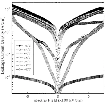
The dielectric constant and loss tangent of the PZT films annealed at various temperatures are listed in Table I. The dielectric constant and loss tangent increase with an increase in temperature, which have the highest values of 1541 and 0.137, respectively, for 700 °C-annealed films. Such a high dielectric constant may be attributed to better crystallinity, grain size, and the presence of a thin strain layer between PZT and SRO leading to increased polarization in highly oriented 700 °C-annealed films. Figure 3 shows the leakage current density of PZT films deposited on 450 °C-grown SRO/Ru/SiO2/Si substrates. The symmetry of the curves in-dicates the same barrier height for both top and bottom elec-trodes. The leakage current density for 400 °C-annealed PZT has a small value of less than 10⫺9A/cm2 because of the poor crystallization, whereas the 650 °C-annealed PZT has a leakage current of 9⫻10⫺7A/cm2 at an applied field of 500 kV/cm. It shows that the leakage current increases at high annealing temperature, which is consistent with the result of the loss tangent. This increase may be attributed to the grain growth at high temperature, supplying short-circuit paths when the bias is applied. The grain growth accompanied with the annealing temperature is confirmed by using AFM and SEM observations, as shown in Figs. 4共a兲–4共c兲 and 4共d兲– 4共f兲, respectively. It indicates that the film annealed at higher temperature has a larger grain size. In addition, the defect induced by high-temperature annealing, such as lead loss, may also lead to higher leakage current and loss tangent. The FIG. 2. XRD patterns of PZT films deposited on 450 °C-grown
SRO/Ru/SiO2/Si substrates annealed at various temperatures indicated.
FIG. 3. I – V characteristics of PZT thin films deposited on 450 °C-grown SRO/Ru/SiO2/Si substrates and afterward annealed at various temperatures
indicated.
TABLE I. Dielectric constant and loss tangent of PZT thin films deposited on 450 °C-grown SRO and annealed at various temperatures.
Annealing temperature (°C) 400 450 500 550 600 650 700 Dielectric constant 33 165 641 940 1071 1306 1541
Loss tangent 0.011 0.014 0.049 0.105 0.110 0.114 0.137
3791 Appl. Phys. Lett., Vol. 80, No. 20, 20 May 2002 Wang, Tseng, and Lin
This article is copyrighted as indicated in the article. Reuse of AIP content is subject to the terms at: http://scitation.aip.org/termsconditions. Downloaded to IP: 140.113.38.11 On: Thu, 01 May 2014 06:19:38
PZT films annealed above 700 °C have a very high leakage current and low breakdown strength. On the basis of AFM and SEM plane-view observations, as indicated in Figs. 4共c兲 and 4共f兲, a high surface roughness with protruding grains can be found in 750 °C-annealed PZT film. After applying bias to the top electrode, the high surface roughness of the film could induce the local field that caused the PZT breakdown at low electric field.
The characteristics of fatigue of the 650 °C-annealed PZT films are depicted in Fig. 5, indicating that highly 共110兲-oriented PZT films deposited on SRO/Ru/SiO2/Si substrates do not show any deterioration after⬃1012switching cycles. The polarization–electric-field hysteresis loops of 650 °C-annealed PZT deposited on SRO prepared at various substrate temperatures is also indicated in the inset to Fig. 5. The PZT film deposited on the 350 °C-grown SRO electrode has a higher remanent polarization ( Pr) value of 36.6C/cm2, but the Pr value is only 26.6C/cm2 for that deposited on 300 °C-grown SRO. The Pr value of PZT on 300 °C-grown SRO is smaller because this PZT film has a polycrystalline structure; however, highly 共110兲-preferentially oriented PZT films can be obtained when the bottom electrode SRO was deposited above 350 °C.
In conclusion, we have demonstrated共110兲 preferentially oriented SRO bottom electrodes deposited on Ru/SiO2/Si substrates by rf sputtering. PZT thin films deposited on those bottom electrodes also have highly 共110兲-preferred orienta-tion. The leakage current of PZT films annealed at lower temperatures is smaller than those annealed at higher tem-peratures, and the reasons for this phenomenon are the grain growth, lead-loss-induced defect, and local field. The
dielec-tric constant and remanent polarization also increased with an increase of the annealing temperature. PZT films are fa-tigue free after⬃1012switching cycles.
This work was supported by the National Science Coun-cil R.O.C. under Contract No. NSC 89-2215-E-009-027.
1P. K. Larsen, G. J. M. Dormans, D. J. Taylor, and P. J. van Veldhoven, J. Appl. Phys. 76, 2405共1994兲.
2S. D. Bernstein, T. Y. Wong, Y. Kisler, and R. W. Tustison, J. Mater. Res.
8, 12共1993兲.
3
T. Nakamura, Y. Nakao, A. Kamisawa, and H. Takasu, Jpn. J. Appl. Phys., Part 1 33, 5207共1994兲.
4R. Ramesh, T. Sands, and V. G. Keramidas, J. Electron. Mater. 23, 19 共1994兲.
5
C. M. Chu and P. Lin, Appl. Phys. Lett. 70, 249共1997兲.
6C. B. Eom, R. B. VanDover, J. M. Phillips, D. J. Werder, J. H. Marshall, C. H. Chen, R. J. Cava, and R. M. Fleming, Appl. Phys. Lett. 63, 2570
共1993兲. 7
K. P. Jayadevan and T. Y. Tseng, Proceedings of ICCE/8, 5–11 August 2001, Tenerife, Spain共2001兲, p. 397.
8J. H. Kim, A. T. Chien, F. F. Lange, and L. Wills, J. Mater. Res. 14, 1190 共1999兲.
9C. M. Foster, G. R. Bai, R. Csencsits, J. Vetrone, R. Jammy, L. A. Wills, E. Carr, and Jun Amano, J. Appl. Phys. 81, 2349共1997兲.
10K. Nagashima, M. Aratani, and H. Funahubo, J. Appl. Phys. 89, 4517 共2001兲.
FIG. 4. AFM and SEM images of PZT thin films annealed at various tem-peratures indicated.
FIG. 5. Fatigue behavior of 650 °C-annealed PZT films deposited on 450 °C-grown SRO/Ru/SiO2/Si, with a 100 kHz bipolar square-wave
peak-to-peak fatigue voltage of 10 V. The inset shows polalization–electric-field hysteresis loops of 650 °C-annealed PZT thin films deposited on SRO bot-tom electrodes prepared at various temperatures indicated.
3792 Appl. Phys. Lett., Vol. 80, No. 20, 20 May 2002 Wang, Tseng, and Lin
This article is copyrighted as indicated in the article. Reuse of AIP content is subject to the terms at: http://scitation.aip.org/termsconditions. Downloaded to IP: 140.113.38.11 On: Thu, 01 May 2014 06:19:38