2.4
High Quality La203 and
A1203
Gate Dielectrics with Equivalent Oxide Thickness 5-10A
Albert Chin, Y. H. Wu,
S.
B. Chen, C. C. Liao, and
W. J.
Chen'
Dept. of Electronics Eng., National Chiao Tung Univ., Hsinchu, Taiwan 'Dept. of Mechanical Materials Eng., National Yun-Lin Polytechnic Inst., Huwei, TaiwanTel: +886-3-573 184 I , Fax: +886-3-5724361, E-mail: [email protected] Abstract
High quality La,O, and AI,O, are fabricated with EOT of 4.8 and 9.6A, leakage current of 0.06 and 0.4A/cm and D,, of both 3x10'" eV-'/cm2, respectively. The high K is further evidenced from high MOSFET 's I, and g, with low I,, Good SILC and QeD are obtained and comparable with SiO,. The low EOT is due to the high thermodynamic stability in contact with Si and stable after H
,
annealing up to 550°C.Introduction
Although high K gate dielectrics have attracted much attention recently, further reduction of EOT may be limited by the interface reaction region between high K material and Si [I], [2]. Therefore, the search for thermodynamically stable high K dielectric directly on Si is important to meet future sub-I 0A requirement. Besides the required good electrical properties such as low interface trap density (D ,,), low leakage current, high breakdown field (E BD) and good reliability, high K material must also be compatible with existing VLSI process. Thus, good stability with H
,
and high transition temperature from amorphous to crystal [2] are necessary to prevent dielectric degradation by H,
and crystalline structure created defects or dislocations during strain relaxation in process. Previously, we have reported that amorphous AI ,O,directly on Si can meet near all the requirements and stable up to 1000°C [3], except that EOT (2 1
A)
and D ,I ( 1 x I O " eV-'/cm') are still high. The high D is unacceptable for IC because of the increased noise [4]. In this paper, we have used amorphous La,O, (K-27) to achieve 4.8A EOT and reduced AI 2Q3 EOT to 9.6& where La,O, has similar property as AI ,O, but witheven better thermal stability on Si (Table I ) . I n addition to respective low leakage current of 0.06 and 0.4A/cm for La,O, and Al,O,, both dielectrics now have good D I, (3x10'" eV-
'/cm2), E,,, SILC, and QBD as compared with SiO,. Experimental
To avoid any K value reduction, interfacial native oxide is suppressed by HF-vapor passivation and in-sifu desorption [3] followed by an immediate La or AI evaporation. Because La or AI is highly reactive with 0
,,
low oxidation temperatures 1400°C is used to reduce metal diffusion into Si. The formed oxides were further annealed in N at 900°C. To reduce gate depletion, AI gate is used for MOS capacitor and transistor to evaluate the electrical characteristics. H annealing at 450- 550°C is performed to study the stability with H,. Besides achieved higher K, suppression of native oxide is important to obtain a smooth interface, low D ,,, and high reliability in our previously achieved atomically smooth ultra-thin oxides.Results and Discussion
A. Cafe cupmifor:
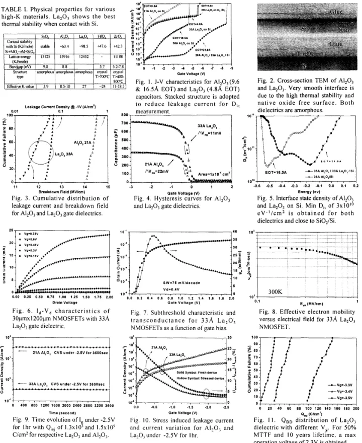
Fig. I presents the J-V characteristics of La ,O, and A120, capacitors. Comparable leakage current for La 20, on Si or
16
0-7803-6305-4/00/$10.00 0 2000 IEEESi, ,Ge,, is obtained that is important for high mobility PMOS [5]. The stacked AI,O,/La,O, is used to reduce leakage current for C-V to obtain D In order to get accurate K and EOT , the oxide thickness is carefully examined by both ellipsometer and TEM in Fig. 2. The very uniform oxide and smooth interface are due to native oxide free surface and high thermal stability in Table I as contact with Si. Therefore, low EOT can be expected. Fig. 3 shows the cumulative values for high K oxides, and leakage current of O.O6A/cm for La,O, and 0.4 A/cm2 for AI,O, are obtained. Fig. 4 is the C-V curves and K values of 27 and 8.5 are measured for respective La ,O, and AI,O, that gives the low 4.8A and 9.6A EOT (without QM correction). Small hysterisis of 11 and 22mV are measured for respective dielectrics that indicates good quality because of applied high annealing temperature without transition to crystal structure [2]. Fig. 5 shows the measured D
,,
of 3x10'" eV-'/cm2 from both capacitors. This low DI,
close to thermal SiO, is extremelyimportant for circuit to lower I/f noise [4].B Punsiiforpevormance with 4
8d
EOTWe have further fabricated wide gate MOSFETs with 4.8A EOT. Figs. 6 shows the device 1 d-Vd, and important ld-Vg and g,,, are plotted in Fig. 7. The very high current drive and g, are due to high K that gives a K of -27 consistent with C-V measurement. Good device pinch-off lor< 1 O-'"A/pm and small sub-threshold swing of 75mV/decade are observed, and the small swing also suggests the low D II. The effective mobility
is further plotted in Fig. 8. The electron mobility is comparable with published universal mobility data for thermal
SiO, because of low D,,.
C Reliubiky:
Fig. 9 shows the gate dielectrics under a -2.5V constant stress for 1 hr with total QUI,, of 1 . 3 ~ 1 O 3 and 1 . 2 ~ 105C/cm2 for La,O, and AI,O,, respectively. No significant charge trapping is occurred during stress, and small SILC for both dielectrics is observed in Fig. IO. Good reliability for 4.8 8, EOT La,O, is evidenced from the high Q o D i n Fig. 11 and comparable with current SiO, [6]. The good SILC and Q B D may be due to the high lattice energy in Table 1. From the 50% failure time, an extrapolated max voltage of 2.3V is obtained for I O years lifetime that suggests good reliability for VLSI application with 4.8A EOT and small leakage of 0.06A/cm2 atlV.
Conclusions
We have shown that La,O, is good for EOT down to 5A and AI,O, is highly competitive for EOT 2lOA.
References
I . B. H . Lee e7
UL
/EDM Ech. 022. ( 1 999). p. 133. 2. Y. Mae/(l/,fEDMEeh. Or% (1999),p.149. 3. A. Chin e/uL@?y, on VLSfEch.(1999),p.135. 4. H. Kiniijinia c/u( $ h g ~ . on YLS/Tech.(1999), p.119. 5. Y. H. Wu and A. Chin, ZEEEEDL March, (2000).6. Y. Taur & T. H. Ning, Fund. Modem VLSI Devices, p. 106 ( 1 998).
.
0.00 0.25 0.50 0.75 1.00 1.25 1.50 1.75 2.00
Drain Voltage
Fig. 6 . l d - V d c h a r a c t e r i s t i c s o f 30pmx1200pm NMOSFETs with 33A La,O, gate dielectric.
--e 38A AI,O, I 3 3 A La,O, I SI
-38A AI,O,IS* E O T - 1 6 5 A d 10': -
<:
:;
- S W z 7 5 m v l d e c a d e V d = O . I V a U 4 0 35 3 0 20; 15-& 10 5 0 10.'1
-1
0 400 800 1200 1600 2000 2400 2800 3200 3600 T i m e ( s e c o n d )Fig. 9. Time evolution of I, under - 2 . W for I h r with Q,,,, of 1 . 3 ~ 1 0 ~ and 1 . 5 ~ 1 0 ~
C/cm2 for respective La,O, and A1203.
0.0 0 . 2 0 . 4 0.5 0.8 1.0 1.2 1.4 1.6 1.8 2.0 G a t e Voltage ( V )
Fig. 7. Subthreshold characteristic and t r a n s c o n d u c t a n c e f o r 3 3 A La,O, NMOSFETs as a function ofgate bias.
10' I , 3 0
10.4 . , . , , , . , . I o
-
0.0 4 . 5 -1.0 -1.5 -2.0 -2.5Gate Voltage (V)
Fig. IO. Stress induced leakage current and current variation for A120, and
La203 under -2.W for I hr.
10' 0 U
,g
5
-E1
1
'']
300K , , , , , , , ,1
10' E," (MVlcm) 0.1 1Fig. 8. Effective electron mobility versus electrical field for 33A La,O, NMOSFET. 100 ~ 90 -
L
8 0 - $ 70: 5 6 0 - - . U . $ 5 0 -2
3 0 : -vg=-3.3v 20: -vg=.3.4v - . 4 0 --
10- tvg--3.5v 0 , . , , , . , . , . , . , . , . , . ,Fig. 1 1 . Q e D distribution of La,O, dielectric with different V,. For 50% MTTF and I O years lifetime, a max operation voltage of 2.3V is obtained.
0 20 40 60 80 100 1 2 0 140 160 180 :
P,, (Clem')
0