Electrical characterization of organic light-emitting diodes using dipotassium
phthalate as n -type dopant
Meng-Huan Ho, Ming-Ta Hsieh, Teng-Ming Chen, Jenn-Fang Chen, Shiao-Wen Hwang, and Chin H. Chen
Citation: Applied Physics Letters 93, 083505 (2008); doi: 10.1063/1.2976139
View online: http://dx.doi.org/10.1063/1.2976139
View Table of Contents: http://scitation.aip.org/content/aip/journal/apl/93/8?ver=pdfcov Published by the AIP Publishing
Articles you may be interested in
Electronic structures of Ba-on- Alq 3 interfaces and device characteristics of organic light-emitting diodes based on these interfaces
J. Appl. Phys. 105, 083705 (2009); 10.1063/1.3106604
Very low voltage and stable p - i - n organic light-emitting diodes using a linear S,S-dioxide oligothiophene as emitting layer
Appl. Phys. Lett. 94, 063510 (2009); 10.1063/1.3072798
Incorporation of cobaltocene as an n -dopant in organic molecular films J. Appl. Phys. 102, 014906 (2007); 10.1063/1.2752145
Highly power efficient organic light-emitting diodes with a p -doping layer Appl. Phys. Lett. 89, 253504 (2006); 10.1063/1.2405856
Enhancement of hole injection using O 2 plasma-treated Ag anode for top-emitting organic light-emitting diodes
Appl. Phys. Lett. 86, 012104 (2005); 10.1063/1.1846149
This article is copyrighted as indicated in the article. Reuse of AIP content is subject to the terms at: http://scitation.aip.org/termsconditions. Downloaded to IP: 140.113.38.11 On: Wed, 30 Apr 2014 22:56:33
Electrical characterization of organic light-emitting diodes using
dipotassium phthalate as n-type dopant
Meng-Huan Ho,1,a兲 Ming-Ta Hsieh,2,a兲 Teng-Ming Chen,1 Jenn-Fang Chen,2 Shiao-Wen Hwang,3and Chin H. Chen3
1
Department of Applied Chemistry, National Chiao Tung University, Hsinchu, Taiwan 300, Republic of China
2
Department of Electrophysics, National Chiao Tung University, Hsinchu, Taiwan 300, Republic of China 3
Display Institute, Microelectronics and Information Systems Research Center, National Chiao Tung University, Hsinchu, Taiwan 300, Republic of China
共Received 13 May 2008; accepted 31 July 2008; published online 26 August 2008兲
An efficient n-doped electron transport layer composed of 4,7-diphenyl-1,10-phenanthroline 共BPhen兲 and dipotassium phthalate 共PAK2兲 has been developed. By temperature-dependent admittance spectroscopy, the incorporation of PAK2 into BPhen is found to raise the Fermi level from 1.7 eV to only around 0.5 eV below BPhen’s lowest unoccupied molecular orbital, which further enhances the efficiency of electron injection from an Al cathode. When this n-doped layer is adopted in an organic light-emitting diode device, the green fluorescent 10-共2-benzothiazolyl兲-1,1,7,7-tetramethyl-2,3,6,7-tetrahydro-1H , 5H , 11H-benzo关l兴-pyrano关6,7,8-ij兴quinolizin-11-one do-ped device can achieve a current efficiency of 16 cd/A and a power efficiency of 10.9 lm/W at 1000 cd/m2. © 2008 American Institute of Physics.关DOI:10.1063/1.2976139兴
Since efficient organic light-emitting diodes 共OLEDs兲 were discovered, developing OLEDs for display applications has attracted much attention.1,2 Reducing the power con-sumption of OLEDs requires increasing the carrier injection from the electrode to the transporting layer. The commonly used strategy for electron injection into an electron transport layer 共ETL兲 is to insert a thin lithium fluoride 共LiF兲 inter-layer between an Al cathode and a tris共8-hydroxyquinoline兲aluminum 共Alq3兲 layer.3 The mechanism
of electron injection into the LiF/Al composite cathode is a chemical reaction between Al and LiF.4 Another class of electron injection materials is organometallic complexes with reactive metals such as lithium carboxylates5 and 2-共hydroxyl兲quinoline lithium 共Liq兲.6
However, the effective-ness of these electron injection materials is very sensitive to the choice of metal, and only Al has been found to provide good device performance.
An alternative approach for an efficient carrier injection is to introduce a p-i-n structure into an OLED device, en-abling the operating voltage to be considerably reduced in both fluorescent7and phosphorescent8 systems. Highly con-ductive n-doped layers have been shown to enhance the in-jection of electrons from the contacts and to reduce the Ohmic losses in these layers. The most widely investigated
n-type dopants for the ETL are alkali metals, such as cesium9
and lithium.10 However, they suffer from the necessity of a high doping ratio often of the order of 50% to achieve high conductivity, which often alters the host matrix properties. These methods require special equipments and care in han-dling reactive metals; they are thus not convenient for fabri-cation. In 2004, Canon Inc. reported that cesium carbonate 共Cs2CO3兲,11 either vacuum deposited as an individual layer
over the organic electron transport material or codeposited with the organic electron transport material, facilitates
elec-tron injection from a wide range of metal electrodes. How-ever, fabrication can be performed only at a high deposition temperature of Cs2CO3 共around 500 °C under a vacuum兲.
Therefore, finding a satisfactory n-type dopant with a low deposition temperature is important in developing OLEDs with low power consumption.
This letter develops an n-doped ETL that consists of dipotassium phthalate 共PAK2兲 incorporated into 4,7-diphenyl-1,10-phenanthroline 共BPhen兲 and the electrical characteristics by measuring current-voltage共I-V兲 and using temperature-dependent admittance spectroscopy共AS兲. PAK2 can grow at a stable rate at around 330 ° C at a base vacuum of 10−7torr, significantly facilitating the fabrication process. A series of electron-only devices was also fabricated to study the electron injection and electrical characteristics. The electron-only device structure was indium tin oxide 共ITO兲/Alq3共60 nm兲/n-doped ETL 共30 nm兲/Al 共150 nm兲. In
devices A, B, C, and D, the doping concentrations of PAK2 in BPhen as n-doped ETL were 0%, 5%, 10%, and 20%, respectively. To demonstrate that PAK2 is more effective than the conventional LiF/Al composite cathode, the follow-ing 10-共2-benzothiazolyl兲-1,1,7,7-tetramethyl-2,3,6,7-tetrahydro-1H , 5H , 11H-benzo关l兴pyrano-关6,7,8-ij兴quinolizin-11-one 共C-545T兲 green-doped OLED devices, whose struc-ture was ITO/CFx/NPB 共60 nm兲/Alq3: 1% C545T
共37.5 nm兲/Alq3 共37.5 nm兲/electron injection layer 共EIL兲/Al
共150 nm兲, was fabricated, while the EIL of devices I and II were LiF共1 nm兲 and BPhen: 5% PAK2 共5 nm兲, respectively. Figure 1 plots the I-V characteristics of electron-only devices and reveals that the PAK2-doped devices B, C, and D all greatly outperform the undoped device A, indicating that doping PAK2 into BPhen promotes the injection of elec-tron from the Al cathode. Device B with 5% PAK2 has better
I-V characteristics than devices C and D, even at a small
applied bias 共inset in Fig. 1兲, probably due to the different extents of electron injection with various PAK2 doping con-centrations. The electrical properties of this n-doped layer
a兲Authors to whom correspondence should be addressed. Electronic
ad-dresses: [email protected] and [email protected].
APPLIED PHYSICS LETTERS 93, 083505共2008兲
0003-6951/2008/93共8兲/083505/3/$23.00 93, 083505-1 © 2008 American Institute of Physics
This article is copyrighted as indicated in the article. Reuse of AIP content is subject to the terms at: http://scitation.aip.org/termsconditions. Downloaded to IP: 140.113.38.11 On: Wed, 30 Apr 2014 22:56:33
were investigated by temperature-dependent AS with an equivalent circuit model to elucidate this phenomenon. 共De-tails of the methods and theories can be found elsewhere.兲12–14 Figure 2共a兲 depicts the 300 K capacitance-frequency 共C-F兲 measured at 2 V and the conductance/ frequency-frequency 共G/F-F兲 spectra measured from 0 to 2 V on device B. The spectra show two capacitance drops and corresponding G/F peaks at the inflexion fre-quency. The G/F-F spectra show a bias-independent peak at a high-frequency region, suggesting the presence of series resistances. They also show a bias-dependent peak at a low-frequency region, which is associated with the resistance of the BPhen layer. This argument is inferred from the observa-tion that the C-F spectra and G/F-F spectra of devices C and D are similar to those of device B共not shown here兲. Device A shows only the bias-independent peak at the high-frequency region. In the C-F spectra, the capacitance 共4.7 nF兲 measured at 100 Hz corresponds to the thickness of the Alq3layer according to the parallel-capacitor model with
a dielectric constant of 3.5.15As the frequency increases, the capacitance drops to a plateau whose value 共3.2 nF兲 corre-sponds to a series combination of the Alq3and BPhen layers.
Hence, the RC time constant of the BPhen can then be de-termined from the inflexion frequency. As the frequency fur-ther increases, the capacitance drops to zero, which is due to
parasitic effects of lead/contact series resistances. The BPhen peak of the doped devices cannot be clearly detected at a bias of under 1 V because of a high energy barrier between Al and BPhen, limiting the AS measurements. The energy bar-rier becomes negligible as the bias is increased over 1 V, and therefore, the electrical properties of BPhen can be charac-terized. Moreover, the BPhen peak of the undoped device cannot be observed even at a high applied bias, suggesting that the energy barrier between the work function of Al 共4.2 eV兲 and the lowest unoccupied molecular orbital 共LUMO兲 of BPhen 共2.9 eV兲 in device A is too high to be measured by AS. Figure2共b兲displays temperature-dependent
G/F-F spectra at 1.4 V for device B 共the spectra at 1.2, 1.6,
1.8, and 2.0 V are similar to those at 1.4 V兲. The BPhen peak evidently depends significantly on temperature, and the series-resistance peaks are all independent of temperature. Furthermore, the frequency 共F兲 of the BPhen peak corre-sponds to the RC time constant of BPhen. Hence, the activa-tion energy 共Ea兲 of the BPhen layer is given by a simple
geometric equation,
F = F0exp
冉
− Ea KT
冊
,where F0 is the pre-exponential factor, E
a is the activation
energy, which represents the energy separation between the edge of the Fermi level and the LUMO band, K is Boltz-mann’s constant, and T is the temperature. The inset in Fig.3 plots ln共F兲 versus 1000/T, which yields the Eavalue of the
BPhen in device B at various biases. Figure3 plots the rela-tionship between Eaand the applied voltage of PAK2-doped
devices. The calculated Ea values of the PAK2-doped
de-vices are around 0.5– 0.6 eV, which is much smaller than the
Ea共half band-gap, 1.7 eV兲 of pure BPhen 共the Fermi level of
ideally pure organic semiconductors should be close to the middle of the gap兲.16 Based on the AS results, the incorpo-ration of PAK2 into BPhen increases the Fermi level of BPhen from deep to shallow, further reducing the interface energy barrier and increasing the efficiency of electron injec-tion from the Al cathode. Moreover, device B has the small-est Ea value, according to AS, whose result agrees
com-pletely with the I-V measurement. That increasing PAK2
FIG. 1. Current-voltage共I-V兲 characteristics of electron-only devices in the linear scale. Inset: logarithmic scale under a small bias.
FIG. 2. 共a兲 Capacitance-frequency 共C-F兲 spectrum of device B at 2 V and conductance/frequency-frequency 共G/F-F兲 spectra of device B from 0 to 2 V at room temperature;共b兲 temperature-dependent G/F-F spectra of device B at 1.4 V.
FIG. 3. Relationship between Eaand applied voltage of devices B, C, and
D. Inset: ln共F兲 vs 1000/T at various biases for device B.
083505-2 Ho et al. Appl. Phys. Lett. 93, 083505共2008兲
This article is copyrighted as indicated in the article. Reuse of AIP content is subject to the terms at: http://scitation.aip.org/termsconditions. Downloaded to IP: 140.113.38.11 On: Wed, 30 Apr 2014 22:56:33
incorporation from 5% to 20% does not further improve the performance of electron injection is attributable to fallows from the effect of carrier quenching and defect generations. Figure 4 plots the luminance-current density-voltage 共L-J-V兲 curves of devices I and II. Device II with n-doped ETL can achieve a higher current density and luminance at a lower voltage than device I with a conventional LiF/Al com-posite cathode. Device II achieved a power efficiency of 10.9 lm/W at 1000 cd/m2共16 cd/A at 4.6 V兲, which is 40%
higher than that of conventional device I at 1000 cd/m2
共7.8 lm/W and 12.7 cd/A at 5.0 V兲. These results clearly demonstrate that the n-doping effect of PAK2 in BPhen fur-ther enhanced the electron injection. The dominant carrier in most Alq3-based OLEDs is the injected hole.17The
improve-ment of the electron injection from the cathode not only reduces the drive voltage but also balances the carrier recom-bination in the device, which we believe is the main reason for the enhanced efficiency of the device. The inset in Fig.5
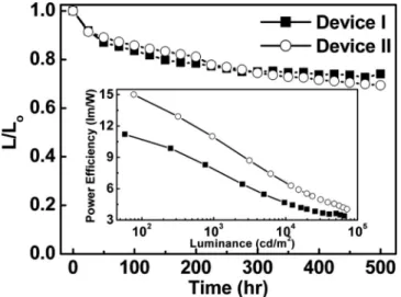
plots the power efficiency against luminance for devices I and II. The power efficiency of device II at 100 cd/m2 can be as high as 14.6 lm/W 共at 3.3 V兲, suggesting that the in-jection of electrons from the cathode of this PAK2-doped ETL is efficient even at a low drive voltage. The operational lifetimes of devices I and II under a constant current density of 20 mA/cm2were also measured in a dry box, as shown in
Fig.5. The t70共time for the luminance to decline to 70% of the initial luminance兲 values of both devices are approxi-mately 500 h. Based on the assumption of scalable Coulom-bic degradation,18the half-lives共t1/2兲 of devices I and II can
be projected to 28 900 and 36 200 h at 100 cd/m2,
respec-tively. The operational stability of device II with n-doped ETL is clearly comparable to that of conventional device I.
In summary, I-V measurement and temperature-dependent AS indicated that the incorporation of PAK2 into BPhen increases the Fermi-level to only around 0.5 eV be-low BPhen’s LUMO band, further enhancing the efficiency of electron injection from Al cathode. Additionally, the low deposition temperature of PAK2 substantially facilitates the fabrication processes. When this n-doped layer is incorpo-rated in the OLED device, the C545T-doped device achieves a current efficiency of 16 cd/A and a power efficiency of 10.9 lm/W at 1000 cd/m2.
This work was supported by the National Science Coun-cil of Taiwan共NSC 96-2218-E-009-009兲 and Chunghwa Pic-ture Tubes, Ltd. 共CPT兲 of Taoyuan, Taiwan.
1C. W. Tang and S. A. Vanslyke,Appl. Phys. Lett. 51, 913共1987兲. 2L. S. Hung and M. G. Mason,Appl. Phys. Lett. 78, 3732共2001兲. 3L. S. Hung, C. W. Tang, and M. G. Mason, Appl. Phys. Lett. 70, 152
共1997兲.
4P. He, S. D. Wang, S. T. Lee, and L. S. Hung,Appl. Phys. Lett. 82, 3218
共2003兲.
5C. Ganzorig and M. Fujihira,Jpn. J. Appl. Phys., Part 238, L1348共1999兲. 6S. H. Kim, J. Jang, and J. Y. Lee,Appl. Phys. Lett. 91, 103501共2007兲. 7J. Huang, M. Pfeiffer, A. Werner, J. Blochwitz, S. Liu, and K. Leo,Appl.
Phys. Lett. 80, 139共2002兲.
8G. F. He, O. Schneider, D. S. Qin, X. Zhou, M. Pfeiffer, and K. Leo,J.
Appl. Phys. 95, 5773共2004兲.
9J. H. Lee, M. H. Wu, C. C. Chao, H. L. Chen, and M. K. Leung,Chem.
Phys. Lett. 416, 234共2005兲.
10J. Kido and T. Matsumoto,Appl. Phys. Lett. 73, 2866共1998兲.
11T. Hasegawa, S. Miura, T. Moriyama, T. Kimura, I. Takaya, Y. Osato, and
H. Mizutani, Proceedings of the Society for Information Display, Seattle, Washington, 2004共unpublished兲, p. 28.
12M. T. Hsieh, C. C. Chang, J. F. Chen, and C. H. Chen,Appl. Phys. Lett.
89, 103510共2006兲.
13W. G. Oldham and S. S. Naik,Solid-State Electron. 15, 1085共1972兲. 14S. W. Tsang, S. K. So, and J. B. Wu,J. Appl. Phys. 99, 013706共2006兲. 15S. Odermatt, N. Ketter, and B. Witzigmann,Appl. Phys. Lett. 90, 221107
共2007兲.
16M. Pfeiffer, K. Leo, and N. Karl,J. Appl. Phys. 80, 6880共1996兲. 17H. Aziz, Z. D. Popovic, N.-X. Hu, A.-M. Hor, and G. Xu,Science 283,
1900共1999兲.
18S. A. Van Slyke, C. H. Chen, and C. W. Tang,Appl. Phys. Lett.69, 2160
共1996兲. FIG. 4. Luminance-current density-voltage共L-J-V兲 curves of devices I and
II.
FIG. 5. Operational stability of devices I and II. Inset: power efficiency versus luminance characteristics of devices I and II.
083505-3 Ho et al. Appl. Phys. Lett. 93, 083505共2008兲
This article is copyrighted as indicated in the article. Reuse of AIP content is subject to the terms at: http://scitation.aip.org/termsconditions. Downloaded to IP: 140.113.38.11 On: Wed, 30 Apr 2014 22:56:33