810 IEEE TRANSACTIONS ON ELECTROMAGNETIC COMPATIBILITY, VOL. 50, NO. 4, NOVEMBER 2008
Investigation on Robustness of CMOS Devices
Against Cable Discharge Event (CDE) Under
Different Layout Parameters in a
Deep-Submicrometer CMOS Technology
Ming-Dou Ker, Fellow, IEEE, and Tai-Hsiang Lai
Abstract—Cable discharge events (CDEs) have been found to be the major root cause of inducing hardware damage on Ethernet ICs of communication interfaces in real applications. Still, there is no device-level evaluation method to investigate the ro-bustness of complementary metal–oxide–semiconductor (CMOS) devices against a CDE for a layout optimization in silicon chips. The transmission-line pulsing (TLP) system was the most impor-tant method used to observe the electrical characteristics of semi-conductor devices under human-body model (HBM) electrostatic discharge (ESD) stress. To understand the physical characteris-tics and CDE robustness of on-chip protection devices, the long-pulse transmission-line pulsing (LP-TLP) system is proposed in this paper and used to simulate the influence of CDE on Ethernet-integrated circuits. The secondary breakdown characteristics of the CDE protection devices under different layout styles and pa-rameters can be measured and analyzed by the proposed LP-TLP with pulsewidths of 500 or 1000 ns. Furthermore, measured results using the LP-TLP system are compared with results measured by the traditional 100-ns TLP system. The experimental results with silicon devices in 0.18-µm CMOS process have shown that the CDE robustness of n-channel metal–oxide–semiconductor (NMOS) and p-channel metal–oxide–semiconductor (PMOS) devices in deep-submicrometer CMOS technology is much lower than their HBM ESD robustness. By using the proposed LP-TLP system, one set of design rules for I/O devices to sustain high CDE robustness in a given CMOS process can be evaluated and built up for chip layout. Index Terms—Cable discharge event (CDE), electrostatic dis-charge (ESD), long-pulse transmission line pulsing (LP-TLP), transmission line pulsing (TLP).
I. INTRODUCTION
C
ABLE discharge events (CDEs) are a critical reliability issue that requires recognition at all levels in the network-ing industry [1]–[3]. The characteristics of twisted-pair cables in different environments play an important role in CDE. Fre-quently changing cable environments also increase the chal-lenge of preventing CDE. With more understanding on CDEManuscript received June 1, 2007; revised March 4, 2008. Current version published November 20, 2008. This work was supported by the National Science Council (NSC), Taiwan, under Contract NSC96-2221-E-009-182.
M.-D. Ker was with the Department of Electronics Engineering, National Chiao-Tung University, Hsinchu, Taiwan 300, R.O.C. He is now with the Depart-ment of Electronic Engineering, I-Shou University, Kaohsiung, Taiwan 84001, R.O.C. (e-mail: [email protected]).
T.-H. Lai is with the Institute of Electronics, National Chiao-Tung University, Hsinchu, Taiwan 300, R.O.C.
Color versions of one or more of the figures in this paper are available online at http://ieeexplore.ieee.org.
Digital Object Identifier 10.1109/TEMC.2008.2004582
characteristics and discharge waveforms, designers can achieve the best protection against CDE through good chip layout and careful selection of on-chip protection components.
Electrostatic charges accumulate on a cable primarily through triboelectric (friction) effects or electromagnetic induction. For instance, friction will result in accumulated charges as a cable is dragged across a floor or through a conduit. The positive tri-bocharges on the outside surface of the cable attract negative charges in the twisted pair across the dielectric region, and then, sweep the induced positive charges to the ends of the cable. Note that there is no net charge in the twisted-pair cable. Electromag-netic induction effects can be observed when cables accumulate charges from an adjacent electromagnetic field. CDEs are sim-ilar to electrostatic discharge (ESD) events that happen when the cable filled with accumulated charges is plugged into an Ethernet interface or electronic equipment.
However, unlike the human-body model (HBM), which is a very high-impedance and low-capacitance model, a CDE can discharge a very large amount of charge with low impedance. This means that a CDE will cause much more energy to be absorbed by semiconductor devices than an HBM ESD event. Thus, such a high-energy discharge of a CDE could damage the connectors, the electronic equipment, and the Ethernet inter-faces that are designed to withstand only HBM ESD stress. This cable discharge phenomenon is illustrated in Fig. 1. Some in-ternational corporations or organizations have started to discuss such cable discharge issues [4]–[9]. Most CMOS IC products are routinely tested to the Electronic Industries Alliance (EIA)/ Joint Electron Device Engineering Council (JEDEC) Standard No. 78 [10] to evaluate their latchup robustness. However, the CDE-induced latchup is a more severe condition [2], [3]. Cur-rently, there is no established component-level standard for CDE tests.
In this paper, the long-pulse transmission line pulsing (LP-TLP) system is proposed as an efficient measurement method to investigate the CDE reliability of IC products [11]. Fur-thermore, the dependence of CDE robustness on layout spac-ings of CMOS devices in a salicided CMOS process has been experimentally investigated by the proposed LP-TLP system to develop optimized design rules for CDE protection [12]. By using the proposed LP-TLP system, one set of design rules for I/O devices to sustain high CDE robustness in a given CMOS process can be evaluated and built up for chip layout.
Fig. 1. Ethernet interface is damaged by CDE.
II. CABLEDISCHARGETEST
A. CDE in an Ethernet Local Area Network
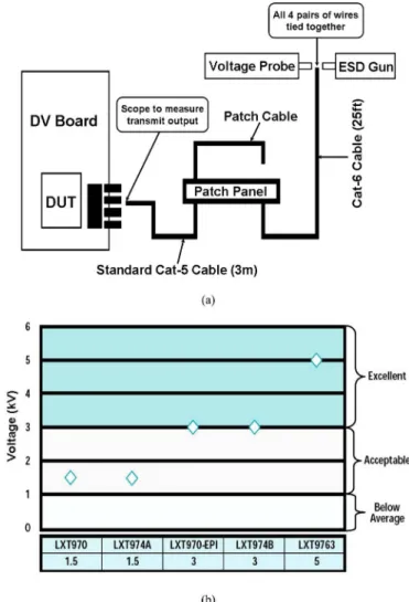
In order to investigate the CDE robustness in an Ethernet local area network (LAN), a test setup was proposed in Fig. 2(a) [5], [6]. First, a standard category-5 cable was connected to an Ethernet transceiver, and then, an unterminated category-6 cable was charged in 500-V increments starting at 1 kV by using an ESD gun. Afterward, the patch cable was inserted directly into the patch panel to examine the CDE robustness of Ethernet transceivers. An Ethernet transceiver “failed” if its transmit signal amplitude is degraded by more than 10%, so it was unable to link, or it experienced destructive latchup.
By utilizing the test setup and procedure in Fig. 2(a), Fig. 2(b) shows the failure voltage levels of Ethernet transceivers under different IC designs and process technologies. The LXT970, a single-port transceiver using a 0.6-µm CMOS technology, has a minimum failure point of 1.5 kV. But the CDE robustness can double when it was fabricated with the addition of an epitaxial layer, such as LXT970-EPI. Similarly, the LXT974A, a four-port transceiver utilizing a 0.6-µm CMOS technology, experiences a performance improvement (from 1.5 to 3 kV) with a redesign of the twisted-pair port (LXT974B). The LXT9763 is a newer six-port transceiver in a 0.35-µm CMOS technology with design techniques to overcome the effects of CDE in an epitaxial layer, which resulted in a failure level of 5 kV (a performance increase of 3.3 times over the first unit tested). This study has clearly illustrated how the effects of CDE can be minimized through process technology and IC design [5], [6].
B. Discharge Between LAN Cabling and Equipment
The Telecommunication Industry Association (TIA) has pro-posed an equipment to measure CDE discharge waveforms of unshielded twisted-pair (UTP) cables [7], [8]. An HBM ESD gun with a discharge network composed of 150-pF capacitor and 300-Ω resistor, following the International Electrotechnical Commission (IEC) 61000-4-2 Standard [13], was used to inject an 8-kV contact discharge pulse into a conductor pair of an as-sortment of category-5, category-5e, and category-6 UTP cables with a length of 56 m. After the UTP cables are charged, their
Fig. 2. (a) Test setup used to measure and analyze CDE in an Ethernet network [5]. (b) CDE voltage levels of Ethernet transceivers under different IC designs and process technologies [5].
discharge waveforms with unused pairs connected together and grounded have been measured and shown in Fig. 3 [7]. The cor-responding diagram of the measurement setup is also depicted in the inset of Fig. 3. From the measured results, the discharge properties among these UTP cables are not obviously differ-ent because the dielectric materials and capacitances associated with category-5, category-5e, and category-6 cables are almost the same. Moreover, the pulsewidths of all discharge currents of these UTP cables are approximately 475 ns. The pulsewidth of discharge current in the CDE should be proportional to the length of cable under test. It will be greater than 475 ns if a longer cable is used. Such a pulsewidth provides a way for us to find an efficient component-level measurement method for investigating the CDE robustness of I/O devices in IC products. In this paper, an LP-TLP system was built up with a current pulsewidth of 500 or 1000 ns, which can simulate the current pulse of the CDE with the corresponding cable length.
III. LP-TLP MEASUREMENTSETUP
In order to reduce the design cycle time for ESD protec-tion circuits, the TLP system has been proposed to measure the
812 IEEE TRANSACTIONS ON ELECTROMAGNETIC COMPATIBILITY, VOL. 50, NO. 4, NOVEMBER 2008
Fig. 3. Cable discharge waveforms when unused pairs are connected together and grounded [7].
snapback I–V characteristics and the secondary breakdown cur-rent (It2) of CMOS devices [14]–[16]. The TLP system pro-vides a single and continually increasing voltage pulse to the device under test (DUT). The pulsewidth is as short as 100 ns to simulate the HBM ESD stress. From the equivalent circuit for an HBM ESD model, the 1500-Ω resistor is in series with the impendence of the DUT (Rdevice), so the peak HBM cur-rent (IESD) equals to VESD/(1500 Ω + Rdevice). The earlier publications have reported the value of the secondary break-down current (It2) close to the value of the peak HBM current (IESD) [17], [18]. Thus, the relationship between the secondary breakdown current (It2) and the HBM ESD level (VESD) can be approximated as
VESD≈ (1500 Ω + Rdevice)× It2 (1) where Rdeviceis the snapback turn-on resistance of the DUT. Be-cause the relation between the secondary breakdown current and the HBM ESD level of protection devices is a linear function, the TLP system has been widely used to evaluate the component-level HBM ESD robustness of CMOS devices [17]–[19]. A. Measurement Setup of the Proposed LP-TLP
By using the well-known characteristics of the TLP system, in this paper, the LP-TLP system is proposed to evaluate CDE behavior of silicon devices and integrated circuits. The pro-posed LP-TLP system with two kinds of long pulsewidths (500 ns/1000 ns) is different from the traditional TLP sys-tem with a short pulsewidth of 100 ns. The LP-TLP syssys-tem with a pulsewidth of 500 ns is consistent with the pulsewidths (∼475 ns) of CDEs shown in Fig. 3. Thus, the LP-TLP sys-tem can be utilized to examine damage to a DUT under CDE stress. Fig. 4(a) and (b) represents the measurement setups for the traditional TLP test and the proposed LP-TLP test, respec-tively. In order to simulate CDE-like pulsewidth, the length of
Fig. 4. Measurement setups. (a) Traditional TLP test. (b) Proposed LP-TLP test.
the transmission line for the proposed LP-TLP test is increased to five times or ten times longer than that of the traditional TLP test. The measurement setups includes a diode, a load resis-tance (RL), a 10-m transmission line for the traditional TLP
test, a 50-m transmission line (or a 100-m transmission line) for the proposed LP-TLP test, two switches (SW1 and SW2), a high-voltage dc supply, a current probe, a voltage probe, and an oscilloscope.
The diode and the load resistance (RL) are connected at the
polarization end to absorb the reflection wave. The principle of LP-TLP operation is described as follows. In the initial state, the switch SW1 is short circuit and the switch SW2 is open circuit. Through the high-voltage resistance RH, the high-voltage dc
supply provides the transmission line with a fixed voltage. The switch SW1 is an open circuit and the switch SW2 is a short circuit in the next state. The stored energy on the transmission line transfers to the DUT, and then, the current and voltage pulses on the DUT are measured by the oscilloscope to obtain the first group of data of the LP-TLP-measured I−V curve. Afterward, the switch SW1 returns to a short circuit and the switch SW2 reverts to an open circuit. Through the high-voltage resistance RH, the high-voltage dc supply provides the transmission line
with a higher fixed voltage. The second group of current/voltage data is measured by repeating the aforementioned steps. The foregoing procedures are continuously duplicated until all I−V characteristics are measured. However, a permanent damage happens when the DUT is overheated. With the aid of the LP-TLP system, the secondary breakdown point of semiconductor devices under CDE stress can be measured.
B. Verification on LP-TLP With a 50-Ω Load Resistor and Gate-Grounded NMOS (GGNMOS)
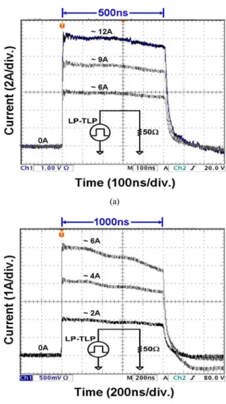
A 50-Ω resistor is used as the DUT to verify that the LP-TLP system can generate a long current pulse similar to a cable discharge waveform. The LP-TLP-measured current waveforms are shown in Fig. 5(a) and (b). In Fig. 5(a), when a 50-m trans-mission line is charged to 450, 640, and 880 V by the high-voltage dc supply, it will generate the corresponding LP-TLP currents of 6, 9, and 12 A, respectively, into the 50-Ω resistor at the DUT. So, the amplitude of the current pulse is obviously in-creased while the charged voltage provided by the high-voltage dc supply is increased. Furthermore, the pulsewidth of these three current waveforms is 500 ns when the length of the trans-mission line is 50 m, so the proposed LP-TLP system with a long current pulsewidth has been proven. If the length of the long-pulse transmission line in the LP-TLP setup is 100 m, the generated current waveform has a pulsewidth of 1000 ns, as shown in Fig. 5(b). The current pulsewidth is a function of the cable length of transmission line in the LP-TLP setup.
A gate-grounded NMOS (GGNMOS) device, which has been widely used as the on-chip ESD protection device in CMOS ICs, is regarded as the DUT to demonstrate that the LP-TLP system can accurately measure its snapback characteristics and sec-ondary breakdown current (It2). The 500- and 1000-ns LP-TLP-measured I−V characteristics of a GGNMOS with a device dimension of W /L = 240 µm/0.3 µm are shown in Fig. 6(a). In addition, Fig. 6(b)–(g) exhibits the time-domain I−V wave-forms of a GGNMOS device under 500-ns LP-TLP stress at the corresponding points marked in Fig. 6(a). The I−V curves of the GGNMOS device will shift from the initial point A to the trigger point B as the high-voltage dc supply continuously pro-vides higher energy. After passing through the trigger point B, the I−V curve will enter the snapback region because the par-asitic lateral bipolar junction transistor (BJT) in the GGNMOS
Fig. 5. (a) 500-ns and (b) 1000-ns LP-TLP current waveforms on a 50-Ω resistor under different charged voltages.
device is turned on. The point C and the point D are the initial point and the middle point in the snapback region, respectively. Subsequently, the curve will reach the critical point E, called the secondary breakdown point of the GGNMOS device. Further-more, the corresponding current of the secondary breakdown point is named the secondary breakdown current (It2). If the high-voltage dc supply further raises the charged voltage, the I−V curve will reach the point F into the secondary breakdown region, which causes permanent damage to the GGNMOS de-vice. Here, the failure criterion of silicon devices is defined as when the leakage current of the DUT exceeds 1 µA after the 500-ns LP-TLP stress. From the measured results, the 500-ns LP-TLP system can efficiently measure the snapback character-istics of a GGNMOS device under CDE-like stress. Fig. 6(a) shows that the 500-ns LP-TLP-measured trigger voltage is 5.9 V, the snapback voltage is 4.3 V, and It2 is 2.3 A.
Fig. 7(a)–(f) shows the time-domain I−V waveforms of a GGNMOS device under 1000-ns LP-TLP stress at the corre-sponding points marked in Fig. 6(a). Similarly, the 1000-ns
814 IEEE TRANSACTIONS ON ELECTROMAGNETIC COMPATIBILITY, VOL. 50, NO. 4, NOVEMBER 2008
Fig. 6. (a) Measured I−V characteristics of a GGNMOS device by the proposed 500- and 1000-ns LP-TLP. (b)–(g) Measured time-domain I−V waveforms of a GGNMOS device under 500-ns LP-TLP stress at the corresponding points marked in (a).
Fig. 7. (a)–(f) Measured time-domain I−V waveforms of a GGNMOS device under 1000-ns LP-TLP stress at the corresponding points marked in Fig. 6(a).
LP-TLP system can also measure and analyze the secondary breakdown characteristic of a GGNMOS device. As shown in Fig. 6(a), the trigger voltage, the snapback voltage, and It2 under the 1000-ns LP-TLP stress are 5.9 V, 4.3 V, and 1.7 A, respectively. From the aforementioned tests, the 500-ns (1000 ns) LP-TLP system can be used to effectively observe the CDE robustness of a DUT.
IV. DEPENDENCE OFCDE ROBUSTNESS ONLAYOUT
PARAMETERS OFCMOS DEVICES
In order to design area-efficient CDE protection circuits, the CDE robustness of protection devices is considered as a function
of layout area. To optimize the layout area, the layout spacings are the major considerations for designing CDE robust devices. The main layout factors to affect effectiveness of CDE protection devices are the channel width (W ), the channel length (L), the finger width (Wf) of each finger, the spacing from source contact to polygate edge (Z), and the silicide-blocking (SAB) width (X), which are illustrated in Fig. 8 (note: the SAB layer is the silicide-blocking layer to block the silicided diffusion on the drain regions). Moreover, the descriptions for different layout parameters are shown in Table I. When the dependence of CDE current paths on the layout parameters are well comprehended, CDE protection devices can be optimized to yield higher CDE robustness.
816 IEEE TRANSACTIONS ON ELECTROMAGNETIC COMPATIBILITY, VOL. 50, NO. 4, NOVEMBER 2008
Fig. 8. Layout top view of a finger-type GGNMOS device with different layout parameters.
TABLE I
DESCRIPTIONS FORDIFFERENTLAYOUTPARAMETERS IN ATRANSISTORLAYOUT
The dependence of these five layout factors on the CDE level for GGNMOS and gate-voltage drain drain (VDD) PMOS (GDPMOS) are investigated practically through fabricated sil-icon chips in a 0.18-µm-salicided CMOS process. To clearly understand the protection device differences between the CDE and the HBM ESD, the proposed LP-TLP and the conventional TLP-measured data are compared to find the dependence on layout parameters.
A. Channel Width
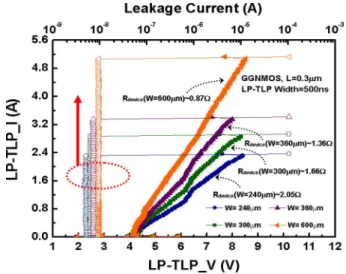
The 500-ns LP-TLP-measured I−V characteristics, the cor-responding leakage currents, and the turn-on resistances of GGNMOS devices with different channel widths, but with the same channel length and unit-finger width, are shown in Fig. 9. From the measured results, all GGNMOS devices with different channel widths have distinct snapback characteristics. In addi-tion, the It2 of the GGNMOS device is linearly increased with increasing the channel width. The It2 levels of GGNOS devices with different widths of 240, 300, 360, and 600 µm under the proposed 500-ns LP-TLP test are 2.3, 2.9, 3.3, and 5.1 A, re-spectively. But the turn-on resistance of the GGNMOS device in the snapback region is decreased with increasing channel width. Here, the turn-on resistance is defined as the voltage variation
Fig. 9. 500-ns LP-TLP-measured I−V characteristics and the leakage cur-rents of GGNMOS devices with different channel widths.
over current variation before second breakdown in the 500-ns LP-TLP-measured I−V curve. The turn-on resistance can be expressed as
Rdevice ≡
∂VD S
∂ID
. (2)
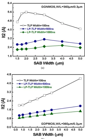
The turn-on resistances of GGNOS devices with different widths of 240, 300, 360, and 600 µm under the proposed 500-ns LP-TLP test are 2.05, 1.66, 1.36, and 0.87 Ω, respectively. The dependence of the It2 levels of the GGNMOS and GDPMOS devices on the channel width under the traditional 100-ns TLP and the proposed 500-ns (1000-ns) LP-TLP tests is shown in Fig. 10(a) and (b), respectively. The unit-finger width (Wf) of the GGNMOS and GDPMOS devices in the finger-type layout is kept at 30 µm. For both GGNMOS and GDPMOS devices, the channel length (L), the SAB width (X), the clearance from SAB to polygate edge (Y ), the spacing from source contact to polygate edge (Z), and the distance from drain diffusion to guard ring edge (G) are drawn as 0.3, 3, 0.3, 0.75, and 2 µm, respec-tively. In Fig. 10(a), these It2 levels of the GGNMOS devices are linearly increased when the channel width is increased. Besides, the It2 levels of GGNMOS devices under the traditional 100-ns TLP test are much higher than those under the proposed 500-ns (1000 ns) LP-TLP test. For instance, the It2 of the GGNMOS device with a channel width of 360 µm under the traditional 100-ns stress is 5.3 A, but that with the same device dimension and layout style under the proposed 500-ns (1000 ns) LP-TLP test is only 3.4 A (2.4 A). Similarly, when the channel width is increased, the It2 levels of the GDPMOS devices under the traditional 100-ns TLP and the proposed 500-ns (1000 ns) LP-TLP tests are all increased, as shown in Fig. 10(b). Furthermore, under the same device dimensions and layout style, the It2 levels of the GDPMOS devices under 500-ns (1000 ns) LP-TLP stress are evidently lower than those under the traditional 100-ns TLP stress. Attributed to the longer LP-TLP pulsewidth, the stronger energy is injected into the DUT device, which causes reduced robustness of the device to CDE stress.
Fig. 10. Dependence of the It2 of (a) GGNMOS and (b) GDPMOS devices on the channel width under the traditional 100-ns TLP and the proposed 500-ns (1000 ns) LP-TLP tests.
B. Channel Length
The relations between the channel length and the It2 levels of the GGNMOS and GDPMOS devices under the traditional 100-ns TLP and the proposed 500-ns (1000 ns) LP-TLP tests are illustrated in Fig. 11(a) and (b), respectively. The layout style and other parameters are all kept the same (W = 360 µm, Wf = 30 µm, X = 3 µm, Y = 0.3 µm, Z = 0.75 µm, and G = 2 µm), but only the channel length is different in this investigation. From the measured results in Fig. 11(a), when the GGNMOS device has a short enough channel length under the traditional 100-ns TLP test, the efficiency and performance of the parasitic lateral BJT in the GGNMOS device is signifi-cantly improved [20]. Therefore, the GGNMOS device with a short channel length (0.25 µm) can withstand a much higher HBM ESD level than that with a medium channel length of ∼0.35 µm. However, the GGNMOS device with a shorter chan-nel length under the proposed 500-ns LP-TLP test has a lower It2, especially for a channel width of 0.25 µm. The It2 levels of the GGNMOS devices for the proposed 1000-ns LP-TLP test
Fig. 11. Dependence of the It2 of (a) GGNMOS and (b) GDPMOS devices on the channel length under the traditional 100-ns TLP and the proposed 500-ns (1000 ns) LP-TLP tests.
are the lowest and not obviously varied by different channel lengths. Similarly, the It2 levels of the GGNMOS devices for the traditional 100-ns TLP test are still higher than those for the 500-ns (1000 ns) LP-TLP test.
On the contrary, the GDPMOS device with a shorter chan-nel length has a lower It2 under the traditional 100-ns TLP and 500-ns (1000 ns) LP-TLP tests, as shown in Fig. 11(b). Even for the GDPMOS device with a channel length of only 0.25 µm, its It2 levels under the traditional 100-ns TLP test and the 500-ns (1000 ns) LP-TLP tests are only 2.2 and 1.18 A (0.95 A), respectively, because the turn-on efficiency of lateral p-n-p BJT in the GDPMOS device is not improved. From this experimental investigation, the selection of MOSFET for ESD and CDE protection is quite different in the 0.18-µm-salicided CMOS process.
C. Unit-Finger Width
In the I/O cell layout of CMOS ICs, a large-dimension de-vice is traditionally drawn with multiple fingers in a parallel
818 IEEE TRANSACTIONS ON ELECTROMAGNETIC COMPATIBILITY, VOL. 50, NO. 4, NOVEMBER 2008
Fig. 12. Dependence of the It2 of (a) GGNMOS and (b) GDPMOS devices on the unit-finger width under the traditional 100-ns TLP and the proposed 500-ns (1000 ns) LP-TLP tests.
connection. If the finger width (Wf) of every finger is shorter, more fingers must be used to form the same large-dimension de-vice. The large-dimension device with different numbers of unit fingers and unit-finger widths can cause different ESD and CDE performances, even though the devices have the same channel width (W ) and channel length (L) dimensions. The multiple fingers of a large-dimension device are hard to uniformly turn on during the ESD and CDE stresses; hence, they may result in different ESD and CDE levels. To verify this issue, both the GGNMOS and GDPMOS devices with a fixed channel width (W )/channel length (L) of 360 µm/0.3 µm, but different unit-finger widths, are investigated under the traditional 100-ns TLP and the 500-ns (1000 ns) LP-TLP tests. The tested results are shown in Fig. 12(a) and (b).
From the measured results, the It2 of the GGNMOS de-vices of W = 360 µm under the traditional 100-ns TLP stress is decreased from 5.61 to 4.46 A as the GGNMOS device is drawn with the finger number increased from 8 to 24. When the GGNMOS device is drawn with the finger number increased
Fig. 13. Dependence of the It2 of (a) GGNMOS and (b) GDPMOS devices on the spacing from source contact to polygate edge under the traditional 100-ns TLP and the proposed 500-ns (1000 ns) LP-TLP tests.
from 8 to 24, the It2 levels of the GGNMOS devices of W = 360 µm under the proposed 500 ns (1000 ns) LP-TLP stress are increased from 2.94 to 3.39 A (2.22–2.56 A). Sim-ilarly, the larger finger number in the GDPMOS device leads to a slightly lower ESD and CDE robustness. From the earlier analysis, the implication is that the finger-type GGNMOS and GDPMOS devices with shorter finger widths cannot be uni-formly turned on during ESD and CDE stresses. Moreover, the CDE robustness of GGNMOS and GDPMOS devices is much worse than their HBM ESD robustness under the same layout factor for a given unit-finger width.
D. Spacing From Source Contact to Polygate Edge
The relationships between the spacing from the source con-tact to the poly-gate edge (Z) and the It2 levels of GGNMOS and GDPMOS devices under the traditional 100-ns TLP and the proposed 500-ns (1000 ns) LP-TLP tests are investigated in Fig. 13(a) and (b), respectively. In this investigation, all the
layout style and other spacings are kept the same (W = 360 µm, L = 0.3 µm, Wf = 30 µm, X = 3 µm, Y = 0.3 µm, and G = 2 µm), but only the spacing Z is varied from 0.25 to 2 µm in the test chips. From the experimental results, the varied spacing Z only causes a slight variation on the It2 from 5.14 to 5.25 A (2.12–2.47 A) in the GGNMOS (GDPMOS) device un-der the traditional 100-ns TLP stress. Unun-der the proposed 500-ns LP-TLP stress, the It2 of GGNMOS (GDPMOS) is increased from 2.88 to 3.34 A (1.13–1.39 A) as the spacing Z is increased from 0.25 to 2 µm. However, the GGNMOS device with a shorter spacing Z under the proposed 500-ns LP-TLP stress has a lower It2 current, especially for the spacing of 0.25 µm. In addition, it also results in a small increase of It2 from 2.3 to 2.74 A (0.9–1.16 A) of GGNMOS (GDPMOS) device for the proposed 1000-ns LP-TLP stress when the spacing Z is varied. Therefore, the spacing Z has no obvious impact on the ESD and CDE robustness ofMOSFET.
E. SAB Width
The dependence of the It2 levels of the GGNMOS and GDPMOS devices on the SAB width (X) under the tradi-tional 100-ns TLP and the proposed 500-ns (1000 ns) LP-TLP tests is shown in Fig. 14(a) and (b), respectively. The layout style and other clearances are all kept the same (W = 360 µm, L = 0.3 µm, Wf = 30 µm, Y = 0.3 µm, Z = 0.75 µm, and G = 2 µm), but only the SAB width is different in this inves-tigation. In Fig. 14(a), the It2 of GGNMOS device under the traditional 100-ns TLP stress is increased as the SAB width is increased from 1.5 to 2 µm. Because the SAB on the drain region introduces ballast resistance, it could limit ESD currents to flow through the channel surface of theMOSFET. On the contrary, when the SAB width is increased from 2 to 5 µm, the It2 of the GGNMOS device under the traditional 100-ns TLP test is de-creased from 5.6 to 4.1 A. Due to the large increase of the SAB width (i.e., too much SAB added), the power consumption along the ESD current path increases, resulting in a higher thermal stress, and consequently, a significantly lower It2. From the 100-ns TLP-measured results, the maximum It2 of the GGNMOS device is for the SAB width of 2 µm. Under the proposed 500-ns (1000 ns) stress, the It2 trend of the GGNMOS device is simi-lar to the case under the traditional 100-ns TLP stress but with much lower current levels. However, the maximum It2 levels of the GGNMOS device under the 500-ns (1000 ns) LP-TLP test are for the SAB width of 3 and 4 µm, respectively, as shown in Fig. 14(a).
In contrast, in Fig. 14(b), the It2 levels of the GDP-MOS device for the traditional 100-ns TLP and the proposed 500-ns (1000 ns) LP-TLP stresses are all increased when the SAB width is increased from 0.75 to 5 µm. This phenomenon resulted from the existence of ballast resistance, which causes higher HBM ESD and CDE robustness [21], [22]. From the experimental investigations, it is evident that the GGNMOS and GDPMOS protection devices are too weak to withstand such CDE-induced high energy. Consequently, the It2 levels of CMOS devices for the 500-ns (1000 ns) LP-TLP stress
Fig. 14. Dependence of the It2 of (a) GGNMOS and (b) GDPMOS devices on the SAB width under the traditional 100-ns TLP and the proposed 500-ns (1000 ns) LP-TLP tests.
are much lower than those for the traditional 100-ns TLP stress.
F. Power-to-Failure Mechanism
Fig. 15(a) shows the It2 of the GGNMOS device (W /L = 360 µm/0.3 µm) as a function of the pulsewidth (τ ) of the stress. From the slope in Fig. 15(a), the It2 of the GGNMOS device is of the order of ∼−1/3 to the pulsewidth (τ) of the stress. The power to failure (defined as Vt2× It2, Vt2 = the voltage at secondary breakdown point) of the GGNMOS device (W/L = 360 µm/0.3 µm) as a function of the pulsewidth of the stress is shown in Fig. 15(b), where the power to failure is found to be of the order of ∼−1/2 to the pulsewidth (τ) of the stress. The results confirmed that the power to failure of the GGNMOS device is decreased when the pulsewidth is increased. This tendency, observed in Fig. 15, is fully consistent with the Wunsch–Bell law [23].
820 IEEE TRANSACTIONS ON ELECTROMAGNETIC COMPATIBILITY, VOL. 50, NO. 4, NOVEMBER 2008
Fig. 15. Dependence of (a) secondary breakdown current (It2) and (b) power-to-failure (defined as Vt2× It2) on the pulsewidth (τ ) of TLP stress.
G. Failure Analysis
Fig. 16(a)–(c) reveals the SEM photographs of the GGNMOS device (W/L = 420 µm/0.3 µm) to observe the fail-ure locations after the traditional 100-ns TLP test and the pro-posed 500-ns (1000 ns) LP-TLP test. As shown in Fig. 15(a), the failure locations are uniformly distributed among all fingers for the traditional 100-ns TLP test. Fig. 15(b) shows an obvious local failure region because the GGNMOS device is directly burned out from drain to common source in two fingers after the proposed 500-ns LP-TLP test. After the proposed 1000-ns LP-TLP test, not only is a local damage site seriously burned out from drain to source in one finger, but also an adjacent drain contact region failed due to a pinhole, as shown in Fig. 15(c). From these SEM pictures, the fingers in the GGNMOS de-vice cannot be uniformly turned on during the proposed 500-ns (1000 ns) LP-TLP stress because of the CDE-induced higher pulse energy. This causes an evident reduction in the It2 of the GGNMOS device under CDE. By using the proposed 500-ns (1000 ns) LP-TLP test, one set of optimized design rules against CDE stress on chip layout in IC products can be established in a given CMOS process.
Fig. 16. SEM photographs on the GGNMOS device (W/L = 420 µm/ 0.3 µm) to observe its failure locations after (a) the traditional 100-ns TLP test, (b) the proposed 500-ns TLP test, and (c) the proposed 1000-ns LP-TLP test.
V. CONCLUSION
The proposed LP-TLP system can be used to find the op-timized design rules for CDE protection in CMOS ICs. The dependence of CDE robustness on layout spacings of CMOS devices in the salicided CMOS process has been investigated and discussed in detail. Generally, the device with a wider chan-nel width, a longer chanchan-nel length, a wider unit finger width, a larger SAB width, a wider spacing from source contact to polygate edge, a larger clearance from SAB to polygate edge, and a far distance from drain diffusion to guard ring edge leads to a higher CDE robustness. From the measured results, the It2 levels of the GGNMOS and GDPMOS devices for the proposed 500-ns (1000 ns) LP-TLP test are much lower than those for the traditional 100-ns TLP test. Therefore, CDE has been confirmed to cause a significant degradation in the reliability of ESD only-protected IC products. Furthermore, the gate oxide is becoming much thinner when the CMOS process is scaled down to 0.13, 90, and 65 nm processes. It will be a more severe challenge to provide effective CDE protection for IC products fabricated in such advanced CMOS technology. By using the proposed LP-TLP system, one set of design rules for I/O devices to obtain high CDE robustness in a given CMOS process can be evaluated and built up for chip layout.
REFERENCES
[1] W. Stadler, T. Brodbeck, R. Gaertner, and H. Gossner, “Cable discharges into communication interfaces,” in Proc. EOS/ESD Symp., 2006, pp. 144– 151.
[2] K. Chatty, P. Cottrell, R. Gauthier, M. Muhammad, F. Stellari, A. Weger, P. Song, and M. McManus, “Model-based guidelines to suppress cable discharge event (CDE) induced latchup in CMOS ICs,” in Proc. IEEE Int.
[3] C. J. Brennan, K. Chatty, J. Sloan, P. Dunn, M. Muhammad and R. Gauthier, “Design automation to suppress cable discharge event (CDE) induced latchup in 90-nm CMOS ASICs,” in Proc. EOS/ESD Symp., 2005, pp. 126–130.
[4] R. Brooks. (2001, Mar.). A simple model for a cable discharge
event, IEEE 802.3 Cable Discharge Ad-hoc. [Online]. Available:
http://www.ieee802.org/3/ad_hoc/copperdis/public/docs/cable_discharge _model1.pdf.
[5] J. Deatherage and D. Jones. (2000, Dec.). Multiple factors trigger cable dis-charge events in ethernet LANs. Electron. Des. [Online]. 48(25), pp. 111– 116. Available: http://electronicdesign.com/Articles/Index.cfm?ArticleID =4991&pg=2
[6] Intel Corporation, “Cable discharge event in local area network environ-ment,” White Paper, Order No: 249812-001, Jul. 2001.
[7] Cabling ESD Study, IEEE 802.3 Cable Discharge Ad-hoc. (2001, Mar.). [Online]. Available: http://grouper.ieee.org/groups/802/3/ ad_hoc/copperdis/public/docs/Cabling_ESD_Study.pdf
[8] Category 6 Cabling: Static Discharge Between LAN Cabling and Data
Terminal Equipment, Category 6 Consortium, Telecommunications
In-dustry Association (TIA), EIA/JEDEC Standard, Dec. 2002.
[9] H. Geski, “DVI compliant ESD protection to IEC 61000-4 2 level 4 Standard,” Conformity, pp. 12–17, Sep. 2004.
[10] IC Latch-Up Test, Electronic Industries Association, EIA/JEDEC Stan-dard 78, 1997.
[11] M.-D. Ker and T.-X. Lai, “Method to evaluate cable discharge event (CDE) reliability of integrated circuits in CMOS technology,” in Proc. IEEE Int.
Symp. Quality Electron. Des., 2006, pp. 597–602.
[12] M.-D. Ker and T.-X. Lai, “Dependence of layout parameters on CDE (ca-ble discharge event) robustness of CMOS devices in a 0.25-µm salicided CMOS process,” in Proc. IEEE Int. Rel. Phys. Symp, San Jose, CA, Mar. 2006, pp. 633–634.
[13] Electromagnetic Compatibility (EMC)—Part 4—2: Testing and
Measure-ment Techniques—Electrostatic Discharge Immunity Test, International
Standard IEC 61000-4-2, 1995.
[14] T. J. Maloney and N. Khurana, “Transmission line pulsing techniques for circuit modeling of ESD phenomena,” in Proc. EOS/ESD Symp., 1985, pp. 49–54.
[15] R. Ashton, “Modified transmission line pulse system and transistor test structures for the study of ESD,” in Proc. IEEE Int. Conf. Microelectron.
Test Struct., Nara, Japan, Mar. 22–25, 1995, vol. 8, pp. 127–132.
[16] J. C. Lee, R. Young, J. J. Liou, G. D. Croft, and J. C. Bernier, “An improved transmission line pulsing (TLP) setup for electrostatic discharge (ESD) testing in semiconductor devices ICs,” in Proc. IEEE Int. Conf.
Microelectron. Test Struct., Kobe, Japan, 2001, vol. 14, pp. 233–238.
[17] J. Barth, K. Verhaege, L. G. Henry, and J. Richner, “TLP calibration, correction, standards, and new techniques,” IEEE Trans. Electron. Packag.
Manuf., vol. 24, no. 2, pp. 99–108, Apr. 2001.
[18] S. G. Beebe, “Methodology for layout design and optimization of ESD protection transistors,” in Proc. EOS/ESD Symp., 1996, pp. 265–275. [19] C. H. Diaz, T. E. Kopley, and P. J. Marcoux, “Building-in ESD/EOS
reliability for sub-halfmicron CMOS process,” in Proc. IEEE Int. Rel.
Phys. Symp., Las Vegas, NV, Apr. 4–5, 1995, pp. 276–283.
[20] T.-Y. Chen and M.-D. Ker, “Analysis on the dependence of layout param-eters on ESD robustness of CMOS devices for manufacturing in deep-submicron CMOS process,” IEEE Trans. Semicond. Manuf., vol. 16, no. 3, pp. 486–500, Aug. 2003.
[21] G. Notermans, A. Heringa, M. Van Dort, S. Jansen, and F. Kuper, “The effect of silicide on ESD performance,” in Proc. IEEE Int. Rel. Phys.
Symp., San Diego, CA, 1999, pp. 154–158.
[22] J. Li, D. Alvarez, K. Chatty, M. Abou-Khalil, R. Gauthier, C. Russ, C. Seguin, and R. Halbach, “Analysis of failure mechanism on gate-silicided and gate-non-silicided, drain/source silicide-blocked ESD NMOSFETs in a 65 nm bulk CMOS technology,” in Proc. IEEE Int. Symp.
Phys. Failure Anal. Intergraded Circuits, Singapore, Jul. 2006, pp. 276–
280.
[23] D. C. Wunsch and R. R. Bell, “Determination of threshold voltage levels of semiconductor diodes and transistors due to pulsed voltages,” IEEE
Trans. Nucl. Sci., vol. NS-15, no. 6, pp. 244–259, Dec. 1968.
Ming-Dou Ker (S’92–M’94–SM’97–F’08) received
the Ph.D. degree from the Institute of Electronics, National Chiao-Tung University, Hsinchu, Taiwan, R.O.C., in 1993.
He was a Department Manager in the Very-Large-Scale Integration (VLSI) Design Division of the Computer and Communication Research Laborato-ries (CCLs), Industrial Technology Research Institute (ITRI), Taiwan. Since 2004, he has been a Full Pro-fessor in the Department of Electronics Engineering, National Chiao-Tung University. During 2006–2008, he served as the Director of Master Degree Program in the College of Electrical Engineering and Computer Science, National Chiao-Tung University, as well as the Associate Executive Director of the National Science and Technology Pro-gram on System-on-Chip (NSoC Office), Taiwan. In 2008, he moved to I-Shou University, Kaohsiung, Taiwan, as a Chair Professor and the Vice President. He had been invited to teach and/or to consult reliability and quality design for integrated circuits by hundreds of design houses and semiconductor companies in the worldwide IC industry. He is the author or coauthor of more than 300 technical papers published in various international journals and conferences in the field of reliability and quality design for circuits and systems in CMOS tech-nology. He is the inventor or co-inventor of 135 U.S. patents and 142 Taiwan patents. His current research interests include reliability and quality design for nanoelectronics and gigascale systems, high-speed and mixed-voltage I/O inter-face circuits, on-glass circuits for system-on-panel applications, and biomimetic circuits and systems for intelligent prosthesis.
Prof. Ker was a member of the Technical Program Committee and Session Chair of numerous international conferences. He was an Associate Editor of the IEEE TRANSACTIONS ONVERYLARGESCALEINTEGRATIONSYSTEMS. He has been selected as the Distinguished Lecturer in the IEEE Circuits and Systems Society (2006–2007) and the IEEE Electron Devices Society (since 2008). He was the President of the Foundation of Taiwan Electrostatic Discharge (ESD) Association. In 2005, he was awarded with the National Invention Award in Taiwan for one of his patents on ESD protection design.
Tai-Hsiang Lai received the B.S. degree in 2004
from the Department of Electrical Engineering, Yuan Ze University, Taoyuan, Taiwan, R.O.C., and the M.S. degree in 2006 from the Institute of Elec-tronics, National Chiao-Tung University, Hsinchu, Taiwan, where he is currently working toward the Ph.D. degree.
During 2006, he was a Senior Engineer in the Electrostatic Discharge (ESD) Engineering Depart-ment, Reliability Technology and Assurance Divi-sion, United Microelectronic Corporation (UMC). His current research interests include ESD and latchup protection designs for high-voltage (HV) and smart power technologies.
![Fig. 3. Cable discharge waveforms when unused pairs are connected together and grounded [7].](https://thumb-ap.123doks.com/thumbv2/9libinfo/7658235.140104/3.891.198.695.101.443/fig-cable-discharge-waveforms-unused-pairs-connected-grounded.webp)