IEEE ELECTRON DEVICE LETTERS, VOL. 22, NO. 6, JUNE 2001 269
High-Performance Low-Temperature Poly-Si TFTs
Crystallized by Excimer Laser Irradiation with
Recessed-Channel Structure
Ching-Wei Lin, Li-Jing Cheng, Yin-Lung Lu, Yih-Shing Lee, and Huang-Chung Cheng, Member, IEEE
Abstract—High-performance low-temperature poly-Si (LTPS)
thin-film transistors (TFTs) have been fabricated by excimer laser crystallization (ELC) with recessed-channel (RC) structure. The TFTs made by this method possessed large longitudinal grains in the channel regions, therefore, they exhibited better electrical char-acteristics as compared with the conventional ones. The average field-effect mobility above 300 cm2/V-s and on/off current ratio higher than 109 were achieved in these RC-structure devices. In addition, since grain growth could be artificially controlled by this method, the device electrical characteristics were less sensitive to laser energy density variation, and therefore the uniformity of de-vice performance could be improved.
Index Terms—Excimer laser crystallization (ELC), re-cessed-channel (RC), thin-film transistor (TFT).
I. INTRODUCTION
L
OW-TEMPERATURE poly-Si (LTPS) thin-film transis-tors (TFTs) fabricated by excimer laser crystallization (ELC) have been widely studied for AMLCD applications [1]–[3]. Although high-performance LTPS TFTs with mobility over 300 cm /V-s have been made by ELC, the laser annealing conditions had to be precisely controlled near the super lateral growth (SLG) region to acquire poly-Si thin film with large grains [4]–[6]. As a result, narrow process window and poor uniformity of device performance were exhibited in ELC LTPS TFTs. Although many methods have been proposed to solve the above problems by artificially controlling grain growth, such as the SLS process [7], shaping the laser beam [8], and capping reflective or anti-reflective layer [9], they always imposed some complexities on device fabrication process or were not easy to implement.From the viewpoint of TFTs performance, devices with thinner active layer exhibit better electrical characteristics [10], [11]. However, for thin film crystallized by excimer laser annealing, as film thickness is reduced, the average grain size of the thin film crystallized at the optimal laser energy density may become smaller due to faster quenching rate of the thinner ones [12], [13]. Moreover, devices with thinner film
Manuscript received January 23, 2001; revised March 15, 2001. This work was supported by the National Science Council, Taiwan, R.O.C., under Contract NSC 89-2215-E-009-108. The review of this letter was arranged by Editor J. Sin. C.-W. Lin, L.-J. Cheng, Y.-L. Lu, and H.-C. Cheng are with the Institute of Electronics, National Chiao Tung University, Hsinchu 300, Taiwan, R.O.C.
Y.-S. Lee is with the Electronics Research and Service Organization, In-dustrial Technology Research Institute, Hsinchu 300, Taiwan, R.O.C. (e-mail: [email protected]).
Publisher Item Identifier S 0741-3106(01)04658-4.
thickness exhibit large source/drain series resistance, which in turn significantly reduces the current drive [14]. As a result, thickness of thin film must be carefully determined in order to optimize the device performance.
In this letter, we adopt the recessed-channel (RC) structure for ELC. The process is simple and large grains can be formed in the thin channel region with this structure. In addition, since the thickness of source/drain region can be made thicker, the series resistance of these devices will not increase significantly, and device performance can be further improved.
II. DEVICEFABRICATION
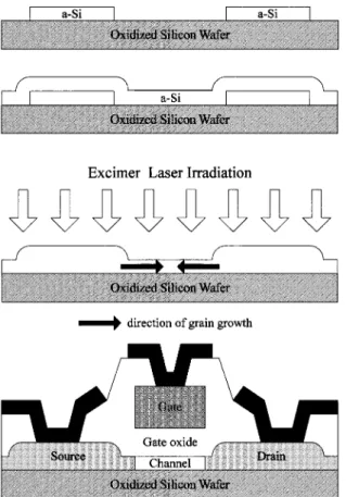
The key processes for fabricating LTPS TFTs crystallized with RC structure are illustrated in Fig. 1. At first, a 50-nm amorphous silicon layer was deposited on an oxidized silicon substrate by LPCVD at 550 C with SiH as gaseous source. Then, the amorphous silicon layer in the channel parts was re-moved following by another 50-nm amorphous silicon layer de-position. Because it was not a self-aligned process, a margin of 0.2 m, limited by layer to layer registration, was given to both sides of gate. Laser crystallization was performed by KrF ex-cimer laser ( nm). During the irradiation, the samples were located on a substrate in a vacuum chamber pumped down to 10 Torr and substrate was maintained at 400 C. After defining the active islands, a 100-nm TEOS gate oxide was de-posited by PECVD at 300 C. A 150-nm amorphous silicon film was then deposited at 550 C by LPCVD for gate electrode. The amorphous silicon and gate oxide were etched by RIE to form gate electrodes. A self-aligned phosphorous implantation with dose of cm was carried out to form source and drain regions. A passivation oxide layer was deposited and the im-planted dopants were activated by thermal annealing at 600 C for 20 h. Contact holes formation and metallization were car-ried out after dopants activation. Finally, TFTs were passivated by 4-h NH plasma treatment to further improve device perfor-mance. For comparison, the conventional ELC LTPS TFTs with a thickness of 50 nm were also fabricated. The laser energy den-sities were optimized for both kinds of device structures.
III. RESULTS ANDDISCUSSION
Fig. 2 shows the SEM photograph of excimer laser crystal-lized poly-Si with RC structure. It is found that large longitu-dinal grains could be artificially grown in the channel region and extend about 1.5 m. It has been reported that lateral thermal
270 IEEE ELECTRON DEVICE LETTERS, VOL. 22, NO. 6, JUNE 2001
Fig. 1. Key processes for fabricating LTPS TFTs crystallized with RC structure.
Fig. 2. SEM photograph of excimer laser crystallized poly-Si with RC structure after Secco etch.
gradient could arise as a result of the heat generated at moving solid-melt interface [15], [16]. Similarly, when a proper laser energy density irradiates the silicon thin film containing dif-ferent thicknesses, the thin region is completely melted while the thick region is only partially melted, leaving behind islands of solid material. As a result, grain growth will come up from the residual, un-melted silicon islands in the thick region, and then stretch toward the completely melted thin channel until small grains, which homogeneously grow in the channel region,
TABLE I
MEASUREDELECTRICALCHARACTERISTICS OFTFTSCRYSTALLIZED WITH DIFFERENTSTRUCTURES
(a)
(b)
Fig. 3. I–V curves of LTPS RC-TFT (solid curves) and conventional TFT (dotted curves) crystallized by excimer laser annealing. (a) Transfer characteristics. (b) Output characteristics.
hinder the extending grains. In this experiment, with laser en-ergy densities between completely melting 50-nm silicon thin film but partially melting the 100-nm one, we got similar re-sults, that is, the process window could be broadened. Since the grain size was less sensitive to laser energy density variation, the device performance exhibited more uniform.
Typical transfer characteristics and output characteristics curves of TFTs crystallized with RC structure and conven-tional one are shown in Fig. 3(a) and (b), respectively. Some important device characteristics are also listed in Table I. Owing to large longitudinal grains growth in the channel regions, TFTs crystallized with RC structure exhibited better
LIN et al.: HIGH-PERFORMANCE LOW-TEMPERATURE POLY-Si TFTs 271
electrical characteristics than the conventional ones, in which the average grain size was about 300 nm. From the 30 TFTs measured, the mobilities of the RC-TFTs ranged from 300 to 350 cm /V-s and on/off current ratios were all more than 10 , but for the conventional TFTs, the mobilities ranged from 70 to 190 cm /V-s. From Fig. 3(b), it is also found that the conventional TFTs with thin channel film suffered current pinching at low drain voltage due to large source/drain series resistance, but the RC-TFTs didn’t encounter this problem. Our measurement of sheet resistance showed that the sheet resistances of 100-nm and 50-nm doped poly-Si thin films were about 880 and 1.8 k , respectively. Such slightly high sheet resistance might be resulted from the low dopant activation efficiency of low-temperature furnace annealing in comparison with laser activation, and would degrade the driving capability of short-channel, high-performance TFTs, especially for the thinner one.
IV. CONCLUSION
High-performance LTPS RC-TFTs have been fabricated by ELC. Because large longitudinal grains could be artificially grown in the thin channel regions accompanying with thick sources/drains for reducing series resistance, the RC-TFTs exhibited better electrical characteristics and uniformity than the conventional ones, and were very suitable for future system-on-panel applications.
REFERENCES
[1] S. D. Brotherton, D. J. McCulloch, J. B. Clegg, and J. P. Gowers, “Ex-cimer-laser-annealed poly-Si thin film transistors,” IEEE Trans. Elec-tron Devices, vol. 40, pp. 407–413, 1993.
[2] G. K. Giust and T. W. Sigmon, “Self-aligned aluminum top-gate polysilicon thin-film transistors fabricated using laser recrystallization and gas-immersion laser doping,” IEEE Electron Device Lett., vol. 18, pp. 394–396, 1997.
[3] A. Kohno, T. Sameshima, N. Sano, M. Sekiya, and M. Hara, “High per-formance poly-Si TFTs fabricated using pulsed laser annealing and re-mote plasma CVD with low temperature processing,” IEEE Trans. Elec-tron Devices, vol. 42, pp. 251–257, Feb. 1995.
[4] J. S. Im and H. J. Kim, “Phase transformation mechanisms involved in excimer laser crystallization of amorphous silicon films,” Appl. Phys. Lett., vol. 63, pp. 1969–1971, 1993.
[5] G. K. Giust, T. W. Sigmon, P. G. Carey, B. Weiss, and G. A. Davis, “Low-temperature polysilicon thin-film transistors fabricated from laser-pro-cessed sputtered-silicon films,” IEEE Electron Device Lett., vol. 19, pp. 343–344, 1998.
[6] G. K. Giust, T. W. Sigmon, J. B. Boyce, and J. Ho, “High-performance laser-processed polysilicon thin-film transistors,” IEEE Electron Device Lett., vol. 20, pp. 77–79, Feb. 1999.
[7] M. A. Crowder, P. G. Carey, P. M. Smith, R. S. Sposili, H. S. Cho, and J. S. Im, “Low-temperature single-crystal Si TFTs fabricated on Si films processed via sequential lateral solidification,” IEEE Electron Device Lett., vol. 19, pp. 306–308, 1998.
[8] C. Oh, M. Ozawa, and M. Matsumura, “A novel phase-modulated ex-cimer-laser crystallization method of silicon thin films,” Jpn. J. Appl. Phys., vol. 37, pp. L492–L495, 1998.
[9] L. Mariucci, R. Carluccio, A. Pecora, V. Foglietti, G. Fortunato, P. Legagneux, D. Pribat, D. Della Sala, and J. Stoemenos, “Lateral growth control in excimer laser crystallized polysilicon,” Thin Solid Films, vol. 337, pp. 137–142, 1999.
[10] S. Zhang, C. Zhu, J. K. O. Sin, J. N. Li, and P. K. T. Mok, “Ultra-thin elevated channel poly-Si TFT technology for fully-integrated AMLCD system on glass,” IEEE Trans. Electron Devices, vol. 47, pp. 569–575, Mar. 2000.
[11] Z. Jin, H. K. Kwok, and M. Wong, “Performance of thin-film transistors with ultrathin Ni-MILC polycrystalline silicon channel layers,” IEEE Electron Device Lett., vol. 20, pp. 167–169, 1999.
[12] S. R. Stiffler and M. O. Thompson, “Transient nucleation following pulsed-laser melting of thin silicon films,” Phys. Rev. B, Condens. Matter, vol. 43, pp. 9851–9855, 1991.
[13] T. Eiumchotchawalit and J. S. Im, “The mechanism of excimer laser-in-duced amorphization of ultra-thin Si films,” Mat. Res. Soc. Symp. Proc., vol. 321, pp. 725–730, 1994.
[14] M. Chan, F. Assaderaghi, S. A. Parke, C. Hu, and P. K. Ko, “Recessed-channel structure for fabricating ultrathin SOI MOSFET with low series resistance,” IEEE Electron Device Lett., vol. 15, pp. 22–24, Jan. 1994. [15] J. S. Im and H. J. Kim, “On the super lateral growth phenomenon
ob-served in excimer laser-induced crystallization of thin Si films,” Appl. Phys. Lett., vol. 64, pp. 2303–2305, 1994.
[16] M. Lee, S. Moon, M. Hatano, K. Suzuki, and C. P. Grigoropoulos, “Re-lationship between fluence gradient and lateral grain growth in spatially controlled excimer laser crystallization of amorphous silicon films,” J. Appl. Phys., vol. 88, pp. 4994–4999, 2000.