新穎三閘極電晶體與薄膜電晶體之製程技術與特性研究
276
0
0
全文
(2) 新穎三閘極電晶體與薄膜電晶體 之製程技術與特性研究. A Study on the Process Technologies and Characteristics of Novel Tri-Gate FETs and TFTs. 研 究 生 : 林家彬. Student : Chia-Pin Lin. 指導教授 : 崔秉鉞. Advisor : Bing-Yue Tsui. 國立交通大學 電子工程學系. 電子研究所. 博士論文 A Dissertation Submitted to Department of Electronics Engineering and Institute of Electronics College of Electrical Engineering and Computer Science National Chiao-Tung University In Partial Fulfillment of the Requirements. for the Degree of Doctor of Philosophy in Electronics Engineering 2006 Hsinchu, Taiwan, Republic of China 中華民國 九十五 年 四 月 ii.
(3) 新穎三閘極電晶體與薄膜電晶體 之製程技術與特性研究 研究生:林家彬. 指導教授:崔秉鉞. 國立交通大學. 電子工程學系. 電子研究所. 摘要. 在本論文中,吾人針對矽化鎳(NiSi) 應用於奈米覆晶矽(SOI)三閘極元件 (TGFETs) 與低溫複晶矽薄膜電晶體 (Low Temperature poly-Si TFTs) 之製程技術 與元件特性分析進行研究,涵蓋內容包括了不同基板上矽化鎳薄膜熱穩定性,矽 化鎳側向成長長度控制之研究,低溫之離子植入矽化鎳 (ITS) 技術應用於新穎覆 晶矽奈米三閘極元件源/汲/閘極之研究,通道寬度、側閘極電壓、側閘極深度與背 閘極電壓對三閘極元件可靠度影響之分析,最後吾人也驗證了低溫之離子植入矽 化鎳技術與低溫沉積之高介電常數薄膜(HfO2)在可運用於面版上系統(SOP)之新 穎低溫複晶矽薄膜電晶體的研製。 首先,在本論文中,我們驗證了在氧化矽基板(SiO2) 上之矽化鎳薄膜,因無 多餘之矽成分,所以有較佳之熱穩定性。同時,運用了特殊之四端點片電阻測試 結構也驗證了運用兩階段退火方式可以有效控制矽化鎳之側向成長長度。. i.
(4) 其次,我們更將低溫兩階段退火(300oC+600oC)的矽化鎳薄膜與低溫離子植入 矽化鎳 (ITS) 製程運用於新穎 25 奈米覆晶矽三閘極元件之源/汲極部分。此新穎 元件有數個優異之製程與電特性:(1) 因為運用了兩階段式退火,可以有效的控制 矽化鎳之側向成長至邊壁 (spacer) 之下方,避免了矽化鎳過度成長。(2) 而運用 了離子植入矽化鎳技術可以避免了離子植入對通道矽之損傷,降低離子活化熱製 程 (600oC, 30min),有降低漏電流之優點。(3) 此外,修正矽化鎳之蕭基特位障 (modified Schottky-barrier)源/汲極接面可提升元件之驅動電流(driving current)與降 低漏電流之功效。 此外,我們也針對三閘極元件可靠度進行分析。發現當通道寬度(channel width) 縮小時,不但側向閘極 (side-gate) 電壓可以有效的降低通道電場與分散熱電荷之 方向,較平整之矽化鎳前緣亦有改善元件可靠度之功用。而較深之側向閘極深度 與較窄之通道寬度結構也可以遮蔽來自背閘極電壓之電場亦可有效降低底部氧化 層 (buried oxide) 內部電荷與介面電荷對元件可靠度造成之影響。 其次,為了減少復晶矽空乏效應對元件特性退化之影響並簡化製程步驟。我 們提出了新型全矽化鎳閘極修正蕭基特位障源/汲極覆晶矽元件(FUSI MSB FD-SOI)。此新型元件具有(1) 可消除復晶矽空乏效應。(2) 可同步利用低溫離子 植入矽化鎳技術於源、汲、閘極工程。(3)運用離子植入矽化鎳技術不但可以改變 了閘極之功函數(work function) ,同時可以與修正蕭基特位障源/汲極製程相容, 以簡化製程步驟。對運用於未來之高速元件與高頻電路中相深具潛力。 接著,我們也驗證了低溫離子植入矽化鎳技術可以進一步運用於低溫複晶矽 薄膜電晶體之源/汲極工程之製作。由製程角度觀之,低的熱運算可以增加產能; 而由電特性角度觀之,可有效降低源/汲極寄生阻抗 (1.35KΩ-cm)並同時提升薄膜. ii.
(5) 電晶體之開關電流比、開關速度、工作電壓、電子遷移率以及可靠度等特性。此 外,優異的短通道特性 (Short channel effect) 更是適合應用於奈米級之低溫複晶矽 薄膜電晶體。 最後,我們也製作出了一種新型的具低溫沈積之高介電常數介電層複晶矽薄 膜電晶體 (HfO2 TFTs)。其運用了低溫成長(400oC)之氧化鋯薄膜(HfO2) 為閘極介 電層,可以有效的降低了有效氧化層厚度 (EOT) 至 7.3 奈米。故與傳統之薄膜復 晶矽電晶體相比較,其顯示較佳的元件電特性:開關電流比接近 107,快速的開關 特性 (S.S.~0.28V/Dec)、低閘極電壓 (0.3V) 等特性。與奈米等級通道寬度多閘極 結構相結合應用後亦極適於運用於未來之面板上系統 (SOP)。. iii.
(6) A Study on the Process Technologies and Characteristics of Novel Tri-Gate FETs and TFTs Student: Chia-Pin Lin. Advisor: Dr. Bing-Yue Tsui. Department of Electronics Engineering & Institute of Electronics. National Chiao-Tung University. Abstract In this thesis, we studied the process technologies and device characteristics of novel SOI tri-gate FETs (TGFETs) and low-temperature poly-Si TFTs with NiSi films. Including thermal stability of NiSi films on different substrates, the control of lateral silicidation length by a two-step annealing method, applications of ITS technique on the S/D and gate electrodes of TGFETs were studied. Next, the impacts of channel width, side-gate depth, and back-gate bias on the device reliability were studied. Finally, to apply on the system-on-panel (SOP), poly-Si TFTs with modified Schottky-barrier (MSB) S/D junction and HfO2 gate dielectric layer were researched, respectively. First of all, we demonstrated that the NiSi films on the SiO2 substrate, without the excess Si atoms, have superior thermal stability. At the same time, using a special four-terminal sheet resistance test structure, the two-step annealing method was also found to well control the lateral silicidation length. Next, a novel 25nm modified-Schottky-barrier (MSB) SOI TGFET with. iv.
(7) NiSi S/D electrodes was fabricated by the low temperature two-step (300oC+600oC) NiSi silicidation and ITS technique. In this MSB TGFETs, low S/D external resistance, well-controlled NiSi profile, low temperature activation process, low S/D leakage current, and the high driving current owing to the MSB junction fabricated by ITS technique were also demonstrated. Besides, the reliability issues of TGFETs were also detail investigated. As the channel width reduces, not only the side-gate bias could effectively reduce the electric field in the channel and disperse the direction of hot-carriers, but the flatness of narrow silicide front-end was also another plausible reason that the device reliability could be enhanced. Moreover, deeper side-gate depth (DEXT) with narrower channel width structure was also demonstrated to shield the electric field from back-bias and then relaxed the influence of defects in the interface and bulk region of buried oxide. To solve the device performance degradation caused by poly-Si gate depletion effect while simplify the fabrication process, we also suggested the novel FUSI gate structure on the MSB FD-SOI devices by the same ITS technique. Using the ITS technique, the S/D and gate electrode could be fabricated easily at the same time. During this process, the poly-gate depletion could be suppressed; the work function could be suitable tuned. More important, this gate electrode engineering could be compatible with the fabrication process of MSB S/D junction. To conclude, these novel devices could be applied on high-speed device and radio-frequency circuits. In this thesis, we also illustrated the ITS technique on the fabrication of S/D electrodes of low-temperature poly-Si TFTs. For fabrication process, because of the low thermal budget, the throughput could be improved effectively. For electrical characteristics, smaller S/D parasitic resistance, larger Ion/Ioff current ratio, smaller subthreshold swing, smaller operation voltage, higher effective field mobility, and. v.
(8) stable reliability were approached. Moreover, because of the superior short channel characteristics, the novel FSD TFTs were suggested to scale down to the nano-scale regime. Finally, a novel poly-Si TFT using a low-temperature and thin high-k (HfO2) film as gate dielectric was fabricated. In this device, the effective oxide thickness (EOT) could be scaled down to 7.3nm, and low gate leakage current could be maintained. The electrical characteristics including Ion/Ioff (~107), subthreshold swing (~0.28V/Dec), and threshold voltage (0.3V) were also approached. Combining the HfO2 gate dielectric with thin EOT and the ultra-narrow channel width structure, the novel HfO2 TFT was also verified to the future system-on-panel (SOP) applications.. vi.
(9) Content Abstract (Chinese) ..........................................................................................................i Abstract (English) .........................................................................................................iv Content.........................................................................................................................vii Table Captions .............................................................................................................xii Figure Captions...........................................................................................................xiv. Chapter 1 Introduction...............................................................................................1 1-1 The Evolution of CMOS..................................................................................1 1-2 Why Multi-Gate FETs?....................................................................................2 1-3 Modified-Schottky-Barrier (MSB) TGFETs ...................................................3 1-4 ITS Technique on Fully-Silicide Gate Electrodes...........................................5 1-5 ITS Technique on Poly-Si TFTs ......................................................................6 1-6 Thesis Organization .........................................................................................7. Chapter 2 Fundamental Characteristics of NiSi Film...........................................18 2-1 Background and Motivation ..........................................................................18 2-1-1 Why Nickel Silicide? .........................................................................18 2-1-2 Motivation ..........................................................................................20 2-2 Samples Preparation and Experimental Procedures ......................................22 2-2-1 NiSi Films on Bulk Substrate.............................................................22 2-2-2 NiSi Films on Different Substrates (poly-Si, -Si, and SiO2) .........22 vii.
(10) 2-2-3 Lateral Silicidation .............................................................................23 2-3 Results and Discussions ................................................................................25 2-3-1 Thermal Stability of NiSi films on Different Substrates ....................25 2-3-2 Controllability of Ni Silicide Lateral Formation................................27 2-4 Conclusions ...................................................................................................30. Chapter 3 Fabrication and Characterization of Tri-Gate (TG) FETs with Modified-Schottky-Barrier (MSB) Source/Drain ................................47 3-1 Background and Motivation ..........................................................................47 3-2 Device Fabrication.........................................................................................49 3-3 Results and Discussions ................................................................................51 3-3-1 2-Step Ni Silicidation Method............................................................51 3-3-2 Electrical Characteristics and Mechanisms of MSB Devices ............53 3-3-3 Electrical Characteristics of MSB TGFETs .......................................55 3-3-4 Leakage Current Mechanisms of MSB Devices ................................58 3-4 Conclusions ...................................................................................................60. Chapter 4 Impact of Geometry on the Reliability of Tri-Gate FETs (TGFETs).80 4-1 Introduction ...................................................................................................80 4-2 Experiments ...................................................................................................82 4-3 Results and Discussions ................................................................................83 4-3-1 Worst HC Stress Conditions for TGFETs..........................................83 viii.
(11) 4-3-2 Narrow Width Effect on HC Reliability for TGFETs........................85 4-3-3 Mechanisms of Wf Dependent HCI for TGFETs ...............................87 4-3-4 NBTI Phenomena and Mechanisms for p-TGFETs ...........................88 4-4 Conclusions ...................................................................................................90. Chapter 5 Back-Gate Bias Effects of Tri-Gate FETs (TGFETs) ........................ 111 5-1 Introduction ................................................................................................. 111 5-2 Experiments ................................................................................................. 113 5-3 Results and Discussions ..............................................................................114 5-3-1 Effects of Back-Gate (Vb) Bias on Large Size n-TGFETs ............... 114 5-3-2 Effects of Back-Gate (Vb) Bias on Narrow Width n-TGFETs .........116 5-3-3 Effect of Vb on HCI of n-TGFETs.................................................... 118 5-3-4 Combination of the Impact of Vb and Wf on HCI of n-TGFETs......122 5-4 Conclusions .................................................................................................123. Chapter 6 The Fabrication and Characteristics of FD-SOI Devices with FUSI-gate and MSB S/D Junction.......................................................144 6-1 Introduction .................................................................................................144 6-2 Detailed Process ..........................................................................................146 6-3 Results and Discussions ..............................................................................147 6-3-1 Characteristics of the FUSI-ITS Capacitances.................................148 6-3-2 Characteristics of FUSI-ITS FD-SOI Devices Characteristics ........149 ix.
(12) 6-4 Conclusions .........................................................................................151. Chapter 7 Fabrication and Characteristics of......................................................166 7-1 Introduction .................................................................................................166 7-2 Detail Device Fabrication Steps ..................................................................168 7-3 Results and Discussions ..............................................................................171 7-3-1 Basic Characteristics of FSD, CN, and SB TFTs .............................171 7-3-2 Effect of Implantation Dose .............................................................172 7-3-3 S/D Parasitic Resistance Extraction .................................................173 7-3-4 Effects of Activation Temperature....................................................174 7-3-5 Effects of Activation Time ...............................................................177 7-3-6 Short Channel Behavior ...................................................................178 7-3-7 Reliability Issues of FSDTFTs .........................................................179 7-4 Conclusions .................................................................................................182. Chapter 8 Fabrication and Characteristics of poly-Si TFTs with High-κ Gate Dielectric ................................................................................................215 8-1 Introduction .................................................................................................215 8-2 Devices Fabrication Process........................................................................216 8-3 Results and Discussions ..............................................................................218 8-3-1 Basic Characteristics of HfO2 ..........................................................218 8-3-2 Effect of NH3 Plasma Hydrogenation ..............................................219 x.
(13) 8-3-3 Basic I-V Characteristics of HfO2 TFTs...........................................221 8-3-4 Short Channel Effect ........................................................................222 8-3-5 Narrow Width Effect ........................................................................222 8-4 Conclusions .........................................................................................224. Chapter 9 Summary, Conclusions, and Future Works .......................................240 9-1 Summary and Conclusions ..........................................................................240 9-2 Future Works ...............................................................................................245. xi.
(14) Table Captions Chapter 1 Table1-1 Comparisons of non-classical CMOS.. Chapter 2 Table2-1 Basic properties of some silicides.. Chapter 3 Table3-1 Measured typical electrical characteristics of SB n- and p-TGFETs with Lg=49nm, Wf=40nm, and TSi=40nm, respectively. Table3-2 Measured electrical characteristics of MSB n-and p-channel devices with Lg=Wf=1 μm and TSi=40nm, respectively. Table3-3 Measured electrical characteristics of MSB n-and p-TGFETs with Lg=25nm, Wf=40nm, and TSi=40nm, respectively. Table3-4 Comparisons of measured electrical characteristics for MSB, SB, and conventional p-TGFET with Lg=49nm, Wf=60nm, and TSi=40nm, respectively.. Chapter 6 Table6-1 Device parameters of n-channel FUSI-ITS and polycide gate MSB FD SOI devices.. xii.
(15) Table6-2 Device parameters of p-channel FUSI-ITS and polycide gate MSB FD-SOI devices.. Chapter 7 Table7-1 Extracted device parameters of (a) FSD & CN TFTs and (b) SB TFTs. Table7-2 Extracted device parameters of FSD n-TFTs with 5x1015cm-2, 5x1013cm-2 and 5x1012cm-2. Table7-3 Extracted device parameters of FSD (a) n- and (b) p-TFTs after different annealing temperatures from 600ºC to 750ºC for 30sec without NH3 plasma treatment. Table7-4 Extracted device parameters of FSD (a) n- and (b) p-TFTs after different activation times from 30 sec to 150 sec at 600ºC without NH3 plasma treatment.. Chapter 8 Table8-1 Device parameters of HfO2 TFTs with different hydrogen passivation time at Vds=1V. Table8-2 Device parameters of TFTs with 25 nm HfO2 or SiO2 as gate dielectric.. xiii.
(16) Figure Captions Chapter 1 Fig.1-1. ITRS 2003 gate-length trends. Fig.1-2. Schematic figures of (a) transport-enhanced FETs, (b) UTB SOI FETs, (c) FinFETs, and (d) TGFETs.. Chapter 2 Fig.2-1. Main process steps of the sample of Ni-silicide on c-Si substrate.. Fig.2-2. Main process steps of the samples of Ni silicide on (a) SiO2, (b) poly-Si, and (c) α-Si substrate.. Fig.2-3. Main process steps of the test structure used to extract the silicide lateral growth (LS).. Fig.2-4. Cross-sectional and plane views of the test structure used to extract the silicide lateral growth (LS).. Fig.2-5. Correlation between the actual length and the designed length of the hardmask.. Fig.2-6. Sheet resistance of Ni silicide (a) after annealing with 300 to 800oC. (b) Before and after the withdrawal of unreacted Ni after annealing at 600oC with different time (from 0 to 60 sec).. Fig.2-7. Sheet resistance of Ni silicide on c-Si, poly-Si, α-Si, and SiO2 substrates after annealing at different temperatures.. Fig.2-8. Planar SEM micrographs of Ni silicide (a) on poly-Si substrate after 600oC,. xiv.
(17) 30sec annealing, (b) on poly-Si substrate after 750oC, 30sec annealing (c) on SiO2 substrate after 600oC, 30sec annealing, (d) on SiO2 substrate after 750oC, 30sec annealing. Fig.2-9. Cross-sectional SEM images of Ni silicide on poly-Si substrate after (a) 600oC, 30sec annealing, (b) 700oC, 30sec annealing, and (c) 750oC, 30sec annealing.. Fig.2-10 XRD spectra of Ni silicide on poly-Si and SiO2 substrates after annealing at 600oC and 750oC for 30sec. Fig.2-11. Schematic resistance distribution of the test structure shown in Fig.2-4.. Fig.2-12. Sheet resistance variation of the 4μm wide test structure as a function of Loxide.. Fig.2-13(a) Lateral growth (LS) of Ni silicide on poly-Si substrate after annealing at different conditions for different times. Fig.2-13(b) Lateral growth (LS) of Ni silicide on poly-Si substrate after annealing at different conditions as a function of line width (W). Fig.2-13(c). Lateral growth (LS) of Ni silicide on poly-Si substrate after 2-step annealing for different times as a function of line width (W).. Fig.2-14. Cross-sectional TEM images of the test structure of Ni silicide on poly-Si substrate after RTA at 500oC for 10 sec (line width=4μm).. Chapter 3 Fig.3-1. Main steps of fabrication process for MSB n- and p-TGFETs.. Fig.3-2. Correction between the mask and physical gate length.. Fig.3-3. Cross-sectional transmission electron micrograph of the 25 nm MSB TGFET fabricated by one-step rapid thermal silicidation at 600°C for 30 xv.
(18) seconds. Fig.3-4. The sheet resistance (Rsh) of Ni-silicide film on c-Si substrate after 1st and 2nd annealing.. Fig.3-5. Schematic layout and cross-sectional TEM micrographs of the MSB TGFET with gate length (Lg) of 25 nm, fin thickness (Wf) of 40 nm, and fin height (TSi) of 40 nm.. Fig.3-6. Electron diffraction pattern at the positions of A, B (S/D region), and C (gate region) indicated in Fig.3-4(b). The silicide phases at the gate region and S/D region were identified as NiSi and NiSi2, respectively.. Fig.3-7. (a),(b) transfer and (c) output characteristics of SB n- and p-TGFETs with Lg=49nm, Wf=40nm, and TSi=40nm, respectively.. Fig.3-8. (a)Transfer and (b)output characteristics of MSB n-and p-channel Devices with Lg=Wf=1 μm and TSi=40nm, respectively.. Fig.3-9. (a) On-state and (b) off-state schematic band diagrams of SB devices.. Fig.3-10 (a) On-state and (b) off-state schematic band diagrams of MSB devices. Fig.3-11 (a)Transfer and (b) output characteristics of MSB n-and p-TGFETs with Lg=25nm, Wf=40nm, and TSi=40nm, respectively. Fig.3-12 Comparisons of transfer characteristics for MSB, SB, and conventional p-TGFET with Lg=49nm, Wf=60nm, and TSi=40nm, respectively. Fig.3-13 Subthreshold swing of MSB and CN TGFETs with different fin thicknesses as Lg = 130 nm and 49 nm. Fig.3-14 Plane view TEM micrographs of the MSB TGFETs with (a) Wf =49nm and (b) Wf=200nm. Fig.3-15 Schematic drawing of the grain structure at the S/D region and the SDE profile of the MSB TGFETs with (a) Wf =49nm and (b) Wf=200nm.. xvi.
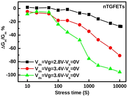
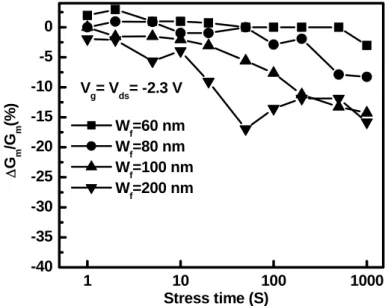
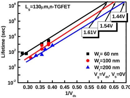
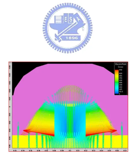
(19) Fig.3-16 Drain-induced-barrier-lowering of MSB and CN TGFETs with different fin thicknesses as Lg =130nm and 49nm. Fig.3-17 Transfer characteristics of the MSB TGFET with Lg=65nm Wf=60nm, and TSi=40nm measured at temperatures from 100K to 500K. Fig.3-18 Arrhenius plots of Ioff at Vgs-Vth=0.75V and Vds=-1V of the MSB and CN TGFETs with Lg=6 nm Wf =60nm, and TSi=40nm.. Chapter 4 Fig.4-1. Schematic diagram of NBT stress conditions for p-TGFETs. The source, drain, and back-gate are connected to ground. And then, the stress voltage is applied to the gate electrode (Vg).. Fig.4-2. (a) Ion degradation, (b) Vth shift and (c) Gm variations of p-TGFETs (Lg=65nm, Wf=40nm, TSi=40nm) for stress voltages of Vg=Vth, Vg=1/2Vds, and Vg=Vds=-2.2V.. Fig.4-3. Time-dependence power-law plot of ΔIon/Ion vs. stress time for p-TGFETs with Lg=65nm, Wf=40nm, and TSi=40nm stressed at Vg=Vth,, 1/2Vds, and Vds, respectively.. Fig.4-4. (a) Ion degradation, (b) Vth shift and (c) Gm variations of n-TGFETs (Lg=130nm, Wf=80nm, TSi=40nm) for stress conditions of Vg=Vth and Vg=Vds=-3.2V.. Fig.4-5. Gm degradation of (a) n- and (b) p-TGFETs with Lg=130nm, Wf=60nm, and TSi=40nm stressed at Vg=Vds with biased at 2.8, 3.4, and 3.6V.. Fig.4-6. (a) Gm and (b) Ion degradation of p-TGFETs with Lg=65nm, TSi=40nm, and different Wf (60, 80, 100, and 200nm) were stressed at Vds=Vg=-2.3V.. Fig.4-7. (a) Lifetime prediction of p-TGFETs with two Lg (130 and 49nm) and xvii.
(20) several Wf (60, 100, 200 nm). (b) Operation voltage at 10-yr DC lifetime vs. different Wf. Fig.4-8. N-TGFETs lifetime prediction with different Wf stressed at (a) Vg=Vds and (b) Vg=Vth.. Fig.4-9. (a) Potential contour and (b) electrical field direction of Si fin with Wf=200nm and TSi=40nm stressed at Vds=Vg=2.3V.. Fig.4-10 (a) Potential contour and (b) electrical field direction of Si fin with Wf=40nm and TSi=40nm stressed at Vds=Vg=2.3V. Fig.4-11 (a) Cross-sectional schematic view of Si fin with Wf=TSi=40nm. The AA’ and BB’cut-line is at 5nm and 30nm under the top interface between SiO2/Si. The electric field strength along (b) AA’ and (c) BB’ cut-lines for Si fin with different Wf increasing from 20 to 200nm. Fig.4-12 TEM planar views of Si fin with (a) Wf=200, Lg=49nm and (b) Wf=40nm, Lg=49nm. Fig.4-13 Schematic planar views of Si fin with (a) Wf=200, Lg=49nm and (b) Wf=40nm, Lg=49nm. Fig.4-14 Shift of Vth for p-TGFETs with Lg=130nm, Wf=40nm, and TSi=40nm at NBTI stress conditions with Vg=Vth-3.2, Vth-3.5, Vth-4, and Vth-4.5V, respectively. Fig.4-15 (a) Ion, (b) Gm and (c) Vth degradation of p-TGFETs with Lg=130 nm, and TSi=40nm and several Wf(60, 80, and 100nm) stressed at Vg=-4.5V and Vd=Vs=0V.. Chapter 5 Fig.5-1. Schematic views of HCI measurement for TGFETs with a fixed Vds, Vg, xviii.
(21) and various Vb. Fig.5-2. (a) Schematic cross-sectional view of TGFETs stressed with front-gate (Vg) and back-gate bias (Vb). (b)TEM cross-sectional view of TGFETs with Lg=130nm, Wf=40nm, and TSi=40nm. The front gate oxide and buried oxide thickness is 4nm and 150nm, respectively. The excess gate length (DEXT) is 8nm.. Fig.5-3. Transfer characteristics of n-TGFETs with Lg=10μm, Wf=10μm, and TSi=40nm and various Vb increases from -20V to 20V (step=2V).. Fig.5-4. (a) S.S., (b) Vth and (c) Gm variations of n-TGFETs with Lg=10mm, Wf=10mm, and TSi=40nm different Vb (from -21 to 21 V, step=1V).. Fig.5-5. Transfer characteristics of n-TGFETs with Lg=130nm, Wf=40nm, and TSi=40nm and various Vb increases from -21V to 21V (step=1V).. Fig.5-6. (a) S.S., (b) Vth, and (c) Gm variations of n-TGFETs with Lg=130nm, TSi=40nm, various Wf (60, 80, 200, 500, and 1000 nm) and different Vb (from -21 to 21 V, step=1V). The inset figure of Fig.5-6(b) shows the Vth variations of devices with Wf=80nm and slope "A" separately.. Fig.5-7. Gm peak ratio between point "C" and "B" in Fig.5-6(c).. Fig.5-8. Transfer characteristics of back channel n-TGFETs devices with Lg=130nm, Wf=60nm, TSi=40nm and buried oxide thickness=150nm.. Fig.5-9. Transfer characteristics of back channel n-TGFETs devices with Lg=130nm, Wf=60nm, TSi=40nm and buried oxide thickness=150nm.. Fig.5-10 The cross-sectional electric field simulation with Vds=Vg=3.2V, and Vb=-10V for devices with a fixed Lg (130nm) and TSi (40nm) and various Wf and DEXT (a) Wf=40nm, DEXT=0nm, (b) Wf=40nm, DEXT=8nm, (c) Wf=40nm, DEXT=16nm, and (d) Wf=200nm, DEXT=16nm.. xix.
(22) Fig.5-11 (a) Gm and (b) Vth variations of n-TGFET with Lg=130nm, Wf=100nm, and TSi=40nm after stressed at Vds=Vg=3.2V and Vb=0V or floating. Fig.5-12 Schematic photos of (a) process cycle for HCI measurement and (b) HCI stress conditions of devices. Fig.5-13 (a) Vth, (b) Gm and (c) Ion variations of n-TGFET with Lg=130nm, Wf=100nm, and TSi=40nm after stressed at Vds=Vg=3.2V and Vb=-10 V (N) or 5V (P). Fig.5-14 (a) Gm and (b) Vth degradation of n-TGFET devices with Lg=130nm, Wf=80nm, and TSi=40nm after stressed at Vds=Vg=3.2V and different Vb (from -30 to 5 V, step=5V). Fig.5-15 Schematic views of virtual back-gate effect after HCI stressed with negative back-gate bias. Fig.5-16 (a) Forward mode and (b) reverse mode transfer characteristics of back channel n-TGFETs devices (Lg=130nm, Wf=100nm, TSi=40nm and BOX=150nm) before/after stressed with Vds=Vg=3.2V, Vb=-20V for 3000second. Fig.5-17 (a) Gm variations vs. stress time and (b) the ratio between the rebounded point and the initial values of n-TGFETs with a fixed Lg=130nm and TSi=40nm and various Wf (40, 60, 100, 200nm) stressed with Vds=Vg=3.2V and Vb=-20V.. Chapter 6 Fig.6-1. Key fabrication process steps of n-and p-channel FUSI-ITS-gate MSB FD-SOI devices.. Fig.6-2. Key fabrication process steps of n-and p-channel polycide-gate MSB xx.
(23) FD-SOI devices. Fig.6-3. Schematic figures of (a) FUSI-ITS-gate, (b) polycide-gate MOS capacitance structures.. Fig.6-4. C-V Curve of Ni-Polycide and FUSI-ITS gated MOS-capacitances. For FUSI-ITS gate, the VFB values decreases with the increasing of P31+ dopants from w/o implant and 1x10¹⁵.. Fig.6-5. Extracted work function (Φm) of the NiSi and polycide gate on SiO2.. Fig.6-6. SIMS in-depth profiles of the FUSI-ITS-gate MOS-capacitances implanted with (a) P31+ and (b) BF2+ of 1x1015cm-2.. Fig.6-7. XRD profiles of FUSI-ITS samples after silicidation, P31+ implantation, and annealing at 600oC for 30 min., respectively. The film structures after silicidation and annealing are almost the same and without any influences of impurity species.. Fig.6-8. Cross-sectional TEM figure of FUSI-ITS-gate MOS-capacitances. The perfect Ni-silicide/gate oxide interface was showed; while, no residual poly-Si islands was found.. Fig.6-9. Cross-sectional TEM figure of FUSI-ITS-gate MSB FD-SOI devices. The S/D/G electrode could be fully-silicided at the same time.. Fig.6-10 Transfer characteristics of n-and p-channel FUSI-ITS-gate MSB FD-SOI devices. Fig.6-11 Transfer characteristics of n- and p-channel polycide-gate MSB FD-SOI devices. Fig.6-12 Transfer characteristics of FUSI Schottky-barrier FD-SOI device without any implantation process. Fig.6-13 Output curves of n-and p-channel FUSI-ITS-MSB FD-SOI devices with. xxi.
(24) Lg/W=1μm/1μm. Fig.6-14 Comparisons of driving currents for n-channel FUSI-ITS and polycide MSB FD-SOI devices with Lg/W=1μm/1μm.. Chapter 7 Fig.7-1. Key fabrication steps OF the proposed FSD TFTs.. Fig.7-2. Cross-sectional transmission electron microscopy (TEM) image of the proposed FSD TFTs activated at 600ºC for 30 sec in a N2 ambient. (b) The EDX analysis data of point “A”.(c) The EDX analysis data of point “B”.. Fig.7-3. Schematic cross-sectional drawings of (a) CN TFTs and (b) SB TFTs.. Fig.7-4. Typical transfer characteristics of FSD and CN (a) n- and (b) p-TFTs after NH3 plasma treatment.. Fig.7-5. Typical transfer characteristics of SB n- and p-TFTs after NH3 plasma treatment.. Fig.7-6. (a)Typical transfer characteristics of FSD TFTs implanted P31+ with 5x1012cm-2. (b)Transfer and (c) output characteristics of FSDTFTs implanted P31+ with 5x1013cm-2.. Fig.7-7. Comparison of output characteristics between a FSD and CN n-TFT with W/L=1μm/4μm.. Fig.7-8. Parasitic resistance (Rp) of (a) FSD and (b) CN n-TFTs in the linear region, is also extracted by plotting the width-normalized on-state resistance (Ron) versus channel length (L).. Fig.7-9. Transfer characteristics of FSD (a) p- and (b) n-TFTs activated at. xxii.
(25) different temperatures (600, 650, 700, and 750 0C). Fig.7-10 Sheet resistance (Rsh) comparison between the silicide at S/D and gate electrode activated at different temperature (550, 600, 650, 700, 750 0C for 30seconds). Fig.7-11 Effective trap-state density (Nt) of source/drain and gate electrode with different activation temperatures (550, 600, 650, 700, and 750 0C for 30seconds). Fig.7-12 Jg-Vg leakage current plots of. FSD TFTs activated at different. temperatures (600, 650, 700, and 750 0C). Fig.7-13 SEM images of Ni silicide on the poly-Si/oxide substrate activated at (a) 600oC, (b) 650oC, (c) 700oC, and (d) 750oC for 30sec. Fig.7-14 X-ray diffraction (XRD) spectra of the silicide on the poly-Si gate electrode after 600oC for 30s, 600oC for 120s, and 750oC for 30s annealing conditions. Fig.7-15 (a) Cross-sectional TEM figure of FSD TFTs after 750oC for 30seconds activation. (b) and (c) are the EDX analysis data of point “A” and “B” in (a). Fig.7-16 (a)Cross-sectional TEM figure of FSD TFTs after 750oC for 30seconds activation. (b) and (c) are the EDX analysis data of point “A” and “B” in (a). Fig.7-17 Transfer characteristics of FSD (a) p- and (b) n-TFTs with different RTA activation time (30, 90, 150 seconds) at 600ºC, respectively. Fig.7-18 Extraction of RSh of S/D/G electrode after 600 ºC for 30, 90, and 150 sec annealing. Fig.7-19 Vth roll-off characteristics of FSD and CN n- and p-TFTs with W=3μm.. xxiii.
(26) Fig.7-20 Driving current degradation of FSD and CN n-TFTs with the stress gate voltage. The stress conditions are at Vds=20V and various Vg from 6 to 26V with step is 2V. Fig.7-21 Forward mode transfer characteristics of (a) FSD and (b) CN n-TFTs before and after hot-carrier application. The stressing conditions was Vg=6V and Vds=20V for a stress time of 3600s. The size of TFT W/L=5μm/5μm. Fig.7-22 Reverse mode transfer characteristics of (a) FSD and (b) CN -TFTs before and after hot-carrier application. The stressing conditions was Vg=6V and Vds=20V for a stress time of 3600s. The size of TFT W/L=5μm/5μm. Fig.7-23 Time dependence of forward mode maximum transconductance (ΔGm/Gm) degradation of FSD and CN n-TFTs after various hot-carrier stressing time. The stressing conditions was Vg=6V and Vds=20V for a stress time of 3600s. The size of TFTs W/L=5μm/5μm. Fig.7-24 Forward mode transfer characteristics of (a) FSD and (b) CN nTFTs before and after self-heating application. The stressing conditions was Vg=20V and Vds=20V for a stress time of 3600s. The size of TFT W/L=5μm/5μm. Fig.7-25 Reverse mode transfer characteristics of (a) FSD and (b) CN n-TFTs before and after self-heating application. The stressing conditions was Vg=20V and Vds=20V for a stress time of 3600s. The size of TFT W/L=5μm/5μm.. Chapter 8 xxiv.
(27) Fig.8-1. Key fabrication process of HfO2 poly-Si n-TFTs.. Fig.8-2. (a) Schematic and (b) TEM views of HfO2 poly-Si n-TFTs. The physical thickness of HfO2 is equal to 27.7nm, and that of the bottom interfacial layer is about 2nm.. Fig.8-3. Measurement data of high-frequency (100KHz) capacitances of HfO2 and SiO2 capacitance.. Fig.8-4. (a) Transfer, (b) output and (c) Ig-Vg characteristics of HfO2 n-TFTs (Lg=1μm and Wg=0.1μm) with different NH3 passivation time with 2, 4, and 6 hrs.. Fig.8-5. (a) Output and (b) transfer characteristics of HfO2 and SiO2 n-TFTs with Lg=1mm and Wg=0.1mm after a 30min NH3 plasma treatment.. Fig.8-6. The. Vth. roll-off. phenomena. of. n-TFTs. (Wg=1μm). with. HfO2. (Tphys.=27.7nm) and SiO2 (Tphys.=25nm and 45nm). Fig.8-7. Transfer characteristics of HfO2 n-TFTs with a fixed Lg=1μm and three different channel width (Wg) of 1μm, 0.3μm to 0.1μm was measured at Vds=0.1V.. Fig.8-8. (a) Ion and Ioff, (b) Gm and S.S. and (c) Vth variations of HfO2 n-TFTs with a fixed Lg=1μm and various channel width.. xxv.
(28) xxvi.
(29) Chapter1 Introduction 1-1 The Evolution of CMOS In 1963, the first CMOS circuit was invented by Frank Wanlass [1-1]. Then, some twenty-five years latter, it became the predominant technology in very large scale integrated circuits. To approach the benefits such as high performance, high operation speed, high device density, low power consumption, and low manufacturing costs, the dimension downsizing of CMOS becomes the principled trend for the last few decades. This trend basically traced back to the Moore’s Law, the observation by Gordon Moore in 1965 , which was often stated as the doubling of transistor performance and quadrupling of the number of devices on a chip every three years [1-2]. Following the Moore’s law, by 1992, the Semiconductor Industry Association (SIA) has been first published the technology roadmap for semiconductors. This roadmap represents a consensus outlook of industry trends, taking history as a guide. In 2003, the roadmap pointed out that the technology will step to 45 nm node beyond 2010, as shown in Fig.1-1 [1-3]. It is well known that the major challenges of extending CMOS beyond 45nm node are the suppression of poor short-channel effects (SCE) attributed to the insufficient gate-controllability and the abnormal large leakage current due to the ultra-thin gate dielectric. Therefore, to alleviate these issues, two avenues have been suggested: new non-classical structures and new materials. Non-classical CMOS structure includes transport-enhancement FETs,. 1.
(30) ultra-thin-body (UTB) SOI FETs, and 3-dimensional structure FETs (3D FETs) such as. double-gate. FETs. and. multi-gate. FETs. (MGFETs). [1-3].. In. the. transport-enhancement FETs, the carrier mobility could be enhanced by the mechanical strain in the channel layer or by the judicious choice of crystal orientation and current transport direction [1-4]. However, material defects, junction leakage current, process compatibility, and operating temperature are still issues. For the UTB SOI FETs, the ultra-thin lightly-doped body could effectively reduce the leakage current while enhance the driving capability. Nevertheless, the requirement of low-defect ultra-thin body and controllability of threshold voltage (Vth) are still problems [1-5]. Quantum confinement also limits the improvement in performance. Therefore, 3D FETs including double-gate FETs (such as FinFETs) and MGFETs (such as tri-gate FETs) attracted many attentions in these years [1-6]-[1-7]. Especially, MGFET is the plausible solution beyond the 45nm technology node.. 1-2 Why Multi-Gate FETs? Why the multi-gate FET (MGFETs) is the most attractive candidate structure beyond the 45 nm technology node ? Taking the tri-gate FET (TGFET) as an example, although the fully-depleted SOI transistors have the advantages resided in the simplicity of the process (close to bulk planar process), the compactness of the layout (same as for bulk planar), and competitive with a similarly-scaled, aggressive bulk CMOS technology at the same technology node. Nevertheless, to scale the dimension of the active silicon channel region of the fully-depleted (FD) SOI transistors is still the major challenge [1-8]. In the case of single-gate FDSOI devices, the silicon body thickness (TSi) needs to be about a third of the electrical gate length in order to maintain full substrate depletion under gate control [1-9]. Moreover, the 2.
(31) threshold voltage (Vth) could also be affected by the Si thickness variation [1-10]. Scaling this device to 30 nm gate length dimensions, for example, requires a 3σthickness uniformity of 1 nm on a silicon film thickness of 10 nm, which is presently hard to achieve. Double-gate FET is one of the 3D FET structures, the typical one is the FinFET, in which the current flows horizontally (parallel to the plane of the substrate) between the source and drain along the two opposite vertical channel surfaces. The width of the vertical silicon fin should be narrow (smaller than the channel length) to provide adequate control of the SCE. A lithographically defined gate straddles the fin, forming self-aligned, electrically connected gate electrodes along the sidewalls of the fin. The principal advantage with this structure is the planar bulk-like layout and process compatibility. The major challenge is the width of the thin fins should be thicker than a half of the gate length. To further relax the gate length constrain of FinFETs, TGFETs were simulated and fabricated [1-11]-[1-13]. They have not only been reported to show fully depleted behavior at thickness dimension greater than that of the single-gate FD SOI and FinFET, but also relaxes the acquirement of high Si fin etching process of FinFETs and of the active layer thickness uniformity of single-gate FD SOI devices. Therefore, the TGFET has emerged as a very promising candidate among single-, double-, and multi-gate ones in the end of ITRS roadmap. The comparison among the 3D FETs are summarized in Table.1-1 [1-3].. 1-3 Modified-Schottky-Barrier (MSB) TGFETs Although the TGFET has been considered as a candidate structure beyond 3.
(32) 45nm technology node, some technical problems such as shallow source/drain (S/D) junction formation, the source/drain and gate (S/D/G) electrode parasitic resistance (Rp) reduction, and the process temperature compatibility between the high-dielectric constant dielectric (high-κ) and S/D activation still exist. In conventional bulk CMOS, to suppress the large Rp at S/D electrode, many silicide technologies have been suggested in the past twenty years. However, the silicidation of S/D region is a great-skill work. Improper silicidation scheme may result in unacceptable high leakage current due to the numerous consumption of the heavily doped regions [1-15]. The resultant I-V characteristics and contact resistance may be degraded. Furthermore, it is very hard to fabricate sub-0.1μm junctions by means of conventional high temperature activation process [1-16]. On the other hand, Schottky barrier source/drain structure has been suggested in 1994 by J. R. Tucker et al., [J. R. Tucker, APL, p.618, 1994], and have been demonstrated to release the acquirement of Rp and preserve the short extension length [1-14]. Nevertheless, not only the abnormally high contact resistance attributed to the Schottky-barrier (SB) junction at source-side can degrade the driving capability, but the small SB at drain-side also results in high off-state leakage current [1-17]. Therefore, to solve those problems, in this thesis, the implant-to-silicide (ITS) technique is suggested to fabricate nano-scale TGFETs. This ITS technique has been proposed as a promising solution to form sub-0.1 shallow junctions at low temperature and has been investigated widely in the 90’ decade [1-18]-[1-21]. It uses a silicide film to act as an ion-implantation damage basin and thus the process temperature can be greatly reduced. The silicide film also acts as an energy barrier for the implanted ions and thus shallow junctions can be obtained using the implanted silicide film as solid diffusion source. This merit is especially important and useful for 4.
(33) p+n junctions because boron is a very light element and is a fast diffuser in silicon.. 1-4 ITS Technique on Fully-Silicide Gate Electrodes To suppress the SCE while control the Vth well, except the device structure modification such as TGFETs and Schottky-barrier S/D, the gate controllability enhancement by metal gate electrode and high-κ gate dielectric are also possible solutions [1-22]. Recently, fully silicided poly-Si (FUSI) gate has been proposed to replace the conventional doped poly-Si gate to solve the gate depletion problem while release the thermal stability issue of high-κ gate dielectric [1-23]. From the characteristics perspective, Ni-silicide FUSI gate has several advantages such as low-silicidation temperature, low sheet resistance, low stress and an intrinsically mid-gap workfunction (WF) [1-24]. Recently, the ITS process has been demonstrated as an effective method to adjust the work function of Ni-FUSI gate while removing the NiSi phase and crystal orientation influences [1-25]-[1-26]. In order to preserve the advantages of Ni-FUSI gate while simplify the process integration and stabilize the work function, integrate FUSI gate and MSB S/D structure by ITS process on FD-SOI devices should be an ideal approach. Consequently, not only the NiSi gate work function could be adjusted by the dopant piled-up at the interface between the NiSi/gate dielectric, the low S/D parasitic resistance could also be preserved. Moreover, the process issues such as implantation damage of gate dielectric, the S/D/G silicidation depth, and the thermal budget consideration are all effectively improved.. 5.
(34) 1-5 ITS Technique on Poly-Si TFTs Besides the CMOS, poly-Si thin-film transistor is another important and popular semiconductor device to be applied to the active-matrix-driven flat panel display (FPD). To enhance the switching characteristics while reduce the amount of external interconnections, pixel-driving circuits monolithically integrated on the display panel substrate to form the system-on-panel is the future trend [1-27]. In order to integrate peripheral driving circuits on the same glass substrate, a low-temperature process (~600°C) without compromising device performance should be developed. The conventional long post-ion-implantation annealing used to activate dopants and remove implantation damages is carried out in a furnace system at around 600°C for 12-24 hours after the source/drain implantation [1-28]. This is an unacceptable thermal budget. On the other hand, the use of a thinner active layer to obtain higher driving current, lower off-state leakage current, and superior short channel characteristics has been reported [1-29]-[1-30]. Because of the temperature restriction and the thin active layer structure, the high Rp from thin source/drain (S/D) regions would degrade device performance such as driving capability and effective field effect mobility (μFE). To reduce the S/D Rp of poly-Si TFTs while preserve the benefit of thin-active layer structure and restrict the process beyond 600oC, also it is possible to apply the NiSi and ITS technique to form S/D electrode to the poly-Si TFTs and named fully-silicided S/D TFTs (FSD TFTs). Similar to the MSB TFGET, this novel FSD TFT (FSD TFT) structure has the fully-silicided source/drain and ultra-short source/drain extension (SDE) at the interface of silicide and inverted channel by the implant-to-silicide (ITS) technique. Forming a fully silicided source/drain by the low. 6.
(35) temperature self-aligned salicide technique, the Rp of FSD TFTs can be decreased dramatically. Adding an extension doping in the silicon by the ITS technique at about 600oC not only drastically improves the contact resistance at the Ni-silicide/poly-Si junction but also abbreviates the source/drain extension length and avoids the silicide spiking effect. To further enhance the switching characteristics of poly-Si TFTs, similar to the CMOS process, a thin and high-quality gate dielectric layer is required for future poly-Si TFTs. A major problem in gate dielectric layer on the poly-Si TFTs is local breakdown due to the rough silicon surface [1-31]. Because of this problem, gate dielectric layer on the poly-Si TFTs has to be deposited thicker than necessary to overcome the surface roughness, which reduces TFT drivability. For TFTs with a sub-micron scale, a thick gate dielectric could also degrade the other electrical characteristics. Recently, hafnium dioxide (HfO2) becomes a candidate of future high-κ gate dielectric material in MOSFET due to its high κ value (15~25), wide bandgap, and acceptable band alignment [1-32]-[1-33]. Therefore, we also use HfO2 as gate dielectric layer of poly-Si TFTs for the first time.. 1-6 Thesis Organization In the first chapter of this dissertation, we briefly review the revolution of the novel nano-CMOS and the shortcomings of current poly-Si TFTs technology. For CMOS, the advantages and necessity of integrating TGFETs structure, NiSi material, and ITS technique are also stated. For poly-Si TFTs, we also suggested that the fully silicided S/D and HfO2 gate dielectric could effectively improved the device characteristics. To implement and verify these concept, in chapter 2, a thorough study on 7.
(36) the characteristics of NiSi line including the sheet resistance and lateral silicidation rate are performed. The thermal stability of NiSi on four different substrates, amorphous-Si, poly-crystalline-Si, crystalline-Si, and silicon dioxide, are also demonstrated for the first time. In chapter 3, the fabrication process and electrical characteristics of the proposed novel TGFETs featuring with modified-Schottky-barrier (MSB) S/D structure are demonstrated. The MSB S/D process not only lowers the S/D process temperature, but also reduces the Rp of S/D/G electrodes. Moreover, because of the ultra-low activation temperature, the ultra-shallow S/D extension length could be controlled easily and the proposed devices have better electrical characteristics than that with conventional implantation and activation technology. In chapter 4, the reliability characteristics of n- and p-channel MSB TGFETs are investigated in detail. As devices scale down, the immunity of hot-carrier stress for n-channel and negative-bias-temperature stress for p-channel devices became significantly. However, for the TGFETs with ultra-nano fin width and multiple gate electrodes, the degradation phenomenon and mechanisms are very different from those of the conventional CMOS. In the chapter 4, the relationship among the reliabilities, fin width, and silicide front-edge roughness will be discussed. In chapter 5, we extend the reliability studies of n-channel TGFETs to the back gate bias (Vb) effect. Because of the poor qualities of buried oxide in the SIMOX wafer, the Vb effect not only affects the basic I-V characteristics of SOI devices, the reliability characteristics are also influenced seriously. In this chapter5, we demonstrate that for the TGFET with narrow fin width, the effects of Vb effect on I-V characteristics and reliabilities could be relaxed by the small bottom interface area between Si fin/buried oxide and the electrical field shielding effect by the side-gate. 8.
(37) extension length. In chapter 6, the fabrication process and electrical characteristics of n-and p-channel FD SOI devices featuring with the fully-silicide gate electrode (FUSI) and MSB S/D electrode using the ITS technique are demonstrated for the first time. It is confirmed that the FUSI gate can eliminate the poly-depletion effect. Moreover, using the ITS technique to the FUSI gate not only relax the thermal stability issues of high-k gate dielectric, but also adjust the work function effectively. In chapter 7, we report the process and characteristics of FSD poly-Si TFTs. The same advantage of higher driving current due to the low S/D resistance as the conventional salicide TFTs is obtained. The effects of process conditions on electrical characteristics of the proposed devices are discussed thoroughly. Besides, the hot-carrier characteristics of the proposed FSD poly-Si TFTs are also addressed. In chapter 8, we integrate poly-Si TFTs with HfO2 gate dielectric. The characteristics of the HfO2 TFTs are described and compared to the conventional SiO2 TFTs with the same physical gate dielectric thickness. The recorded effective gate oxide thickness of 7.314nm for poly-Si TFT is demonstrated. Both the NH3 plasma treatment and narrow width effects numerously improve the characteristics of the HfO2 TFTs. Finally, in the chapter 9, we summarize important conclusions achieved in this dissertation. Some future works worthy to study continuously are recommended.. 9.
(38) References [1-1]. M. J. Riezenman, “Wanlass’s CMOS circuit,” in IEEE Spectrum, vol. 8, pp.44, 1991.. [1-2]. Gordon E. Moore, “Cramming more components onto integrated circuits,” in Electronics, vol.38, pp.8, 1965.. [1-3]. International Technoloqy Roadmap for Semiconductors(ITRS), 2003 edition, see http://public.itrs.net/Files/2003ITRS/Home2003.htm.. [1-4]. B. H. Lee, A. Mocute, S. Bedell, H. Chen, D. Sadana, K. Rim, P. O’Neil, R. Mo, K. Chen, C. Cabral, C. Lavoie, D. Mocuta, A. Chakravarti, R. M. Mitchell, J. Mezzapelle, F. Jamin, M. Sendelbach, H. Kermel, M. Gribelyuk, A. Domeniucci, K. A. Jenkins, S. Narasimha, S. H. Ku, M. Ieong, I. Y. Yang, E. Leobandung, P. Agnello, W. Haensch, and J. Welser, “Performance enhancement on sub-70 strained silicon SOI MOSFETs on ultra-thin thermally mixed strained silicon/SiGE on insulator (TM-SGOI) substrate with raised S/D,” in IEEE IEDM Tech. Dig., 2002, pp. 946-948.. [1-5]. B. Doris, M. Ieong, T. Kanarsky, Y. Zhang, R. A. Roy, O. Dokumaci, Z. Ren, E.E. Jamin, L. Shi, W. Natzle, H. J. Huang, J. Mezzapelle, A. Mocuta, S. Womack, M. Gribelyuk, E. C. Jones, R. J. Miller, H.-S. P. Wong, and W. Haensch, “Extreme scaling with ultra-thin Si channel MOSFETs,” in IEEE IEDM Tech. Dig., 2002, pp. 267-270.. [1-6]. B. Yu, L. Chang, S. Ahmed, H. Wang, S. Bell, C. Y. Yang, C. Tabery, C. Ho, Q. Xiang, T.-J. King, J. Boker, C. Hu, M.-R. Lin, D. Kyser, “FinFET scaling to 10nm gate length,” in IEEE IEDM Tech. Dig., 2002, pp. 251-254.. [1-7]. Y. K. Choi, L. Chang, P. Ranade, J. S. Lee, D. Ha, S. Balasubramanian, A. Aarwal, M. Ameen, T.-J. King, and J. Bokrt, “ FinFET process refinements for 10.
(39) improved mobility and gate work function engineering,” in IEEE IEDM Tech. Dig., 2002, pp. 259-262. [1-8]. H.-S. P. Wong, D. J. Frank, and P. M. Solomon, “Device design considerations for double-gate, ground-plane, and single-gated ultra-thin SOI MOSFET’s at the 25 nm channel length generation,” in IEDM Tech. Dig., 1998, pp. 407–410.. [1-9]. R. H. Yuan, A. Ourmazd, and K. Lee, “Scaling the Si MOSFET: from bulk to SOI to bulk,” IEEE Trans. Electron Devices, vol. 39, pp.1704–1710, 1993.. [1-10] J. Chen, R. Solomon, T.-Y. Chan, P. K. Ko, C. Hu, “Threshold voltage and C-V characteristics of SOI MOSFET’s related to Si film thickness variation on SIMOX wafers,” in IEEE Trans. Elec. Dev., vol. 39, pp.2346-2353, 1992. [1-11] B. S. Doyle, S. Datta, M. Doczy, S. Hareland, B. Jin, J. Kavalieros, T. Linton, A. Murthy, R. Rios, R. Chau, “High performance fully-depleted tri-gate CMOS technique,” in IEEE Elec. Dev. Lett., vol.24, pp.263-265, 2003. [1-12] A. Breed, K. P. Roenker, “Dual-gate (FinFET) and tri-gate MOSFETs: simulation and design,” in Symp. Semi. Dev. Res., 2003, pp150-151. [1-13] S. E. Thompson, R. S. Chau, T. Ghani, K. Mistry, S. Tyagi, M. T. Bohr, “In search of ‘Forever,’ continued transistor scaling one new material at a time,” in IEEE Trans. Semi. Manufac., vol. 18, 2005, pp. 26-26. [1-14] M. Nishisaka, Y. Ochiai, and T. Aasano, “Pt-silicide source and drain SOI-MOSFET operating in Bi-channel modes,” in Conf. Dev. Research. Dig., 1998, pp.74-75. [1-15] S. P. Murarka, Silicides for VLSI application, New Work: Academic, 1983, p.130. [1-16] T. Hoffmann, G. Doornbos, I. Ferain, N. Collaert, P. Zimmerman, M. Goodwin,. 11.
(40) R. Rooyackers, K. G. Anil, Y. Yim, M. Jurczak, S. Biesemans, “GIDL(gate-induced drain leakage) and parasitic Schottky barrier leakage elimination in aggressively scaled HfO2/TiN FinFET devices,” in IEEE IEDM Dig., 2005, pp.743-746. [1-17] J. P. Snyder, C. R. Helms, and Y. Nishi, “Experimental investigation of a PtSi source and drain field emission transistor,” in App. Phys. Lett., vol. 67, pp.774-776, 1995. [1-18] J. Lebowitz, R. Liu, S. J. Hilenius, W. T. Lynch, “IIIB-3 modified Schottky behavior in shallow p+n junctions formed by outdiffusion from Cobalt silicide,” in in IEEE Trans. Elec. Dev., vol. 34, pp.2366-2366, 1987. [1-19] B. Y. Tsui, and M. C. Chen, “A novel process for high-performance Schottky barrier PMOS,” J. Electrochem. Soc., vol. 136, pp.1456, 1989. [1-20] F. La Via, C. Spinella, and E. Rimini, “Arsenic and boron diffusion in silicon from implanted cobalt silicide layers,” in Semicond. Sci. Technol., vol. 10, pp.1362-1367, 1995. [1-21] Q. F. Wang, C. M. Osburn, and C. A. Canovai, “Ultra-shallow junction formation using silicide as a diffusion source and low thermal budget,” in IEEE Trans. Elec. Dev., vol.39, pp.2486-2496, 1992. [1-22] D. A. Buchanan, “Scaling the gate dielectric: materials, integration, and reliability,” in IBM. J. Res. & Dev., vol.43, pp.245-264, 1999. [1-23] W. P. Maszara, Z. Krivokapic, Z. King, J.-S. King, M.-R. Lin, “Transistors with dual work function metal gates by single full silicidation (FUSI) of polysilicon gates,” in IEEE IEDM Dig., 2002, pp.367-370. [1-24] K. Sano, M. Hino, N. Ooishi, and K. Shibahara, “Workfunction tuning using various impurities for fully silicided NiSi gate,” in Int. Conf. Solid State. 12.
(41) Device and Materials, 2004, pp.456-457. [1-25] Y. Tsuchiya, M. Yoshiki, M. Koyama, A. Kinoshita, J. Koga, “Physical mechanism of work function modulation due to impurity pileup at Ni-FUSI/SiO(N) interface,” in IEDM Tech. Dig., 2005, pp.637-640. [1-26] C. F. Huang and B. Y. Tsui, “Analysis of NiSi fully-silicided gate on SiO2 and HfO2 for CMOS application,” in Int. Conf. Solid State Device and Materials., 2005, pp.506-507. [1-27] T. Nishibe, “Low-temperture poly-Si poly-Si TFT by excimer laser annealing,” in Mat. Res. Soc. Symp., vol. 581E, pp. D.6.1.1-D.6.1.4, 2001. [1-28] H. W. Zen, T. C. Chang, P. S. Shih, D. Z. Pong, P. Y. Kuo, T. Y. Huang, C. Y. Chang, and P. T. Liu, “A study of parasitic resistance effects in thin-channel polycrystalline silicon TFTs with Tungsten-clad source/drain,” in IEEE Electron Device Lett., vol. 24, pp.509-511, 2000. [1-29] A. Kumar K. P., J. K. O. Sin, C. T. Nguyen, and P. K. Ko, “Kink-free polycrystalline silicon double-gate elevated-channel thin-film transistors,” in IEEE Trans. Electron Devices, vol.45, pp.2514-2520, 1998. [1-30] S. Zhong, R. Han, and M. J. Chan, “A novel self-aligned bottom gate poly-Si TFT with in-situ LDD,” in J. Electrochem. Soc., vol.136, pp.1456-1459, 1989. [1-31] J. K. Lee, J. B. Choi, S. M. Seo, C. W. Han, and H. S. Soh, “The application of tetraethooxysilane (TEOS) oxide to a-Si:H TFT’s as the gate insulator,” in SID Dig., vol.29, 1998, pp.454-458. [1-32] C. Hobbs, H. Tseng, K. Reid, B. Taylor, L. Hebert, R. Garcia, R. Hegde, J. Grant, D. Gilmer, A. Franke, V. Dhandapani, M. Azrak, L. Prabhu, R. Rai, S. Bagchi, J. Conner, S. Backer, F. Dumbuya, B. Nguyen, and P. Tobin, “80 nm poly-Si gate CMOS with HfO2 gate dielectric,” in Int. Electron Devices. 13.
(42) Meeting Tech. Dig., 2001, pp. 651-654. [1-33] Y. Kim, C. Lim, C. D. Young, K. Mathews, J. Barnett, B. Foran, A. Agarwal, G. A. Brown, G. Bersuker, P. Zeitzoff, M. Gardner, R. W. Murto, L. Larson, C. Metzner, S. Kher, H. R. Huff, “Conventional poly-Si gate MOS-Transistors with a novel, ultra-thin Hf-oxide layer,” in IEEE Symp. VLSI Tech. Dig., 2003, pp. 167-168.. 14.
(43) Table1-1 Comparisons of non-classical CMOS.. Device types Advantages. Transportenhanced FETs High mobility. UTB-SOI FET 1.Improved. FinFETs 1. Higher drive. 2.subthreshold slope No floating body. current 2. Improved subthreshold slope. TGFETs 1.Higher drive current 2.2x thicker fin allowed. 3. Improved short channel effect. Particular Strength. High mobility. 1.Low diode leakage. Relatively easy. Thicker Si body. without change in. 2. Low junction capacitance. process integration. possible. device. 3. No significant change in. 1. Fin thickness less. 1.Limited device. architecture. Potential Weakness. 1. Material defects & diode leakage 2. Process compatibility &. design with respect to bulk. 1.very thin silicon required with low defect density 2. Vth adjustment difficult 3. Selective epi required for elevated S/D. than the gate length. width 2.Corner effect. 2. Fin shape & aspect ratio. thermal budget 3.Operating temperature. Scaling Issues. Bandgap usually. Control of Si film thickness. smaller than Si. Sub-lithographic fin. Sub-lithographic. thickness required. fin thickness required. Impact on Ion/Ioff*@. Impact on CV/I*. @. Improved by. Improved by 15–20%. 20–30%. Lowered by. Lowered by 10–15%. 15–20%. Improved by. Improved by. 20–30%. 20–30%. Lowered by. Lowered by. 15–20%. 15–20%. *=from MASTAR assuming Eeff/2 and S.S.=65mV/Dec, @=compare to bulk. 15.
(44) Fig.1-1 ITRS 2003 gate-length trends 16.
(45) (a). (b). BOX. Channel. (c). (d) Wf. Lg. Drain. Gate TSi Source Fig.1-2 Schematic figures of (a) transport-enhanced FETs, (b) UTB SOI FETs, (c) FinFETs, and (d) TGFETs. 17.
(46) Chapter2 Fundamental Characteristics of NiSi Film 2-1 Background and Motivation 2-1-1 Why Nickel Silicide? Many noble and refractory metals interact with silicon to form stable silicide phase. These silicides, such as Ti, Co, Pt, and Ni, have fairly low resistivity and good high temperature stability, as shown in Table 2-1 [2-1]. Before introducing a silicide into integrated circuits, many process related properties of the silicide must be considered carefully to select the most suitable silicide. The processes properties include low resistivity, ease of formation, ease of pattern definition, minimum silicon consumption, high thermal stability, less film stress, good adhesion, no metal-compound. formation,. low. contact. resistance,. smooth. surface. and. silicide/silicon interface, no lateral growth, ease selective etching, no contamination to device, wafer, or equipment, and high barrier height for Schottky applications. No single silicide can meet these requirements all together. For example, PtSi reveals low resistivity but it suffers from poor thermal stability, whereas WSi2 shows excellent thermal stability but its resistivity is relatively high [2-1]. Among the metal silicides, titanium disilicide (TiSi2) and cobalt disilicide (CoSi2) are widely used in salicide process in industry because of their good thermal stability and low electrical resistivity. However, some critical drawbacks limit their applications to the future ULSI technology. It has been reported that Ti may react with. 18.
(47) implanted dopants to form compounds such as Ti-B and Ti-As, making TiSi2 a very ineffective diffusion source for boron or arsenic [2-2]-[2-3]. The narrow process window due to the high temperature requirement for the phase transformation from the high resistivity C49 phase to the low resistivity C54 phase (>800oC) and the decrease of silicide agglomeration temperature with the scale down of the silicide thickness (<900oC) is the fatal wound. When the linewidth is scaled down below 2μm, there is a steeply increase in sheet resistance in the narrow TiSi2 lines because the lack of nucleation center in the nanolines causes incomplete transformation from C49 to C54 TiSi2 phase. The C49 structure is characterized by small grain (0.2μm) and larger resistivity (60-80 μΩ-cm) while the C54 structure features a large grain as compared with the line width and lower resistivity (10-16 μΩ-cm). The increase of sheet resistance for the TiSi2 line with decreasing linewidth limits the feature of TiSi2 salicide in below-0.1μm CMOS application. In addition, the creep-up phenomenon during the formation of TiSi2 silicide may form a bridge between the gate and source/drain regions, causing device failure [2-1] & [2-4]. Unlike TiSi2, CoSi2 relaxed the linewidth impact on sheet resistance and creep up phenomenon. Thus, CoSi2 has been extensively used in the deep sub-micron process technology. In addition, CoSi2 has several advantages over TiSi2, such as better stability in the presence of dopants, better plasma etching resistance, and less film stress because of its excellent lattice match with Si (-1.2% at room temperature). However, high Si consumption (Co: Si: CoSi2=1nm: 3.63nm: 3.49nm) during the formation of CoSi2 silicide is the major drawback, which restricts the vertical scaling for CoSi2 to achieve shallow junction [2-5]. Other drawbacks, such as junction spiking of CoSi2-contacted shallow junction due to its sensitivity to native oxide and oxygen-contained environment needs a more complex silicidation process, such as 19.
(48) capping a passivation film during silicidation [2-6]-[2-7]. Recently, Nickel monosilicide (NiSi) has been recognized as a promising candidate for a contact metal in the sub-90 nm technology nodes. It is almost confirmed that the 65nm process will use NiSi to replace CoSi2. For Ni film on a Si substrate (assuming infinite supply of Si material), there are three Ni silicide phases, Ni2Si, NiSi and NiSi2, formed in sequence at temperature of 250, 350 and 750 oC, respectively [2-5]. Among the three Ni silicide phases, NiSi has the lowest resistive phase with an electrical resistivity of 14-20μΩ-cm, which is comparable to that of TiSi2 and CoSi2. NiSi doesn’t show adverse resistivity dependence on linewidth or creep-up phenomenon [2-8]. Moreover, NiSi has a lower formation temperature than TiSi2 and CoSi2, making it suitable for the low-temperature process in future device fabrication. The further advantage of NiSi relies on its smaller Si consumption (0.82 nm Si for 1 nm NiSi) compared to the formation of CoSi2 (1.04 nm Si for 1 nm CoSi2) and TiSi2 (0.9 nm Si for 1 nm TiSi2) [2-5], which facilitates the formation of shallow junction at the silicide/Si contact. Besides, NiSi has the properties of low NiSi/Si contact resistance, wide process windows (350-750) oC, and low film stress. It is almost confirmed that NiSi will be used to replace CoSi2 in the coming 65nm process.. 2-1-2 Motivation Due to the low resistivity, low silicidation temperature and low silicon consumption, the NiSi could also be compatible with the fabrication process of poly-Si TFTs to reduce the S/D parasitic resistance [2-9]. Therefore, the physical mechanism and electrical characteristics of NiSi films on poly-Si film such as thermal stability, Ni diffusion length, and silicide phase stability attract more attentions than that on the bulk Si wafer. Up to now, the fully silicide (FUSI) structure, in which NiSi 20.
(49) contacted gate dielectric directly, has been proposed to prevent the poly-depletion effect and boron penetration while enhance the gate-controllability [2-10]-[2-12]. Nevertheless, except the thermal stability of NiSi on the c-Si substrate, that on the other substrates such as SiO2, poly-Si, and α-Si has not been studied thoroughly. Therefore, in this chapter, we will examine the thermal stability of NiSi on different substrates first. The silicide lateral growth rate during silicidation process is also an important issue especially for the use on the non-conventional device structures such as multi-gate (MG) FETs and poly-Si TFTs. In these cases, the Si volume at S/D region is limited; therefore, different Ni/Si thickness ratios would affect the final phase of silicide, device performance, and reliability, particularly in the condition with excess amounts of Ni atoms. For example, excess amounts of Ni films would consume more Si, and then, destroy the S/D junction [2-13]-[2-15]. For the nano Si islands such as the S/D of MGFET structures, owing to the excess Ni atoms on the isolation region, it is very hard to predict the exact final NiSi thickness and control the lateral growth length. To overcome these problems, it is urgent to develop a correct silicidation process to suppress the redundant silicide formation and control the silicide lateral growth well. In this chapter, first of all, the thermal stability of NiSi on the bulk-Si, poly-Si, α-Si, and SiO2 substrate were studied.. Then, a novel 2-step silicidation. method was introduced, which could effectively relax the excess silicidation. To find an optimum condition in order to apply the Ni silicide on the source/drain and gate region at the same simultaneously; silicides were grown at different rapid thermal annealing (RTA) conditions to compare with the 2-step silicidation method. Finally, the lateral silicidation rates at these different silicidation conditions were also studied 21.
(50) carefully.. 2-2 Samples Preparation and Experimental Procedures 2-2-1 NiSi Films on Bulk Substrate First of all, the NiSi was formed on the bare-Si wafer. The substrate was B-doped p-type (100)-oriented silicon wafer with 20Ω-cm nominal resistivity. Before Ni deposition, wafers were immersed into a 100:1 diluted HF (DHF) solution after RCA clean and then were spun dry without DI water rinse to prevent the native oxide formation as shown in Fig.1(a). This process is called HF-treatment. Then, a 25 nm-thick Ni film was sputtering deposited on the bare-Si substrate in a dc sputtering system with a base pressure of less than 2x10⁻⁸ torr using a Ni target as shown in Fig.2-1(b). The chamber pressure during Ar sputtering was kept at 10-3 torr with a deposition rate of about 1 nm/sec. To extract the silicidation rate, samples were rapid thermal annealed at different temperature for different time in N2 ambient to form Nickel monosilicide (NiSi) as shown in Fig.2-1(c). The unreacted Ni film was selectively etched using the H2SO4:H2O2 (3:1) solution at 75~80oC, as shown in Fig.2-1(d). The sheet resistance (Rsh) was then measured.. 2-2-2 NiSi Films on Different Substrates (poly-Si, α-Si, and SiO2) Besides on c-Si substrate, NiSi films were also formed on three different substrates including α-Si, poly-Si, and SiO2 substrates to study the influence of substrate material on silicide resistivity, thermal stability, and phase transformation. To prepare these three substrates, a 500nm thermally oxide was grown on c-Si 22.
(51) substrate at first as shown in Fig.2-2(b). Un-doped poly-Si layers were deposited to 45 and 150 nm thick in a LPCVD system at 620oC as shown in Fig.2-2(c). For the α-Si substrate, similarly, a 150nm thick α-Si layer was deposited in the same LPCVD system at 550oC. After RCA cleaning and HF-treatment, a 25nm thick Ni film was deposited on all samples. For the poly-Si(45nm)/SiO2(500nm)/Si substrate, because the Si/Ni thickness ratio (TSi/TNi) is smaller than 1.83, the poly-Si layer could be consumed completely during silicidation, as shown in Fig.2-2(d). Since the silicide directly contacts to the SiO2 layer, it becomes the NiSi/SiO2 sample. For the samples with 150nm thick poly-Si and α-Si , the Si layers were not fully consumed and the silicide layer contact the poly-Si and α-Si layer, respectively, as also shown in Fig.2-2(d). They become the NiSi/poly-Si and NiSi/a-Si samples, respectively. Similar to the fabrication process of NiSi/c-Si samples, the unreacted Ni film was selectively etched using the H2SO4:H2O2 (3:1) solution as shown in Fig.2-2(e). The sheet resistances (Rsh) of silicide films on different substrates were then measured.. 2-2-3 Lateral Silicidation In order to extract the lateral growth length of silicide (LS), a special test structure was designed. Fig.2-4(a) and (b) show the schematic cross-sectional view and top view of the test structure, respectively. It is basically a four-terminal bridge resistor. The central part is capped with a dielectric hardmask layer, SiO2 in this work, to avoid silicidation. The total length of the silicided segments between the two voltage sensing arms is fixed at Lsilicide=20μm and the length of hardmask (Loxide) is ranging from 0.1 to 2μm. According to equivalent circuit of the test structure shown in Fig.2-4(c), because of the fixed Lsilicide, the variation of total Rsh would be. 23.
(52) dominated by the variations of LS and poly-Si (Rpoly-Si,in). By plotting the measured resistance versus the Loxide, the LST can be extracted correctly. The process flow to fabricate the test structure is described below. A 45 nm thick insitu-doped poly-Si film was deposited in a LPCVD system at 620 oC on Si wafer covered by a 500nm thermally grown SiO2 film, as shown in Fig.2-3(c). After the poly-Si layer being patterned by e-beam lithography, a 100nm thick tetra-ethoxy-silane (TEOS) SiO2 was deposited in a LPCVD system as a hardmask and dopants were then activated at 950oC for 20sec, as shown in Fig.2-3(d). Then the TEOS SiO2 hardmask was patterned to different widths by the same e-beam lithography system. Following dipping in the DHF solution for 1minute, a 25nm thick Ni film was deposited, as shown in Fig.2-3(e). Finally, samples were annealed in a RTA system at 500 or 600 oC for different periods. A 2-step annealing method was also used to study its ability to reduce excess silicidation. In the 2-step annealing method, samples were first annealed at a high-vacuum chamber at 300oC for 1hr, and then the unreacted Ni was removed selectively. Then, a 600oC RTA was performed, as shown in Fig.2-3(f). After annealing, not only the poly-Si regions not covered by the TEOS SiO2 hardmask have been transformed to Ni silicide entirely, owing to the excess Ni films(TSi/TNi < 1.83), silicide will laterally grow into the hardmask capped region to some extent. Before Silicidation, the actual hardmask length (LOXIDE) was measured by in-line SEM. As shown in Fig.2-5, the actual LOXIDE is about 48 nm smaller than the designed LOXIDE on mask.. 2-2-4 Material Analysis The sheet resistance (Rsh) of silicide film can reflect the phase transition and agglomeration induced by thermal annealing. The Rsh of silicide film was measured 24.
(53) by four-point probe and that of silicide line was extracted from the four-terminal bridge resistor using a semiconductor parameter analyzer of model Agilent 4156C. The surface morphology of silicide and the linewidth of poly-Si and silicide nanolines were inspected by in-line and cross-sectional scanning electron microscopy (SEM), respectively. The silicide phase was identified by X-ray diffraction (XRD). Transmission electron microscopy (TEM) analysis was used to inspect the silicide micro-structure and to determine the poly-Si/silicide interface.. 2-3 Results and Discussions 2-3-1 Thermal Stability of NiSi films on Different Substrates The thermal stability of Ni silicides is important. Therefore, in this sub-section, the thermal stability of NiSi film on different substrates are discussed carefully. Fig.2-6(a) shows the Rsh of Ni silicide on c-Si substrate after annealing at 300-800 oC for 30sec. It is observed that the Rsh decreases from 12.65 to 5, 4.36, and 4.37Ω/ , after annealing at 300, 400, 500, and 600oC, and it maintains at 5Ω/. after. annealing at 700oC for 30 sec. However, after annealing 800oC for 30 sec, the Rsh increases drastically to 16.88Ω/ . Therefore, for c-Si substrate, the process window of NiSi is from 400 to 700 oC. The high Rsh after annealing at 300 oC and 800 oC is attributed to the Ni2Si phase and agglomeration of NiSi, respectively [2-16]. Moreover, as shown in Fig.2-6(b), after annealing at 600oC for different time (from 5sec to 60sec), a 10 sec annealing reduces the Rsh of NiSi to 4.23Ω/ , and longer annealing time maintains the same value. The Rsh of samples measured before and after the removal of unreacted Ni are almost the same. This result implies that all of 25.
數據
相關文件
reference electrode:參考電極 indicator
Department of Mathematics, National Taiwan Normal University, Taiwan..
Wang, Solving pseudomonotone variational inequalities and pseudocon- vex optimization problems using the projection neural network, IEEE Transactions on Neural Networks 17
Define instead the imaginary.. potential, magnetic field, lattice…) Dirac-BdG Hamiltonian:. with small, and matrix
雙極性接面電晶體(bipolar junction transistor, BJT) 場效電晶體(field effect transistor, FET).
name common laboratory apparatus (e.g., beaker, test tube, test-tube rack, glass rod, dropper, spatula, measuring cylinder, Bunsen burner, tripod, wire gauze and heat-proof
電機工程學系暨研究所( EE ) 光電工程學研究所(GIPO) 電信工程學研究所(GICE) 電子工程學研究所(GIEE) 資訊工程學系暨研究所(CS IE )
Microphone and 600 ohm line conduits shall be mechanically and electrically connected to receptacle boxes and electrically grounded to the audio system ground point.. Lines in
