國 立 交 通 大 學
電信工程學系
碩 士 論 文
應用於動態頻率延展之延遲迴路式
時脈產生器設計與分析
Design and Analysis of A DLL-based Clock Generator
for Dynamic Frequency Scaling
研 究 生:邱楓翔
應用於動態頻率延展之延遲迴路式
時脈產生器設計與分析
Design and Analysis of A DLL-based Clock Generator
for Dynamic Frequency Scaling
研 究 生:邱楓翔
Student : Feng-Hsiang Chiu
指導教授:洪崇智
Advisor : Chung-Chih Hung
國立交通大學
電信工程學系
碩士論文
A Thesis
Submitted to Department of Communication Engineering College of Electrical Engineering and Computer Science
National Chiao Tung University
in Partial Fulfillment of the Requirements for the Degree of
Master of Science in
Computer Engineering September 2008
Hsinchu, Taiwan, Republic of China
中
中
中
應
應
應
應用於動態
用於動態
用於動態
用於動態頻率延展
頻率延展
頻率延展
頻率延展之延遲鎖定迴路
之延遲鎖定迴路
之延遲鎖定迴路式
之延遲鎖定迴路
式
式
式
時脈產生器設計與分析
時脈產生器設計與分析
時脈產生器設計與分析
時脈產生器設計與分析
學生:邱楓翔
指導教授:洪崇智
國立交通大學電信工程學系碩士班
摘要
摘要
摘要
摘要
高速輸入輸出介面以及無線通訊系統中需要低成本、高效能的時脈產生器。傳統的 做法是使用鎖相迴路(Phase-Locked Loop)來產生時脈。在鎖相迴路中,震盪器使用電 感電容共振腔(LC-tank)的方式能減低相位雜訊達到符合高品質的無線通訊系統的效能 規範,但是付出了面積與電源消耗的代價。而且電感電容共振腔的數值一旦決定,倍頻 係數就無法更改。環形震盪器擁有較低複雜度以及較容易積體的好處而使於用積體化的 鎖相迴路,於是成為最受歡迎的震盪器之一。很不幸環型震盪器在相位雜訊的表現上不 佳,因此在高品質的通訊系統應用上成為阻礙。 相較於鎖相迴路的做法而言,使用延遲鎖定迴路(Delay-Locked Loop)來產生時脈 能產生較低的時脈抖動,這是由於延遲鎖定迴路沒有抖動累積(Jitter Accumulation) 的問題。再者,較簡單的迴路濾波器讓延遲鎖定迴路式的時脈產生器佔用更小的面積。
定迴路相較於鎖相迴路所先天具有的數個優點,用來克服延遲鎖定迴路難以倍頻的問 題。我們針對延遲鎖定迴路式為主的時脈產生器做設計與分析,使其達到 0.5 為基數的 倍頻係數,最高達到 4 倍頻。輸出時脈的操作頻率範圍從 150MHz 到 1200MHz。此時脈產 生器甚至在以下的切換情況下只需要一個時脈週期就能完成頻率延展:當倍頻係數之間 切換為 0.5、1、2、4 倍時,或是 1.5、3 倍時。晶片的實現使用的是 TSMC 0.18μm 1P6M CMOS 製程。
Design and Analysis of A DLL-based Clock Generator for
Dynamic Frequency Scaling
Student : Feng-Hsiang Chiu
Advisor : Chung-Chih Hung
Department of Communication Engineering
National Chiao Tung University
ABSTRACT
Low cost, high performance clock generators are required in high speed I/O interface and wireless communication receivers. The conventional clock generation is based on Phase-Locked Loop (PLL). The Oscillator in a PLL by using LC-tank, which achieves high phase noise performance is needed in high-quality wireless communication systems, but it comes with the cost of area and power consumption and the frequency multiplication factor cannot be changed once the LC-tank value is chosen. The ring oscillator for integrated PLLs has the advantages of less complexity and easiness to integrate, and thus becomes one of the
impeding its use in high-quality communication systems..
Clock generation by Delay-Locked Loop (DLL) is adopted to achieve lower clock jitter than PLL because of no jitter accumulation. Furthermore, it occupies smaller area due to a simpler loop filter. Recently, DLL-based clock generators and a local oscillator have been proposed to overcome the difficulty of frequency multiplication which utilize the several inherent advantages of DLLs over PLLs. We design and analyze a DLL-based clock generator that achieves a 0.5X-based frequency multiplication factor up to 4X and provides the output clock frequency operating range from 150MHz to 1200MHz. Furthermore, the clock generator achieves fast clock frequency scaling in one clock cycle under the situation: the multiplication factors of 0.5X, 1X, 2X, 4X or 1.5X, 3X are chosen. The chip has been
誌謝
這兩年的碩士生涯經歷,對於自己未來有深遠的影響,這兩年中面臨了許多困難與 挑戰,也有許多快樂的事情,這些都讓我對未來思考更多,也加強自己的抗壓能力,準 備迎向未來的挑戰。 這裡我要首先感謝我的指導教授洪崇智博士,老師亦師亦友的關懷以及一路到底的 支持,適時給予我許多鼓勵,並在我感到疑惑的時候給予我建議,讓我逐漸找到一個自 己堅信的方向,踏出邁向未來的第一步。我由衷感謝老師這兩年對我的指導與包容,讓 我時時刻刻都保持研究的熱忱。另承蒙李育民教授,陳富強教授撥冗前來擔任口試委員 並對於本篇論文的諸多指導與建議使其更加完整與正確,真的很謝謝每一位老師。 感謝薛文宏學長適時的給予我許多寶貴的意見,讓我對事情有更多的思考角度。感 謝我的同學,郭智龍,楊文霖,林永洲,夏竹緯,張維欣,黃介仁。這兩年一起學習, 大家都順利度過碩士班的考驗。還有碩一的學弟,黃聖文,李尚勳,許新傑,簡兆良為 實驗室帶來的歡笑與溫暖。也要特別感謝我的同窗室友,麥仕青,孔繁祥,賴勇志從大 學到現在還能在一起求學,也讓我的生活多采多姿。 感謝我的家人,對我無怨無悔的付出,給我許多鼓舞與包容,讓我能無後顧之憂度 過我求學的日子,追求我的理想。你們對我付出的愛難以回報,希望你們永保安康。 感謝所有曾經幫助我的人,帶給我成長,帶給我歡笑,感謝我生命中所有的人事物, 謝謝你們! 邱楓翔 于 交通大學電資大樓 710 實驗室 2008.09.11Table of Contents
Chapter1 Introduction
... 11.1 Motivation... 1
1.2 Thesis Organization ... 2
Chapter 2 Clock Generator Overview
... 32.1 Clock Generator Specification Parameters ... 3
2.2 Clock Generation ... 3
2.2.1 PLL-based Clock Generation... 3
2.2.2 DLL-based Clock Generation ... 4
2.2.3 Comparison of PLL/DLL-based Clock Generation ... 5
2.3 DLL-based Clock Multiplier for Different Applications... 5
2.3.1 A 900-MHz local oscillator using a DLL-based frequency multiplier technique for PCS applications... 5
2.3.2 A 0.2-2 GHz 12 mW multiplying DLL for low-jitter clock synthesis in highly-integrated data communication chips... 6
2.3.3 A 2.4-Gsample/s DVFS FFT Processor for MIMO OFDM Communication Systems ... 6
2.4 Introduction to Clock Generator Building Blocks ... 7
2.4.1 Phase Detector... 7
2.4.2 Charge Pump... 11
2.4.3 Loop Filter... 12
2.4.4 Voltage Controlled Delay Line ... 12
Chapter 3 An Adaptive-bandwidth Mixed-mode Delay-locked Loop
... 143.1 Delay-locked Loop Fundamentals ... 14
3.1.1 Mathematical Basis and Linear Model ... 14
3.1.2 Behavior Model... 14 3.1.3 Jitter Analysis... 16 3.2 Implementation ... 17 3.2.1 Phase Detector... 17 3.2.2 Charge Pump... 18 3.2.3 Loop Filter... 19
3.2.4 Voltage Controlled Delay Line ... 19
3.2.5 Voltage Buffer... 20
3.2.6 Level Shifter... 21
3.2.7 Multiplexer... 21
Chapter 4 A 150MHz~1200MHz Clock Generator For Dynamic Frequency
Scaling
... 23 4.1 Frequency Multiplication... 23 4.2 Implementation ... 25 4.2.1 Frequency Multiplier... 25 4.2.2 Encoder ... 27 4.2.3 Timing Mismatch ... 28 4.3 Simulation Results ... 29Chapter 5 Experimental Results
... 365.1 Input Clock Consideration ... 36
5.2 Output Buffer Design... 37
5.3 Layout Consideration... 37
5.6 Error-shooting ... 41
Chapter 6 Conclusions
... 446.1 Final Discussion... 44
List of Figures
Fig.2.2.1 PLL... 4
Fig.2.2.2 Type I and Type II DLLs ... 4
Fig.2.3.1 DLL-based frequency multiplier for PCS applications... 6
Fig.2.3.2 Basic components of a high-speed serial I/O ... 6
Fig.2.3.3 Block diagram of multi-mode MIMO OFDM receiver ... 7
Fig.2.4.1 Analog Phase Detector ... 8
Fig.2.4.2 XOR PD ... 9
Fig.2.4.3 XOR PD with asymmetric input & Transfer Curve ... 9
Fig.2.4.4 (a) JK-FF. (b) θd=0. (c) θd>0. (d) Transfer curve ... 10
Fig.2.4.5 (a) PFD. (b) State diagram. (c) Transfer curve... 11
Fig.2.4.6 Charge pump ... 12
Fig.2.4.7 differential delay cell... 13
Fig.3.1.1 Basic DLL block diagram ... 14
Fig.3.1.2 1st order DLL behavior model ... 15
Fig.3.1.3 Loop dynamics of DLL ... 15
Fig.3.1.4 The histogram of DLL output jitter induced by (a) delay cell mismatch, (b) delay cell noise ... 17
Fig.3.2.1 (a) Modified conventional PFD. (b) Transfer curve... 18
Fig.3.2.2 Charge pump circuit ... 19
Fig.3.2.3 Complete charge pump circuit ... 19
Fig.3.2.4 Voltage Buffer ... 20
Fig.3.2.5 Level Shifter... 21
Fig.4.1.1 High-speed clock generation... 24
Fig.4.1.2 A Programmable Frequency Multiplier... 25
Fig.4.2.1 A Programmable Frequency Multiplier... 25
Fig.4.2.2 (a) AND logic with straight forward signal arrangement. (b) AND logic with alternative signal arrangement. (c) The schematic of signal propagation failure... 26
Fig.4.2.3 TPL... 27
Fig.4.2.4 (a) Ideal (b) Mux is added (c) Timing offset is cancelled ... 28
Fig.4.3.1 PFD operation when the reference signal and feedback signal are in phase... 29
Fig.4.3.2 PFD operation when the reference signal leads feedback signal @ 300MHz ... 29
Fig.4.3.3 PFD operation when the reference signal lags feedback signal @ 300MHz ... 30
Fig.4.3.4 Behavior of charge pump ... 30
Fig.4.3.5 Charge pump current versus output voltage... 30
Fig.4.3.6 VCDL delay time versus control voltage sweep ... 31
Fig.4.3.7 Corner simulations of the VCDL B8 delay time versus control voltage sweep... 31
Fig.4.3.8(a) Behavior of DLL locking process... 31
Fig.4.3.8(b) Locking process overview ... 32
Fig.4.3.9 Initial state ... 32
Fig.4.3.10 Locked state ... 32
Fig.4.3.11 Transition detector and AND logic operates at 300MHz ... 33
Fig.4.3.12 Jitter measurement by eye diagram... 33
Fig.4.3.13 Eye diagram of the output clock operates at 1200MHz (4X) ... 34
Fig.4.3.14 Dynamic frequency scaling of 0.5X, 1X, 2X, 4X ... 34
Fig.4.3.15 DLL with small phase offset ... 34
Fig.4.3.16 Output clock jitter due to DLL phase offset of Fig.4.3.15 @ 1200MHz (4X)... 35
Fig.5.1.1 Low jitter clock generation - Strategy I ... 36
Fig.5.2.1 Taper buffer ... 37
Fig.5.3.1 Capacitor errors due to overetching ... 38
Fig.5.4.1 Die microphotograph ... 39
Fig.5.5.1 LM317 ... 39
Fig.5.5.2 PCB photo ... 40
Fig.5.5.3 Measurement setup... 40
List of Tables
Table 3.1 Delay range (B5~B8)... 20
Table 3.2 Delay range (B8 versus corner) ... 20
Table 4.1 Encoding table of multiplication factor ... 27
Table 4.2 Performance Summary ... 35 Table 5.1 Performance Comparison ...42~43
Chapter 1
Introduction
1.1 Motivation
Integrated circuit technology has been developed for several decades and widely used to a variety of applications. The development of integrated circuit technology aims to save the cost, ie, area. This is an era of VLSI. Especially, CMOS integrated circuit technology has a benefit of power saving, and is suited for semiconductor integrated circuit process scaling, thus becomes the most popular process nowadays. Analog and digital circuit design based on CMOS technology is the main stream.
The clock generator is required for wireless communication systems, microprocessors, and other clocked control circuits. The clock generation based on DLL is proved to achieve better jitter performance in [1][2]. In this thesis, we developed a kind of DLL-based clock generator with dynamic frequency scaling ability, which can be applied to the circuit system with programmable clock frequency domain. Recently, some works in microprocessor system [3][4] have been adopted with dynamic voltage and frequency scaling (DVFS) technique to effectively achieve low power under different operation conditions, and our work can be directly apply to these systems. Moreover than other clock generators, our work achieves fast clock frequency scaling with one cycle latency, which is a better choice for some clock and data recovery applications and dynamic frequency scalers for low-power microprocessors.
1.2 Thesis Organization
This Thesis introduces the basics of DLL and the idea of clock frequency multiplication. Finally, a DLL-based clock generation for dynamic frequency scaling is implemented in detail. The thesis is organized as follows:
Chapter 2 begins with the brief introduction of the clock generation between PLL/DLL-based methods from the system view. We also discuss the applications of DLL-based clock generation. Finally we introduce the basic building blocks of the clock generator.
In chapter 3, we describe the mathematic equation and linear model of DLL. We discuss the open loop as well as close loop characteristics for determine the system parameters, and we build a behavior model. Jitter analysis is discussed. Finally, the implementation of DLL is present.
In chapter 4, we discuss the multiplication method and a 150MHz~1200MHz clock generator for dynamic frequency scaling is described. Finally, the simulation result is shown.
Chapter 5 begins with the I/O consideration. Then the layout consideration for the minimization of mismatch is discussed. The experiment results and the test setup are shown. Finally, we sum up the reason of the chip failure and propose the solution.
Chapter 6 gives the conclusions to this work, in which the DLL-based clock generator is designed. Suggestions for future works are recommended at the ending of the thesis.
Chapter 2
Clock Generator Overview
2.1 Clock Generation Specification Parameters
In this section will introduce the specification parameters for the clock generator.
◆ Timing jitter: A measure of the clock generator performance. The rising and falling edge departure of the clock from its ideal position.
◆ Multiplication factor: The frequency multiplying capability for the clock multiplier. ◆ Tuning range: A wireless transceiver uses predefined frequency bands to transmit and
receive. The tuning range is a measure of the frequency synthesis capability.
◆ Integratability: A measure of how well the circuit can be intergrated. The bottleneck in high-quality PLL/DLL synthesizer design is the high Q inductor and the loop filter capacitance.
◆ Power consumption: The power consumption is as low as possible especially for portable telecommunication systems.
2.2 Clock Generation
2.2.1 PLL-based Clock GenerationThe general architecture of PLL is illustrated in Fig.2.2.1. The reference signal compares with the frequency divided signal of VCO.
Fig.2.2.1 PLL
2.2.2 DLL-based Clock Generation
The DLL can be generally categorized by two types according to their jitter transfer characteristics [5] (see Fig.2.2.2). In a Type I DLL, the signal is compared with its delayed version. This architecture is widely used in DLL-based frequency synthesizers, multi-phase clock generators, and clock deskewing circuits. In a Type II DLL, the signal is compared with the delayed version of another clock source. This architecture is widely used in DLL-based clock recovery circuits.
2.2.3 Comparison of PLL/DLL-based Clock Generation
The comparison of PLL and DLL are listed below: ◆ PLL
- VCO has jitter accumulation.
- Higher order system, can be stable and hard to design. - Costly to integrate loop filter.
- Performance is less reference signal dependent. - Easy frequency multiplication.
◆ DLL
- VCDL has no jitter accumulation.
- 1st order system, always stable and easier to design. (In general case) - Easier to integrate loop filter.
- Performance is reference signal dependent. - Difficult frequency multiplication.
- Limited locking range. (Harmonic locking)
2.3 DLL-based Clock Generator in Different Applications
The PLL-based clock generation is not the only solution for the low cost and high performance LO in the communication systems. The DLL-based clock generator is developed to achieve better phase noise. In addition, the DLL-based clock generator for frequency scaling goes along with energy-efficiency. The frequency scaling scheme is applied to different operate mode for more power-efficiency management. In this section will introduce recent DLL-based clock generation applications.
2.3.1 A 900-MHz local oscillator using a DLL-based frequency multiplier technique for PCS applications [2]
carrier frequency for a monolithic CMOS local oscillator is proposed. An edge combination technique is first introduced in the DLL. The experiment results show that a level of phase noise performance with the DLL-based approach can be used for the difficult AMPS/TDMA standard.
Fig.2.3.1 DLL-based frequency multiplier for PCS applications
2.3.2 A 0.2-2 GHz 12 mW multiplying DLL for low-jitter clock synthesis in highly-integrated data communication chips [6]
S er ia liz er De se ria liz er
Fig.2.3.2 Basic components of a high-speed serial I/O.
High-speed serial I/O links are replacing traditional parallel buses as the bandwidth demand of computer and digital communications components continues to grow. The jitter performance of the clock generator directly influences the data transmission. A multiplying DLL architecture with programmable frequency multiplication is first proposed. The experiment results show that the excellent jitter performance in a quad SerDes block.
[4]
Since in a system point of view full MIMO streams are not always need depending on the channel condition and data rate, the FFT processor for MIMO OFDM systems is desired to optimize the power consumption for all operation modes. The dynamic voltage and frequency scaling (DVFS) is an effective technique on scaling both voltage and frequency to optimal values depending on the processing needs. Without using PLL-based clock generation scheme, the divider based clock generation is basically to satisfy the fast response time
requirement when the operation mode changes. In this work, fclk
8 1 , fclk 4 1 , fclk 2 1 , and fclk
is required. If the jitter performance is critical, a DLL-based clock generator for dynamic frequency scaling that achieves the requirement of response time, frequency multiplication, and better jitter performance will be a solution.
RF ADC Filter RF ADC Filter RF ADC Filter RF ADC Filter RF ADC Filter RF ADC Filter RF ADC Filter Wideband RF Wideband ADC Filter DEMUX
2
5
6
-p
o
in
t F
F
T
S
T
C
D
ec
o
d
er
QPSK/16-QAM De-modulation FEC DecoderMode1:1~8 stream MIMO (from ADC) Mode2:High speed
(from DEMUX)
Clock gen.
2.4 Introduction to Clock Generator building blocks
2.4.1 Phase Detector
The phase detector is used to generate the phase difference message of the input signals. Basically, three flavors of phase detection exist; Analog phase detector of multiplier performs a mixing operation on its input signals and the resulting DC output is a measure for the phase error. The second type is digital phase detectors, which are implemented using XOR gates or Flip-flops in a sequential way. The third type is phase-frequency detector, which provides both phase and frequency differences information.
2.4.1.1 Analog Phase Detectors
As shown in Fig.2.4.1, the two sinusoidal inputs A1‧cos(
ω
1t+θ
1(t)) and)) ( cos( 2 2
2 t t
A‧
ω
+θ
are multiplied resulting in output VPD:(2.4.1) When both signals are in the same frequency, VPD in Eq. (2.4.1) is reduced to
)) ( ) (
cos( 1 t 2 t
APD‧
θ
−θ
, where the sinusoidal term indicates the phase differences, and the unwanted sum-component is filtered out by the low-pass response.The analog phase detector is especially useful in applications where the reference frequency is too high for other circuits and where the loop bandwidth is sufficiently narrow to effectively suppress the unwanted signals.
Fig.2.4.1 Analog Phase Detector
2.4.1.2 XOR Phase Detector
(t)]) ) ( )t cos[( (t)] -(t) )t -(cos[( (t)]) ) ( )t cos[( (t)] -(t) )t -(cos[( 2 2 1 2 1 2 1 2 1 2 1 2 1 2 1 2 1 2 1
θ
θ
ω
ω
θ
θ
ω
ω
θ
θ
ω
ω
θ
θ
ω
ω
+ + + + + = + + + + + = t A t A A V PD PD ‧ ‧An XOR gate can be used as a phase detector as shown in Fig.2.4.2, where Yeff is
donated as the average value of output, which is proportional to the phase difference θd and
can be written as d d eff K Y = θ (2.4.2) π Y Kd = (2.4.3)
where Kd is PD gain and Y is the supply voltage.
The linear operating range is π radians. The problem arises when both inputs are asymmetrical (see Fig.2.4.3); In that case the output signal gets clipped around –π/2 and π/2, reducing the loop gain of the PLL and DLL and thus the locking capabilities. The poor phase detection range is also a limitation to the applications.
Fig.2.4.2 XOR PD
Fig.2.4.3 XOR PD with asymmetric input & Transfer Curve
2.4.1.3 Flip-flop Phase Detector
phase detector is a full reference cycle and is centered around ±π radians, which is doubled compared to the XOR PD. Also, SR flip-flop can obtain the same phase characteristic. The flip-flops are sensitive to reference spurs.
d d eff K Y = θ (2.4.4) π 2 Y Kd = (2.4.5)
Fig.2.4.4 (a) JK-FF. (b) θd=0. (c) θd>0. (d) Transfer curve.
2.4.1.4 Phase-Frequency Detector
Typically, the phase-frequency detector is a sequential logic with phase and frequency detection abilities. The operation of PFD is shown in Fig.2.4.5. The relation of Yeff to θd is
given by Eq. (2.4.6-7). Up and Dn control the charge pump operation. The linear operating
range of this PFD is 4π radians. However the PFD suffers from a dead zone problem near zero phase difference resulting in wrong function. The delay buffer is inserted in the reset signal path to eliminate the dead zone with trade-off to the reduced operating range.
d d eff K
π
4
Y
Kd = (2.4.7)
Fig.2.4.5 (a) PFD. (b) State diagram. (c) Transfer curve.
2.4.2 Charge Pump
The basic concept of the charge pump is to charge or discharge its output load (see Fig.2.4.6). The current mismatch phenomenon is unavoidable, and is induced by charge sharing caused by the parasitic capacitance in nodes p and n, leakage current, Ids current
Fig.2.4.6 Charge pump
2.4.3 The Loop Filter
The proper order of the loop filter is chosen to suppress the noise of the control signal and to ensure the loop stability. For 1st-order DLL, a simple on-chip passive capacitor is chosen to implement.
2.4.4 The Voltage Controlled Delay Line
The voltage controlled delay line (VCDL) offers the desired delay range for different clock frequency applications. Unlike ring VCO, VCDL doesn’t have jitter accumulation problem since there is no feedback path to enhance the jitter. Multi-identical stages are usually for multi-phase generation, and the delay mismatch of each stage degrades the phase precision. The differential delay cell (see Fig.2.4.7) in [7] has high linearity, and the swing is well-controlled by using replica-bias control scheme while achieving process-independent bandwidth tracking. However, this differential delay cell consumes static power.
Fig.2.4.7 differential delay cell
2.4.5 The Edge Combiner
The edge combiner is triggered by the multi-phase signals and then generates the signal with frequency multiplication of reference clock. Large internal parasitic capacitance limits the speed of the edge combiner, which confines the maximum operation frequency of the clock generator.
Chapter 3
An Adaptive-bandwidth Mixed-mode
Delay-Locked Loop
3.1 Delay-Locked Loop Fundamentals
In order to observe the loop dynamics, the DLL can be analyzed by mathematical equation, linear model, and behavior model.
3.1.1 Mathematical Basis and Linear Model
Fig.3.1.1 Basic DLL block diagram.
The 1st order DLL block diagram is illustrated in Fig.3.1.1. Based on the control theory, a DLL can be written as eq. (3.1).
N VCDL CP IN OUT w s C K I s + = + = Φ Φ 1 1 2 1 1
π
(3.1)where wN corresponds to the close loop 3dB cut-off frequency of DLL. This is a one pole
system, thus always stable.
3.1.2 Behavior Model
truly situations of circuits, and the non-idealities, such as PD switching timing mismatch, CP current mismatch, delay cell mismatch, and so on.
The simulation results show that the loop is stable in the time domain of view at the target reference clock frequency 300MHz.
3.1.3 Jitter Analysis
◆ ◆ ◆
◆ DLL output jitter due to delay cell mismatch [8] The delay of the individual stage is given by:
rinsic ctrl
i
i e v d
d ={1+ ( )} int (3.2)
where di is the delay of delay cell number i, ei(vctrl) is a random variable, dintrinsic is the
intrinsic delay of each delay cell. The variable ei is assumed to have zero mean. This is
reasonable since any common change of delay in the cells is removed by the loop. When the DLL is in the lock state the delay of delay cell number i is given by:
∑
= + + = M i i i ref i e M e T d 1 1 (3.3)where Tref is the reference clock period, and M denotes total delay stages.
The systematic jitter on the mth tap can be expressed by:
) ( 1 1 1 M m e M e m T T M m d t M i i m i i ref ref m i i m − + + = − = ∆
∑
∑
∑
= = = (3.4)The variance is given by:
2 3 2 2 2 ( ) } ) {( i m m ref e t M m M m T t E σ σ∆ = ∆ ≈ − (3.5)
The highest variance of ∆tm appears for m=M/2. This is reasonable because the time
error is zero on the first and last taps by the loop controls. Therefore, the highest uncertainty appears in the middle stage of VCDL (see Fig.3.1.4(a)).
◆ ◆ ◆
◆ DLL output jitter due to delay cell noise
The jitter due to delay cell noise is a random distribution with an arbitray variance of
d
t ∆
jitter of the uncontrolled VCDL [9]. The jitter variance of the on the mth tap is given by: d m t t m ∆ ∆ ≈
σ
σ
(3.6)The result shows that delay cell noise is highest on the last tap of VCDL (see Fig.3.1.4(b)).
Fig.3.1.4 The histogram of DLL output jitter induced by (a) delay cell mismatch, (b) delay cell noise.
3.2 Implementation
In this section we discuss the implementation of DLL building blocks.
3.2.1 Phase Detector
As shown in Fig.3.2.1, this is a conventional PFD, but with the modified pre-charge circuitry, the linear range is extended from 2π to 3π. The linear range of this PFD is less than the PFD we introduced in previous chapter. Why we choose this PFD? We should notice that the phase of CLKREF always leads CLKVCDL in DLL, so lies in the negative linear range of the
transfer curve won’t happen, and the effective linear region of PFD in Fig.2.4.5 is reduced from 4π to 2π, which is smaller than the modified conventional PFD. H and L represent the logic levels to be initialized at a certain node. The PMOS transistors are used to pre-charge the nodes to “High” while the NMOS transistors are used to pre-discharge the nodes to “Low”. To minimize the phase offset of the PD, the pre-charged and pre-discharged nodes must be
switches. Similarly, adding dummy PMOS transistors for NMOS switches to keep the nodes in symmetry hence minimize the phase offset. Also, the symmetrical layout should be done to minimize of phase offset.
Fig.3.2.1 (a) Modified conventional PFD. (b) Transfer curve.
3.2.2 Charge Pump
The charge pump (see Fig.3.2.2) is similar to the circuits proposed in [10]. M5 and M8 form a current mirror and replicate the current of Idn to M8. Since Iup is designed equals to Idn,
the current mismatch can be minimized. The voltage difference between vcp and n1 still introduce some current mismatch. With the long channel NMOS devices, the problem can be improved. The simulation results show that the current mismatch is small enough to be neglected. To compensate the change of KVCDL, a programmable current mirror is used and
the complete charge pump circuit is as shown in Fig.3.2.3.
DNb
DN UP
UPb
Control
vcp
M1 M2 M3 M4 M5 M6 M7 M8n1
I
dnI
upFig.3.2.2 Charge pump circuit
Fig.3.2.3 Complete charge pump circuit
3.2.3 Loop Filter
The loop filter is designed using MOS capacitor. 3-bit digital code is implemented to adapt with change in VCDL gain and CP current. Therefore, the loop bandwidth can be optimized.
3.2.4 Voltage Controlled Delay Line
Inverter-based delay cell is chosen to implement. This is because it has the following benefits: Robust, high-speed operation, adaptive to low supply voltage. The inverter-based
The delay range of the implementation is designed to cover the target reference clock period (see Table 3.1, Table 3.2). Finally, the control voltage is chosen from 1.4~3.3V. In the worst case, the maximum operation frequency is decided by the SS corner when Vctrl=3.3V. In the best case, the minimum operation frequency is by the TT corner when Vctrl=1.4V.
Table 3.1 Delay range (B5~B8)
Delay range Final feedback stage
Vctrl=3.3V Vctrl=1.4V Vctrl=1V
B8 2.11ns 7.64ns 28ns
B7 1.85ns 6.69ns 24.5ns
B6 1.58ns 5.73ns 21ns
B5 1.32ns 4.78ns 17.5ns
Table 3.2 Delay range (B8 versus corner)
Delay range Final feedback stage
B8 SS TT FF
Vctrl=1V >40ns 28ns 12.7ns
Vctrl=1.4V 12.2ns 7.64ns 5.34ns
Vctrl=3.3V 2.52ns 2.11ns 1.9ns
3.2.5 Voltage buffer
A voltage buffer in unit gain configuration (see Fig.3.2.4) is used to isolate the controlled supply node of VCDL from the loop filter. The loop bandwidth of the buffer must be higher than the DLL loop bandwidth to ensure no stability problem.
3.2.6 Level Shifter
Conventional low to high level shifter is implemented. As shown in Fig.3.2.5, the cross-coupled configuration enhances the level conversion speed.
Fig.3.2.5 Level Shifter
3.2.7 Multiplexer
The widely used transmission gate multiplexers is shown in Fig.3.2.6. The time constant of the multiplexing node is determined by the equivalent resistance of transmission gates RTG
and the capacitance at the multiplexing node. However, it was pointed out in [11] that transmission-gate multiplexers are not suitable for applications where the symbol time is less than 4FO4. Multiplexing speed can be improved by using the pseudo-nMOS based multiplexers. A 4:1 serializer (see Fig.3.2.7) is implemented to multiplex the feedback clock D5 to D8.
Fig.3.2.6 Muxplexer
Chapter 4
A 150MHz~1200MHz Clock Generator For
Dynamic Frequency Scaling
4.1 Frequency multiplication
Fig.4.1.1 shows a method for high-speed clock generator. A frequency multiplier (see Fig.4.1.2) proposed in [13] is programmable, and the operation is as follows. When the signal Qb=”1”. Node Y is discharged to “Low” through NMOS transistor M3, and node X keeps the previous “High” data value. At the rising edge of the A1 signal, both transistors M1 and M2 are turned on for a short time duration of tp1 and transfer data between nodes X and Y. When Qb is “High”, node X is discharged to “gnd” through transistors M1-M3. For “Low” X, MP2 charges output node Q to “High”. After three inverter delay (Inv4-Inv6), Qb becomes “Low” and node X is charged to “High” through MP1, and node Y keeps the previous “Low” data value. At the rising edge of the A2 signal, the data transfer from node X to node Y can be explained in a similar manner. After data transfer, node Y drives M4 to discharge output node Q to “Low”. Thus, output clock signal toggles at every rising edge of the “Ai” signal. The multiplication can be programmable with MUXs.
Fig.4.1.2 A Programmable Frequency Multiplier [13]
4.2 Implementation
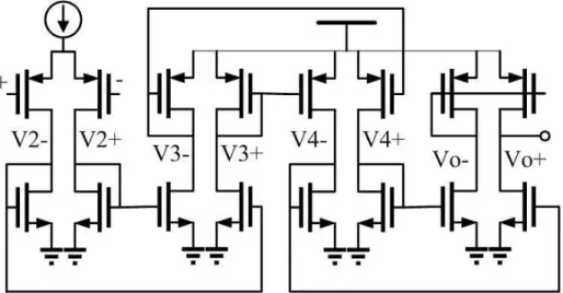
4.2.1 Frequency MultiplierThe frequency multiplier in the last section suffers from large parasitic capacitance on the internal node X and Y with the increasing of multiplication factor. Another frequency multiplier architecture is illustrated in Fig.4.2.1. The drawback of large internal parasitic capacitance is overcome. The blocks of the frequency multiplier are described as follows.
Fig.4.2.1 A Programmable Frequency Multiplier ◆
◆ ◆
◆ Transition detector
A single transition detector cell consists of a 3-input NAND and an inverter. Eight cells are chosen for programmable frequency multiplication that is controlled by the select signal Si.
◆ ◆ ◆
◆ AND logic
against the pull-up path (i.e. PMOS in parallel) is not a wise choice. Besides, the improper arrangement of the signal affect the “AND” results (see Fig.4.2.2). The 2-input symmetric NAND in accompany with the arrangement of the signals ensure the correct function.
A
k1
k2
k3
k4
k5
k6
k7
k8
(a)
a1
a2
y
x
y
i
j
Fig.4.2.2 (a) AND logic with straight forward signal arrangement. (b) AND logic with alternative signal arrangement. (c) The schematic of signal propagation failure [14]. ◆
◆ ◆
◆ Toggle-pulsed latch (TPL)
The operation of TPL (see Fig.4.2.3) is as follows. The short pulse signal A is fed to TPL and Ab is the inverted signal of A. M1 is used to prevent the node X from voltage drop of Vth and enhances the setup time when the node X changes from “low” to “high”. The maximum speed of TPL is limited by the total delay of three inverters (Inv1-Inv3). The delay of the signal path can be characterized by a logic effort equation (eq. (4.1)). For simplicity, the maximum operation frequency can be roughly estimated by eq. (4.2) while neglecting the delay of M2 and Inv1~Inv3 can be treated as a ring oscillator suppose M2 always turned on.
p gb
td N d fQ ‧ ‧2 1 = (4.2)
where d is total delay, g is logic effort, b is the number of branch, p is the parasitic delay, N is the number of stage, and td is the delay time of an inverter.
2 1 1 1 + = =‧ d , GHz ps fQ 2.1 40 3 4 1 ≅ = ‧ ‧ . Fig.4.2.3 TPL 4.2.2 Encoder
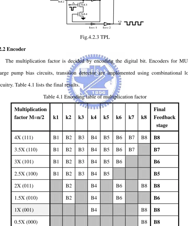
The multiplication factor is decided by encoding the digital bit. Encoders for MUXs, charge pump bias circuits, transition detector are implemented using combinational logic circuitry. Table 4.1 lists the final results.
Table 4.1 Encoding table of multiplication factor
Multiplication factor M=n/2 k1 k2 k3 k4 k5 k6 k7 k8 Final Feedback stage 4X (111) B1 B2 B3 B4 B5 B6 B7 B8 B8 3.5X (110) B1 B2 B3 B4 B5 B6 B7 B7 3X (101) B1 B2 B3 B4 B5 B6 B6 2.5X (100) B1 B2 B3 B4 B5 B5 2X (011) B2 B4 B6 B8 B8 1.5X (010) B2 B4 B6 B6 1X (001) B4 B8 B8
4.2.3 Timing match
The ideal multi-phase distribution is illustrated in Fig.4.2.4(a). Total delay of the delay path is given by eq. (4.3).
CLK VCDL
tot N t t
t = ‧ = (4.3)
The final feedback stage of VCDL is changed for different frequency multiplications. Therefore, a MUX is added in the delay path, and the total delay is given by eq. (4.4) resulting in the timing offset every N cycles (see Fig.4.2.4(b)).
CLK MUX VCDL
tot N t t t
t = ‧ + = (4.4)
The extra delay cell and MUX are added to cancel the timing offset problem (see Fig.4.2.4(c)).
4.3 Simulation results
◆ Fig.4.3.1 PFD operation when the reference signal and feedback signal are in phase
◆ Fig.4.3.3 PFD operation when the reference signal lags feedback signal @ 300MHz
◆ Fig.4.3.4 Behavior of charge pump
◆ Fig.4.3.6 VCDL delay time versus control voltage sweep
◆ Fig.4.3.7 Corner simulations of the VCDL B8 delay time versus control voltage sweep
- Fig.4.3.8(b) Locking process overview
- Fig.4.3.9 Initial state
◆ Fig.4.3.11 Transition detector and AND logic operates at 300MHz
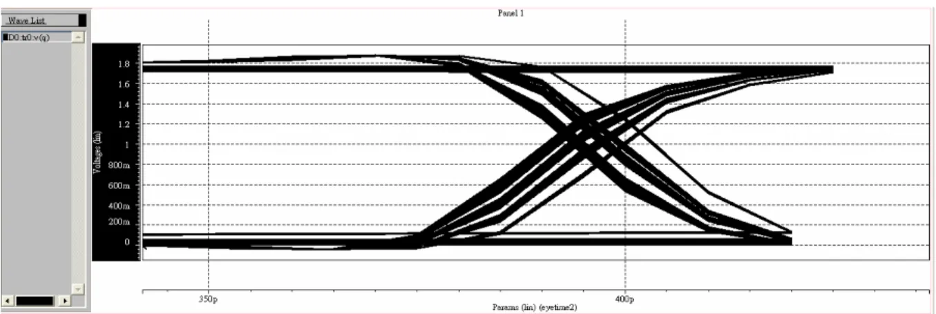
◆ Jitter simulation measurement by eye diagram
The jitter of multiplied output can be observed by truncating the signal every N clock cycle. The method is shown in Fig.4.3.12 to clearly observe the timing width of the clock jitter.
◆ Fig.4.3.13 Eye diagram of the output clock operates at 1200MHz (4X)
◆ Fig.4.3.14 Dynamic frequency scaling of 0.5X, 1X, 2X, 4X
Fig.4.3.16 Output clock jitter due to DLL phase offset of Fig.4.3.15 @ 1200MHz (4X)
Table 4.2 Performance Summary Performance Table
Process TSMC 0.18µm CMOS Mixed 1P6M 1.8&3.3V
Power supply 1.8v & 3.3v(for CP, PD, and Voltage buffer)
Operating frequency Min- 150MHz (fref=300MHz, multiplication factor=0.5X)
Max- 1.2GHz (fref=300MHz, multiplication factor=4X)
Peak to peak jitter (Simulation result)
< 3ps @ 1.2GHz (TT) < 20ps @ 1.2GHz (FF)
< 20ps @ 1.2GHz (SS)
Duty cycle ratio ~ 50 ± 1.1% (TT)
~ 50 ± 6% (FF) ~ 50 ± 7.5% (SS)
Die area 0.85 x 0.61mm2
Chapter 5
Experimental Results
5.1 Input Clock Consideration
Because DLL has no immunity against the input clock jitter, two strategies of low jitter clock generation are developed to offer a clean input clock (see Fig.5.1.1-2). Strategy I, instead of using square wave, employs the differential sinusoidal wave from the signal generator and a regulated input buffer to achieve high supply noise immunity. The cross-coupled topology in accompany with the few inverter chain buffer stages convert the sinusoidal wave to square wave fed to DLL. Strategy II employs a crystal oscillator and a PLL to generate the input signal. The crystal oscillator has very high quality so as to generate a clean clock signal with the fixed resonance frequency around hundreds of kHz up to several decade of MHz, then followed by a PLL to generate hundreds of MHz clock for DLL usage.
Fig.5.1.1 Low jitter clock generation - Strategy I.
5.2 Output Buffer Design
Taper buffer (see Fig.5.2.1) is chosen as the output buffer for the output clock. The physical size between the successive taper buffer stages are gradually enlarged by the calculation of logic effort to obtain the optimal driving ability.
Fig.5.2.1 Taper buffer
5.3 Layout Consideration
The variance of the performance of the DLL-based clock generator is extremely affected by layout. To minimize the phase offset due to layout, the following part should notice: Dummy cell insertion to ensure the same loading between different clock stages in VCDL, isolation buffers, transition detector, and AND logic. For higher current mirror precision, long channel devices are chosen and common-centroid layout is employed. Separation of the analog and digital supply voltages can reduce the noise of sensitive circuits. Double guard ring should be inserted surrounding and between the special devices such as charge pump, power regulator, high noise or high power circuitry [15]. Capacitor matching is violated by overetching (see Fig.5.3.1) when the capacitors are not unit-sized. Skills against process variation are employed [16] by realizing a nonunit-sized capacitor with a specific perimeter-to-area ratio. The ideal and the true capacitor sizes are given by eq. (5.1) and eq. (5.2) separately. The error in the true capacitance is approximated by eq. (5.3) assuming the error is small. 1 1 1 C x y A t C OX OX OX I = = ε (5.1) ) 2 )( 2 ( 1 1 1 1 y C x e y e x C CT = OX T T = OX − ∆ − ∆ (5.2) 2 ≅− ∆ + ∆ + + ∆ − = − = ∆
The relative error εr in the capacitor is given by eq. (5.4). The ratio of two capacitors is
determined by eq. (5.5). The result shows that the ratio K is constant when their perimeter-to-area ratios are kept the same (i.e., εr1=εr2).
1 1 1 1 ) ( 2 y x y x e C C I T r + ∆ − ≅ ∆ = ε (5.4) ) 1 ( ) 1 ( 2 2 1 1 2 1 r r T T C C C C K ε ε + + = = (5.5)
Fig.5.3.1 Capacitor errors due to overetching.
5.4 Experimental Results
The proposed DLL-based clock generator for dynamic frequency scaling has been integrated in a 0.18µm 1P6M CMOS process. The die microphotograph is shown in Fig.5.4.1. The total die area of the chip is 0.85 x 0.61 mm2.
Fig.5.4.1 Die microphotograph
5.5 Test Setup
◆ ◆ ◆ ◆ PCB DesignThe maximum frequency of a FR4 double-side printed board can up to 3GHz is chosen. To reduce the power supply noise, LM317 is used and the SMD capacitors are placed as closed as possible. The regulated supply voltage is given by eq. (5.4).
) 1 ( 25 . 1 1 2 R R Vreg = + (5.4)
In advance, by adding the bypass filter network to the regulator output can attenuate both low-frequency noise with large amplitudes and high-frequency noise with small amplitudes [17]. The analog and digital grounds are in split copper planes and joined with a short segment of trace to give a common reference potential.
Fig.5.5.2 PCB photo ◆ Measurement Equipment
The measurement setup of the die under test (D.U.T) is shown in Fig.5.5.2. Agilent E3610A power supply
Agilent E8257D 250kHz to 40GHz PSA analog signal generator Agilent 54832D Mixed-signal Oscilloscope
5.6 Error-shooting
The improper layout of the taper buffer leads to the degradation of the driving capability due to too large parasitic resistance in the output. By the way, the post-simulation of the clock generator should contain the parasitic resistance extraction from the taper buffer and the PAD. We should note that the simulation result becomes suspected once exceeding the effective operating range of the model that is offered from the foundry. Especially in the dual supply design, the interface of 3.3V and 1.8V devices may exceed the operating range and is suggested to configure as shown in Fig.5.6.1.
Fig.5.6.1 Interface of VCDL and isolation buffer.
To eliminate the body effect, the bulk of the delay cell is tied to the source. However, large current consumption of the chip is suspected to latch-up problem. Unfortunately, the latch-up phenomenon cannot be detected in the simulation.
We can prevent latch-up by layout according to the technology documents:
- Any NW without direct connection to VDD and with hot OD inside it should be surrounded by double guard ring.
Table 5.1 Performance Comparison (continued) JSSC, 2000, Paul .R Gray[2] ISCAS, 2001[19] JSSC, 2001 Michael P. Flynn[20] ISSCC, 2002 Ramin Farjad-rad [6] JSSC,2002 Chulwoo Kim, Sung-Mo (Steve) Kang[13]
Technology 0.35um 0.8um 0.5um 0.18um 0.35um
Input clock Frequeny
range
100MHz 100MHz N/A N/A N/A
Operating frequency range 900MHz 200MHz~ 800MHz (Max:1GHz) 2V:600MHz~ 1GHz 3.3V:900MHz~ 1.6GHz 200MHz~ 2GHz 120MHz~ 1.1GHz Multiplication factor 9X 2X~8X N/A 4X,5X, 8X,10X 0.5X~4X Peak to peak jitter N/A N/A <20ps 15.6ps ±7.28ps Die area mm2 1.2x1 N/A 0.6 0.05 0.07 Power consumption 130mW N/A 138mW 12mW 42.9mW
(Continued) JSSC, 2004 R. Farjad-rad [21] VLSI Systems ,2004[22] JSSC, 2006 Chulwoo Kim[14] Master Thesis, 2005 [23] This work
Technology 0.13um 0.25um 0.35um 0.18um 0.18um
Input clock Frequeny range N/A 120MHz (100MHz~ 150MHz) 240MHz~ 450MHz 220MHz ~320MHz 200MHz ~330MHz (300MHz) Operating frequency range N/A (2GHz) 1.2GHz 120MHz~ 1.8GHz 1.16GHz 220~320MHz 440~660MHz 880~1.28MHz 150MHz~ 1.2GHz Multiplication factor 1X~10X 7X~10X 0.5X~4X 1X,2X,4X 0.5X~4X Peak to peak jitter 15ps N/A ±6.6ps <58.4ps N/A Die area mm2 N/A 1.06x1 0.07 0.86x0.79 0.85x0.61 Power consumption N/A 52.2mW 86.6mW 50.4mW 28.3mW
Chapter 6
Conclusions
6.1 Final Discussion
In this section, we discuss the internal co-relation as a whole for the final look of this work.
The programmable multiplication factor using previous frequency multiplication method gains 0.5X-based resolution of frequency multiplication factor and the frequency multiplication factor up to 4X in this work. Someone may try to promote the operation frequency of output clock by increasing the total number of delay stages and it seems work in this mechanism. However, the maximum operation frequency is also limited by the frequency multiplier itself whatever we increase the multiplication factor as analyzed before. Also, in increasing of delay stages degrades the jitter performance of DLL and the jitter must be estimated and controlled under an acceptable range according to their applications. The input clock range is limited by the building blocks in DLL, such as the linear range of PD, and the delay range of VCDL. The former is mainly decided by the circuit architecture, and the latter is the trade-off between delay range and noise accumulation. The settling behavior is decided by the loop bandwidth of DLL and the choice of the loop bandwidth also affects the phase noise performance, area, and power dissipation.
6.2 Epilogue and Future Work
A wide frequency operating range clock generator for dynamic frequency scaling is presented and achieves 0.5X-based frequency multiplication factors. This work is devoted to reach the compromise between the trade-off of multi-dimensional parameters, such as bandwidth, operating range, stability, noise, speed, supply voltage, etc. The dominant problem of each building block is taken into consideration and has tackled by the system analysis, circuit design techniques, and layout skills.
For low supply voltage operation in deep submicron process, the low jitter clock generator with wide frequency operating range will be more challenged. There are some suggestions for the future development. Since robustness is the best advantage of the digital circuit, all digital DLL-based clock generator with highly noise immunity and area-efficient will be the next star as long as the timing resolution can be promoted. Recently, a programmable duty cycle correction loop is a popular research topic. To combine clock generation with duty cycle adjustment can be another direction. Finally, also the most difficult issue is to generate much higher fractional-N resolution of frequency multiplication factor.
[1] B.Kim,T.C.Weigandt,andP.R.Gray, “PLL/DLL system noise analysis for low-jitter clock synthesizer design,” in Proc. Int. Symp. Circuits and Systems, London, U.K., June 1994. [2] G. Chien and P. R. Gray, “A 900 MHz local oscillator using a DLL-based frequency multiplier technique for PCS applications,” in IEEE Int. Solid-State Circuits Conf. Dig. Tech. Papers, Feb. 2000, pp. 202-203.
[3] Rusu, S.; Tam, S , et al “A 65-nm Dual-Core Multithreaded Xeon® Processor With 16-MB L3 Cache” IEEE J. Solid-State Circuits, vol. 42 no. 1, pp. 17-25, Jan. 2007.
[4] Yuan Chen; Yu-Wei Lin; Yu-Chi Tsao; Chen-Yi Lee, “A 2.4-Gsample/s DVFS FFT Processor for MIMO OFDM Communication Systems” IEEE J. Solid-State Circuits, vol. 43 no. 5, pp. 1260-1273, May. 2008.
[5] Lee, M.-J.E., Dally, W.J., et al “Jitter transfer characteristics of delay-locked loops - theories and design techniques” IEEE J. Solid-State Circuits, vol. 38 no. 4, pp. 614-621, April. 2003.
[6] Farjad-Rad, R, et al “A 0.2-2 GHz 12 mW multiplying DLL for low-jitter clock synthesis in highly-integrated data communication chips” in IEEE Int. Solid-State Circuits Conf. Dig. Tech. Papers, Feb. 2002, pp. 76-77.
[7] Maneatis, J.G “Low-jitter process-independent DLL and PLL based on self-biased techniques” IEEE J. Solid-State Circuits, vol. 31 no. 11, pp. 1723-1732, Nov. 1996.
[8] Van de Beek, et al “Low-jitter clock multiplication: a comparison between PLLs and DLLs.” Circuits and Systems II: Analog and Digital Signal Processing, IEEE Transactions on vol. 49, no. 8, pp. 555 – 566, Aug. 2002.
[9] Beomsup Kim, Weigandt, T.C., Gray, P.R., “PLL/DLL system noise analysis for low jitter clock synthesizer design.” Circuits and Systems, 1994. ISCAS '94., 1994 IEEE International Symposium on vol.4, pp. 31-34 , 30 May-2 June 199
[10] Maneatis, J.G “Low-jitter process-independent DLL and PLL based on self-biased techniques” in IEEE Int. Solid-State Circuits Conf. Dig. Tech. Papers, Feb. 1996, pp. 130-131.
[11] M. Lee, W. Dally, and P. Chiang. “Low-power area-efficient high-speed I/O
circuit techniques.” IEEE J. Solid-State Circuits, vol.35, no. 11, pp. 1591 -1599, Nov. 2000. [12] A 2.5 Gbps CMOS data serializer
[13] Chulwoo Kim; In-Chul Hwang; Sung-Mo Kang; “A low-power small-area ±
7.28-ps-jitter 1-GHz DLL-based clock generator” in IEEE Int. Solid-State Circuits Conf. Dig. Tech. Papers, Feb. 2002, pp. 142-143.
[14] Jin-Han Kim, Young-Ho Kwak, Seok-Ryung Yoon, Moo-Young Kim, Soo-Won Kim, Chulwoo Kim, “A 120-MHz–1.8-GHz CMOS DLL-Based Clock Generator for Dynamic Frequency Scaling” in IEEE Int. Solid-State Circuits Conf. Dig. Tech. Papers, Feb. 2006, pp. 516-517.
[15] TSMC 0.18um technology document.
[16] Johns-Martin, Design of Analog Integrated Circuits and Systems, 1997
[17] De-Wen Liao, Low-Noise Delta-Sigma Frequency Synthesizers for DTV and WIMAX Applications, Department of Communication Engineering National Chiao Tung University, Dec. 2007.
[18] Guyeon Wei, Mark Horowitz, et al “Adaptive bandwidth DLLs and PLLs using regulated supply CMOS buffers,” in Symp. VLSI Circuits Dig. Tech. Papers, Jun. 2000, pp. 124–127. [19] Aguiar, R.L.; Santos, D.M.,“Oscillatorless clock multiplication”, IEEE International Symposium on Circuits and Systems (ISCAS), vol. 4, pp.630-633, May 2001.
[20] D. J. Foley and M. P. Flynn,“CMOS DLL-based 2-V 3.2-ps jitter 1-GHz clock synthesizer clock synthesizer and temperature-compensated tunable oscillator,”IEEE J. Solid-State Circuits, vol. 36, pp. 417-423, Mar. 2001.
[21] R. Farjad-Rad, A. Nguyen, et al“A 33-mW 8-Gb/s CMOS clock multiplier and CDR for highly integrated I/Os,” IEEE J. Solid-State Circuits, vol. 39, no. 9, pp. 1553–1561, Sep. 2004.
DLL-based frequency multiplier for wireless applications”, IEEE Transactions on Very Large Scale Integration (VLSI) Systems, vol.12, pp.1377-1381, Dec. 2004.
[23] Shu-Ming Chang
![Table 5.1 Performance Comparison (continued) JSSC, 2000, Paul .R Gray[2] ISCAS, 2001[19] JSSC, 2001 Michael P](https://thumb-ap.123doks.com/thumbv2/9libinfo/8465543.183336/56.892.117.810.124.1009/table-performance-comparison-continued-jssc-paul-iscas-michael.webp)
