國
立
交
通
大
學
電機學院 電子與光電學程
碩
士
論
文
具有交錯型遲滯延遲元件的低功耗數位控制振盪器
A low power digitally controlled oscillator based on
interlaced hysteresis delay cells
研 究 生:游佳融
指導教授:李鎮宜 教授
具有交錯型遲滯延遲元件的低功耗數位控制振盪器
A low power digitally controlled oscillator based on
interlaced hysteresis delay cells
研 究 生:游佳融
Student:Chia-Jung Yu
指導教授:李鎮宜 教授
Advisor:Prof. Chen-Yi Lee
國 立 交 通 大 學
電機學院 電子與光電學程
碩 士 論 文
A Thesis
Submitted to College of Electrical and Computer Engineering National Chiao Tung University
in partial Fulfillment of the Requirements for the Degree of
Master of Science in
Electronics and Electro-Optical Engineering September 2011
Hsinchu, Taiwan, Republic of China
I
具有交錯型遲滯元件的低功耗數位控制振盪器
研究生: 游佳融 指導教授: 李鎮宜 國立交通大學 電機學院 電子與光電學程 碩士班摘要
隨著晶片製程技術的進步,可攜式產品變得越來越熱門。在可攜式產品應用中 功耗就變成很重要的問題。全數位鎖相迴路在通訊系統中應用很廣。在全數位鎖相 迴路電路裡,數位控制振盪器是一個關鍵性的元件。數位控制振盪器的操作頻率和 靈敏度可以影響整個全數位鎖相迴路的性能,不只如此,功耗的比例是全數位鎖相 迴路 50%以上。設計一個低功耗的全數位鎖相迴路,降低數位控制振盪器的功耗是 一個非常有效率的方法。 本論文將會提出一個具有低功耗的新型延遲元件。這個交錯型遲滯延遲元件可 以節省電源,達到低功耗,小面積和高效能。數位控制振盪器架構採用串聯和改良 型二權重式架構,但是這個架構會延生出一些問題,例如最快頻率限制和突波 (glitch)問題。這些問題在本論文中會被一一解決。我們使用標準元件庫來設計整 個晶片,並利用合成軟體及自動佈局工具實現電路,最後以 90 奈米 1P9M 標準 CMOS 製程來完成晶片。 本論文提出的交錯型遲滯延遲元件和標準元件(AND gate)相比 可節省 87%的功耗,本論文提出的數位振盪器為 480MHz,功率消耗為 128uW。II
A low power digitally controlled oscillator based
on interlaced hysteresis delay cells
Student: Chia-Jung Yu Advisors: Dr. Chen-Yi Lee Degree Program of Electrical and Computer Engineering
National Chiao Tung University
ABSTRACT
As technology advances, portable devices become more and more popular. In portable devices, the power consumption becomes an important design issue. An all digital phase lock loop (ADPLL) has been widely used in frequency synthesizer and communication systems. Digitally controlled oscillator (DCO) is the key component of performance and power of ADPLLs. The operated range and delay resolution of the DCO dominate jitter and output range of an ADPLL. A DCO occupies over 50% power consumption of an ADPLL. Power reduction on a DCO can effectively cut down the overall ADPLL power.
This work proposes a novel delay cell in low power applications. The interlaced
hysteresis delay cell has low power consumption, small area and high quality. The DCO
structure uses the modified binary-weighted delay stage and cascade-stage structure.
However, the disadvantages of the structure are the serious glitches and the limited fastest
frequency. The proposed solution uses a synchronization cell to avoid glitches. Moreover,
the proposed DCO also increases the fastest frequency. This chip is implemented with
standard cell library by synthesis and auto place-and-route tools. The low power DCO is
fabricated in 90nm 1P9M standard CMOS process. The proposed IHDC reduces over 87%
power consumption on the standard DCO which is based on AND gates. The power
III
誌 謝
在這一段研究的過程中,我首先要感謝我的指導老師李鎮宜教授。老師在研究 上給我很多的建議和方向並且總是鼓勵我,讓我用樂觀積極的態度面對我的研究。 另外,要感謝我的口試委員:黃威教授、莊景德教授和鍾菁哲教授,在百忙當中來 參加我的口試。再來要謝謝指導我的學長余建螢,在我研究遇到瓶頸時給我一些良 好的建議並教我用不同的角度觀察問題,在他身上我不僅學習到新知,更看到追求 知識的真善美。另外也要感謝實驗室的學長及同學:燦文學長、書餘學長、偉豪學 長、秉原和子均。你們給我的建議跟關懷我都深深銘記在心。最後感謝學弟妹姿儀, 佩妤和恕平的幫忙,讓我能夠順利的完成口試。 在 Si2 Lab 裡, 每個人都非常友善,讓我重拾久違的校園生活。在此感謝給過 我建議的人更謝謝給我鼓勵的人,有了你們的幫忙,我才能順利完成碩士論文。最 後謝謝我的父母,給了我最大的支持跟信任,心中感念無以回報。IV
CONTENTS
1 Introduction ... 1
1.1 Motivation ... 1
1.2 Thesis organization ... 3
2 Interlaced hysteresis delay cell ... 4
2.1 Analysis of different delay cells ... 4
2.2 Concept of the IHDC ... 6
2.3 Stack enhanced IHDC ... 8
2.4 Characteristic of the IHDC ... 11
2.4.1 Background ... 11
2.4.2 IHDC characteristics – the propagation time ... 13
2.4.3 IHDC characteristics – power consumption ... 14
2.4.4 Summary ... 14
3 Digitally controlled oscillator... 17
3.1 Basic concepts of DCOs ... 17
3.2 Different approaches for DCOs ... 17
3.2.1 Linear architecture ... 18
3.2.2 Matrix tri-state architecture ... 19
3.2.3 Cascade stage architecture ... 19
3.2.4 Binary-weighted architecture ... 20
3.2.5 Proposed architecture ... 22
V
3.4 Structure of proposed DCO ... 28
3.5 Simulation results and layout ... 30
4 Chip Implementation ... 38
4.1 Architecture of the ADPLL ... 38
4.1.1 Phase / Frequency Detector ... 39
4.1.2 Control unit ... 40
4.2 Summary ... 40
5 Conclusion ... 42
5.1 Conclusion ... 42
VI
LIST of FIGURES
Figure 1 hysteresis delay cell of (a) Dokic architecture (b) Sarawi architecture ... 4
Figure 2 interlaced hysteresis delay cell ... 6
Figure 3 bypass circuit block diagram ... 7
Figure 4 bypass schematic (a) type 1 (b) type 2 ... 8
Figure 5 enhanced IHDC (a) level 3 (b) level 3 with numeral connection (c) level 4 (d) level 5 ... 10
Figure 6 level 3 IHDC includes the bypass circuit ... 11
Figure 7 IHDC switching model (a) circuit (b) RC switch model equivalent of the fall time (c) RC switch model equivalent of the rise time ... 13
Figure 8 different delay cells of (a) Inverter (b) AND gate (c) Dokic type HDC (d) Sarawi type HDC (e) IHDC - level 2 ... 16
Figure 9 a typical ring-oscillator ... 18
Figure 10 a linear architecture ... 18
Figure 12 an improved DCO architecture ... 19
Figure 13 a binary-weighted DCO architecture ... 20
Figure 14 system block diagram of (a) the linear and (b) the binary-weighted ... 21
Figure 15 block diagram of (a) the modified binary-weighted delay stage (b) the cascade-stage structure ... 23
Figure 16 glitch waveform ... 24
Figure 17 the traditional solution for glitches ... 24
Figure 18 from short delay path to long delay path: (a) circuits (b) waveform (c) analysis for changing codeword ... 25
Figure 19 from long delay path to short delay path: (a) circuits (b) waveform (c) analysis for changing codeword ... 26
VII
Figure 20 a three bits binary-weighted DCO (a) circuits (b) equivalent circuits (c) waveform
... 27
Figure 21 proposed solution for glitches (a) circuits (b) waveform ... 27
Figure 22 proposed DCO architecture with the cascade stage ... 28
Figure 23 loading capacitance and resistance (a) the equivalent circuit (b) the proposed delay cell in 1st fine tuning stage ... 30
Figure 24 loading capacitance and resistance (a) the equivalent circuit (b) the proposed delay cell in 2nd fine tuning stage ... 30
Figure 25 proposed DCO block with the cascade stage ... 31
Figure 26 simulation of the DCO period versus the second fine code ... 32
Figure 27 simulation of the DCO period versus the first fine code ... 33
Figure 28 simulation of the DCO period versus the second coarse code in PVT variations .... 34
Figure 29 simulation of the DCO period versus the first coarse code in PVT variations ... 35
Figure 30 simulation of the DCO period of coarse code and fine code in PVT variations ... 36
Figure 31 layout of the proposed DCO ... 36
Figure 32 block diagram of the proposed ADPLL ... 38
Figure 33 modified 3-state PFD architecture ... 39
Figure 34 simulation result of the PFD circuit ... 39
Figure 35 layout of the proposed ADPLL ... 41
VIII
LIST of TABLES
Table 1 comparison with the different type of delay cells ... 16
Table 2 comparison table between the linear and binary-weighted architecture ... 21
Table 3 step and range of each tuning stage ... 31
Table 4 simulation result of the second fine tuning stage in the proposed DCO ... 31
Table 5 simulation result of the first fine tuning stage in the proposed DCO ... 33
Table 6 simulation result of the second coarse tuning stage in the proposed DCO ... 34
Table 7 simulation result of the first coarse tuning stage in the proposed DCO ... 35
Table 8 comparison with existing DCOs ... 37
1
1
Introduction
1.1 Motivation
As technology advances, the demands of portable and multi-function devices increase like mobile phones. The portable devices need a small area. The system-on-a-chip (SoC) is widely used in a small area design. The power consumption in portable devices becomes important in a SoC design, as power dissipation relates directly to battery life. Phase-locked loops (PLLs) have been widely used in frequency synthesizers, communication systems and microprocessors.
A traditional PLL which consists of analog components is difficult to be integrated in noisy digital environments and not easily portable to different process technologies. A voltage-controlled oscillator (VCO) is a basic component in an analog PLL. The oscillation frequency of the VCO is controlled by the voltage. As the supply voltage decreases, VCO gain and an operating frequency range need to be traded off [12] [19]. Furthermore, a charge-pump circuit has a serious leakage current problem in more advanced process [20]. As a result, it needs more efforts to design analog PLLs in SoC with low supply power and advanced process. A digital design does not utilize any passive components. It can be easily integrated into digital and low-supply voltage system. The digital way is reusable as an intellectual property (IP). It can reduce design time and design complexity by using verilog (or VHDL) hard-ware-description language. The circuit layout is generated by using an auto placement and routing (APR) tools. It reduces time-to-market for a new design. The cell-based all-digital approach benefits easy portability for different process, high integration in SoC design, good immunity against switching noise and low leakage current in low voltage supply. In addition, the digital design is easily reconfigurable. For these reasons, an all-digital phase-locked loop (ADPLL) is very attractive to designers in a portable device. The ADPLL is becoming
2
increasingly popular. It overcomes the analog limitations and enhances the traditional PLL functionality.
The digitally controlled oscillator (DCO) is a kernel component in the ADPLL module. The performance and power consumption of the DCO dominate the overall ADPLL. The operation range and delay resolution of a DCO are related to the jitter performance and output range of the ADPLL. Over 50% power consumption in an ADPLL comes from a DCO [11]. Power reduction on a DCO can effectively cut down the overall ADPLL power.
The most power consumption of an ADPLL comes from the DCO. In order to reduce power consumption, this work addresses (i) a set of hysteresis delay cells (HDCs) with novel structures(ii) a binary-weighted (BW) delay stage architecture which largely reduces the DCO area with the proposed HDC set, (iii) a cascade-stage structure with coarse and fine tuning stage can provide high resolution, wide range and small number of delay cells. The proposed DCO can achieve linearity and low power. The proposed HDC interlaces the delay path with shared current. The proposed delay cell with shared current has a longer delay time. It replaces several standard delay cells to reduce power consumption and circuit complexity. In the cascade-stage DCO, the coarse tuning stage has a larger propagation time of a delay cell. It can use less delay cells to cover the range of operation frequency. The fine tuning stage uses a smaller propagation time of a delay cell to provide the resolution of the DCO. A cascade-stage DCO provides high resolution, wide range and small number of delay cells at the same time. The binary-weighted DCO can largely reduce the number of cells. However, the glitch is serious in a binary-weighted delay stage. The synchronization cells are proposed to avoid glitches. The proposed DCO overcomes the challenge in the power reduction and make the proposed DCO a preferred choice in power-thirsty or battery-operated systems.
3
1.2 Thesis organization
The organization of this thesis is as follows: In Chapter 1, we describe the motivation. Chapter 2 introduces different delay cells and the proposed interlaced hysteresis delay cell. In Chapter 3, general structures of DCOs are discussed, and the proposed binary-weighted cascade stage structure is presented. The binary-weighted stage DCO may generate glitches due to the path selection architecture. We discuss the detailed timing of glitches and propose a solution. The simulation result of the proposed DCO is presented. Chapter 4 applies the proposed low power DCO in an application example of a 480MHz ADPLL. Finally, the conclusions are given in Chapter 5.
4
2
Interlaced hysteresis delay cell
2.1 Analysis of different delay cells
The ring oscillator is composed of serial delay cells. The output period is consisted of each propagation time of the inverter. A variable number of delay cells implement a variable propagation time. The basic delay cell is an inverter (INV) and an AND gate in the standard library. Those digital cells can be easily used and quickly re-designed to different process technologies. The following composition discusses some other different delay cells.
Schmitt trigger is a waveform shaping circuit exploiting two threshold voltages. A Schmitt trigger circuit operates on the different threshold values when an input signal level increases and decreases. The circuit has hysteresis characteristics in changes of the output signal level with respect to changes in the input signal level. This dual threshold action creates an extra delay. This phenomenon is called hysteresis. The hysteresis delay cell is designed based on a Schmitt-trigger circuit. There are two common HDCs
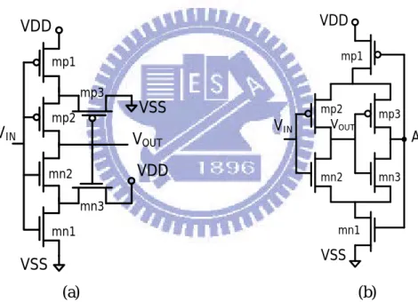
Figure 1 hysteresis delay cell of (a) Dokic architecture (b) Sarawi architecture
(a) (b) VIN VOUT VSS VDD VSS VDD mp1 mp2 mp3 mn1 mn2 mn3 VIN VOUT VDD VSS A mn1 mp1 mn2 mp2 mp3 mn3
5
including Dokic and Sarawi architecture as shown in Figure 1(a) [15] and (b) [16], respectively.
A Schmitt cell of Dokic architecture [15] is shown in Figure 1(a). When the initial input voltage is equal to VDD, mp1 and mp2 are in cut off region; mn1 and mn2 are turned on. The output signal is equal to ground, leading to mn3 in cut off region and mp3 in saturation region. When the input signal decreases to the low threshold level, the transistors mp1, mp2 and mp3 are turned on. Then, a charging path changes the output signal from ground to VDD. Oppositely, the input signal increases to the high threshold level. The transistors mn1, mn2 and mn3 turn on. The discharging path changes the output signal from VDD to ground. The Schmitt cell of Dokic type has a short current path when transistors switch. That increases power consumption.
Figure 1(b) illustrates the Schmitt cell of Sarawi architecture [16] which is designed by inverter chain internally cascaded with a footer transistor and a header transistor. This cell uses a feedback circuit to cause larger delay time and smaller normalized power consumption. When the initial input signal is equal to VDD, the transistors mn1, mn2 and mp3 are turned on. The transistors mp1, mp2 and mn3 are then turned off. When the input signal decreases to the low threshold level, the transistor mp2 is turned on and the transistor mn2 is turned off. The transistor mp3 is turned off and the transistor mn3 is turned on. The point A is a weak logic zero. As the input voltage rises, the output signal switches from the high level to the low level. The point A changes from a weak logic zero to a weak logic one. This cell of Sarawi architecture avoids short current path, leading in lowering power consumption. However, the point A is the week logic one or zero, leading to have larger PVT variations. The PVT variations cause an unstable propagation time and output frequency. The output range must cover the PVT variations. The larger PVT variations need a larger output range to cover it. The larger PVT variations increase the number of delay cells in the same output frequency.
6
Therefore, the larger PVT variations cause the larger power consumption.
2.2 Concept of the IHDC
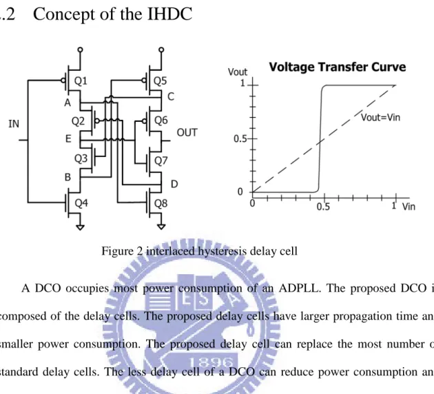
A DCO occupies most power consumption of an ADPLL. The proposed DCO is composed of the delay cells. The proposed delay cells have larger propagation time and smaller power consumption. The proposed delay cell can replace the most number of standard delay cells. The less delay cell of a DCO can reduce power consumption and area. The hysteresis delay cell of Sarawi architecture has the larger PVT variations due to a weak point. Every connected point of IHDC can achieve a strong VDD or a strong GND. As a result, the PVT variations of the proposed IHDC are smaller as an inverter of a standard cell.
The proposed interlaced hysteresis delay cell (IHDC) is shown in Figure 2. The IHDC uses diagonal lines to connect two cascode cells. Two cascaded transistor chains with shared power current. Moreover, the delay paths are extended to share the same power current. The IHDC not only uses the shared power supply to extend the propagation time, but also avoids short-circuit current. When the input signal switches, both nMOS and pMOS networks momentarily turn on at the same time. The short-circuit current occurs when input signal switches. If nMOS and pMOS do not switch at the
7
same time, the short-circuit current will not happen.
The IHDC is comprised of the pMOS (Q1, Q2, Q5 and Q6) and the nMOS (Q3, Q4, Q7 and Q8). The cascode inverters supply a shared source. Figure 2 shows the DC characteristics of the IHDC with the voltage transfer characteristic (VTC). This is obtained by varying the input voltage Vin in the range from 0V to VDD and finding the output voltage Vout. As a low potential level applies to the input, the pMOS (Q1) is turned on and nMOS (Q4) is turned off. The pMOS (Q1) will begin to charge until the source of Q1 reaches high potential, which forces the nMOS (Q8) to be turned on.
The pMOS (Q2) is sequentially turned on by the fall of the gate potential. The output is charged by the series-connected nMOS (Q7) to decrease the potential of this output. As a high potential level supplies to the input, the pMOS (Q1) is turned off and the nMOS (Q4) is turned on. The nMOS (Q4) will begin to discharge until the drain of Q4 reaches the low potential, which forces the pMOS (Q5) to be turned on. The nMOS (Q3) is sequentially turned on by the rise of the gate potential. The output is charged by the series-connected pMOS (Q6) to increase the potential of this output. From the interlaced path and the shared power source, the IHDC cell is able to increase the propagation time and reduce the consumption power.
Figure 3 bypass circuit block diagram
IN OUT Q1 Q2 Q3 Q4 Q5 Q6 Q7 Q8 A B C D
8
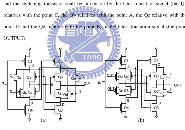
The bypass circuit (BC) is a charge redistribution circuit, as shown in Figure 3. The bypass circuit is able to enhance large propagation time, jitter performance and low power consumption. The four points (point A, B, C, D) shall store the impermanent charge when the input is in transition. The impermanent charge causes a weak logic at point A, B, C, D and reduces the jitter performance of the IHDC. The bypass circuit can eliminate the impermanent charge. The bypass circuit uses the relative point to control the switch timing. There are many type of the bypass circuit, as shown in Figure 6. The switching transistor is controlled by backward signal. When the input signal is from the low potential to the high potential, the point A, B, C, D strong the impermanent charge and the switching transistor shall be turned on by the later transition signal (the Qa relatives with the point C, the Qb relatives with the point A, the Qc relative with the point D and the Qd relative with the point B) or the latest transition signal (the point OUTPUT).
2.3 Stack enhanced IHDC
The concept of the enhanced IHDC creates a delay cell which has a larger delay time and lower power consumption. The enhanced IHDC fixes two power supply source and stacks the transistors to extend the signal propagation path. The structure increases
Figure 4 bypass schematic (a) type 1 (b) type 2
OUT Q1 Q2 Q3 Q4 Q5 Q6 Q7 Q8 Qd Qa Qb Qc IN A B C D E D C A B (a) (b) OUT Q1 Q2 Q3 Q4 Q5 Q6 Q7 Q8 Qd Qa Qb Qc IN A B C D E E E OUT OUT
9
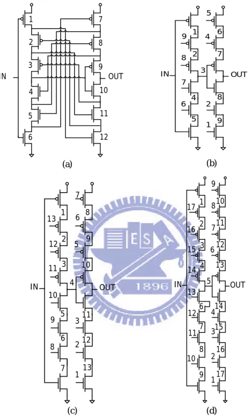
the larger propagation time and reduces the number of delay cells. For example, the level tree of enhanced IHDC uses cross lines to connect two double-cascode cells, as shown in Figure 5(a). In other words, the higher level enhanced IHDC is composed of plurality-cascode cells to increase longer delay time. The connected line between the two casecode cells is complex. We use a simple way to connect double-cascode cells or plurality-cascode cells. The connected lines combine the two cascade cells to use the net order by counting the net backwards as illustrated in Figure 5(b). The level four IHDC and the level five IHDC are shown in Figure 5(c) and (d), individually. The enhanced version of an IHDC still has the impermanent charge. The level 3 IHDC includes the bypass circuit type 1 as shown in Figure 6(a). The connected lines combine the two cascade cells to use the net order by counting the net interlaces as illustrated in Figure 6(b).
10 2 3 4 5 6 9 10 11 12 12 11 10 9 IN OUT 2 3 5 6 7 7 13 1 1 8 13 8 1 2 3 4 5 6 7 8 9 9 8 7 6 IN OUT 1 2 4 5 OUT 1 2 3 4 5 6 7 8 9 10 11 12 IN 3 4 5 6 7 12 13 14 15 12 11 10 IN OUT 3 4 6 7 8 8 16 2 2 11 13 9 1 10 14 9 17 1 15 16 17 (a) (b) (c) (d)
Figure 5 enhanced IHDC (a) level 3 (b) level 3 with numeral connection (c) level 4 (d) level 5
11
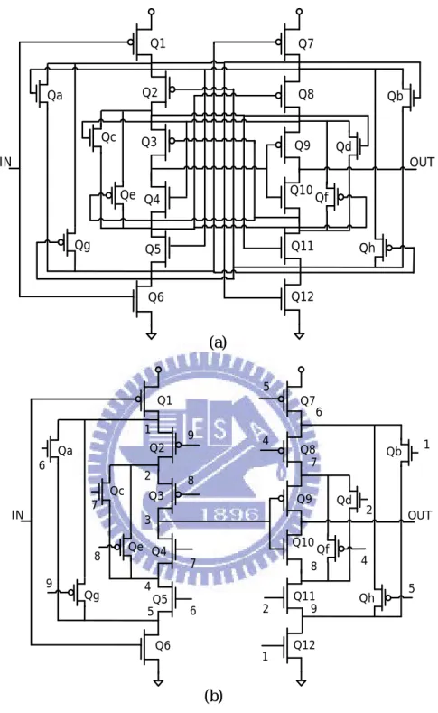
2.4 Characteristic of the IHDC
2.4.1 Background
In ADPLL applications, the propagation time and power consumption are important.
IN Q1 Q2 Q3 Q4 Q5 Q6 Q7 Q8 Q9 Q10 Q11 Q12 Qa Qc Qe Qg OUT Qb Qd Qf Qh (a)
Figure 6 level 3 IHDC includes the bypass circuit
IN Q1 Q2 Q3 Q4 Q5 Q6 Q7 Q8 Q9 Q10 Q11 Q12 Qa Qc Qe Qg OUT Qb Qd Qf Qh 1 2 3 4 5 6 7 8 9 1 1 5 5 9 9 2 2 4 4 7 7 8 8 6 6 (b)
12
The propagation time and power consumption of this delay cell is analyzed as follows: the propagation delay time is defined by the formula (1)
TP =(Tpr+T2 pf)……….. (1)
Tpf is the output fall time from the maximum level to the 50% voltage line, i.e.,
from VDD to (VDD /2); Tpr is the propagation rise time from the minimum level to the
50% voltage line, i.e., from 0V to (VDD /2).
Tpf = ln(2) τn………. (2)
Tpr= ln(2) τp………. (3)
Where the nMOS and pMOS time constant is defined by
τn = RnCout ….……….. (4)
τp = RpCout ………... (5)
Those time constants are due to the parasitic resistance and capacitances of the transistors.
The power consumption divides the currents into DC and dynamic (or switching) contribution. PDC is the DC term and Pdyn is due to dynamic switching events. When the
input voltage Vin is stable at a low potential, the nMOS is turned off. There is no direct current flow path between VDD and ground. When Vin is switched, small leakage currents exist in a realistic circuit. However, the leakage current is usually quite small, with a typical value on the order of a pico-ampere per gate. The dynamic power is calculated by the current during the charge or discharge event on the loading capacitor. The dynamic power dissipation is proportional to the signal frequency.
13
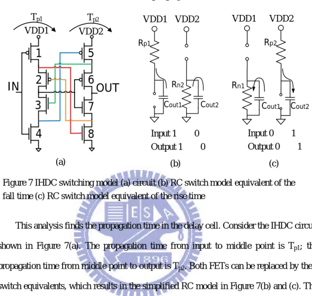
2.4.2 IHDC characteristics – the propagation time
This analysis finds the propagation time in the delay cell. Consider the IHDC circuit shown in Figure 7(a). The propagation time from input to middle point is Tp1; the
propagation time from middle point to output is Tp2. Both FETs can be replaced by their
switch equivalents, which results in the simplified RC model in Figure 7(b) and (c). The propagation time
Tp= Tp1+ Tp2 ……….………. (6)
This propagation time consists of a constant value, i.e., Resistor and Capacitor. A matching transfer is designed to have an equal parasitic resistance. In other words, the cell possesses the same value of the equivalent resistors. Combining these results, the propagation time is
Tp= ln(2) �Rp1Cout1+ Rn2Cout2+ Rn1Cout1+ Rp2Cout2�
= ln(2) [2R(Cout1+ Cout2)] ………..……… (7)
The equivalent resistors are proportional to the number of the stacking transistors; the loading capacitors are proportional to the number of the stacking transistors. Rearranging
Cout1 Cout2 Rp1 Rn2 Cout2 Cout1 Rp2 Rn1
IN
OUT
1
2
3
4
5
6
7
8
Figure 7 IHDC switching model (a) circuit (b) RC switch model equivalent of the fall time (c) RC switch model equivalent of the rise time
(a) (b) (c) Tp2 Tp1 VDD1 VDD2 VDD1 VDD2 VDD1 VDD2 Input 1 → 0 Output 1 → 0 Input 0 → 1 Output 0 → 1
14
the function to show the relation
Tp∝ (number of the stacking transistors)2 ……….…………. (8)
The propagation time is proportional to the square of the number of the stacking transistors.
2.4.3 IHDC characteristics – power consumption
The power consumption is usually divided into static (DC) and dynamic contributions.
P = PDC+ Pdyn ……….. (9)
The IHDC has a longer delay time and replaces many standard delay cells, leading to save the DC power. The dynamic power consumption is proportional to the signal frequency. The dynamic power reacts to a frequency. The frequency has the reciprocal of period. The period of the ring oscillator is the number n of the propagation delay cells. The circuit for finding the transient power dissipation illustrated in Figure 7.
Pdyn = f × VDD12× Cout1+ f × VDD22× Cout2
=n×2R(C 1
out1+Cout2)(VDD
2)(C
out1+ Cout2)
=�VDD2nR2� ……… (10)
The formula describes about the effect of the various elements on determining the level of a delay cell. The power consumption is proportional to the reciprocal of the number of cells.
P ∝(number of the stacking transistors)1 ……….……. (11)
2.4.4 Summary
The propagation time is proportional to the square of the number of the stacking transistors. The power consumption is proportional to the reciprocal of the number of cells. The number of the stacking transistors increases and the power consumption in the
15
condition of the same period time can be reduced.
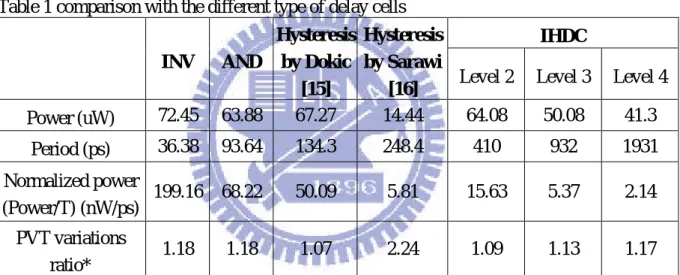
This chapter discusses the power consumption and the process-voltage-temperature (PVT) variations by comparing different types of the delay cells. The comparison of different delay cells simulated the total propagations time and power consumption, as shown in Table 1. There are different types of inverter, AND gate, Dokic type delay cell [15], Sarawi type delay cell [16] and the proposed delay cell from level 2 to level 4, as shown in Figure 8. The HDC has the lowest normalized power [2]. However, the PVT variations are the largest. The PVT variations increase the total frequency range to cover the operation frequency. As a result, the parameter of the PVT variations and normalized power influence the frequency range, cell number, power consumption and area. The normalized power of IHDC level 3 and level 4 is better than the HDC [2].
16
Table 1 comparison with the different type of delay cells INV AND Hysteresis by Dokic [15] Hysteresis by Sarawi [16] IHDC
Level 2 Level 3 Level 4 Power (uW) 72.45 63.88 67.27 14.44 64.08 50.08 41.3 Period (ps) 36.38 93.64 134.3 248.4 410 932 1931 Normalized power (Power/T) (nW/ps) 199.16 68.22 50.09 5.81 15.63 5.37 2.14 PVT variations ratio* 1.18 1.18 1.07 2.24 1.09 1.13 1.17
*PVT variations ratio = [(the period @SS corner) – (the period @FF corner)] ÷ (the period @TT corner)
Figure 8 different delay cells of (a) Inverter (b) AND gate (c) Dokic type HDC (d) Sarawi type HDC (e) IHDC - level 2
IN OUT IN OUT OUT
Q1 Q2 Q3 Q4 Q5 Q6 Q7 Q8 Qd Qa Qb Qc IN A B C D E D C A B (a) (b) (c) (d) (e)
17
3
Digitally controlled oscillator
3.1 Basic concepts of DCOs
The DCO is the key of the ADPLL module. Also, the most power consumption of a clocking circuit comes from the DCO. A DCO is the major bottleneck of an ADPLL in low power design. In other words, power reduction in a DCO design can effectively reduce the ADPLL system power, especially in low-power SoC applications.
We assume that the output waveform of the DCO is a square wave. The basic function of a DCO provides an output waveform which has a frequency of oscillation fDCO that is a function of a digital input word D as shown:
fDCO = f(D) = f(dn−12n−1+ dn−22n−2+ ⋯ + d121+ d020) ………. (12) The DCO transfer function is defined that the frequency fDCO is changed linearly with its
input word (D), as follows:
f(D) = fconstant+ D × ∆f ………..…… (13)
where fconstant is a constant frequency and ∆f is the frequency quantization step. Similarly,
a DCO transfer function that is linear in period is typically expressed as:
T(D) = 1 f(D)� = Tconstant+ D × ∆T ………..…… (14)
where Tconstant is constant offset period and ∆T is the period quantization step. In
addition, because the DCO period T(D) is a function of quantized digital input (D), the output range of the DCO is discontinuous. In other words, this result in the finite frequency step size ∆f and set some fundamental limits on the achievable jitter of the ADPLL. Therefore, the resolution of the DCO has to be sufficiently to meet acceptable jitter performance.
18
Generally, a ring oscillator is composed of odd number of inverters connected into a ring structure. The clock period of the ring oscillator is two times of the circular loop delay time. Different propagation delay time of the inverter produces different clock period. In addition, a variable number of inverters implement a variable delay. Therefore, there are two parameters to determine the clock period of the ring oscillator. One is the propagation delay time of a delay cell and another is the number of the delay cells. Based on these two parameters, the following many designs of the DCOs are presented.
A typical ring-oscillator consists of inverters in an ADPLL, as shown in Figure 9. The advantage is that the architecture is implemented by standard cells and simple designs. However, it can not change the output frequency. The output frequency is not fixed due to the PVT variations. In order to cope with PVT variations, a DCO adjusts to meet target frequency.
3.2.1
Linear architecture
Figure 10 shows a linear architecture [5]. The architecture uses an enable signal to control the output signal of the ring oscillator. The path selection consists of tri-state
Figure 9 a typical ring-oscillator
Enable Output
P4 P3 P2 P1
Figure 10 a linear architecture
19
inverters. The concept is that the modification delay path can adjust the output frequency of the DCO. The controlled codes of this architecture need an extra decoder from binary code change to one-hot code. The resolution of the DCO is poor due to the propagation time of one inverter. As a result, this architecture has a large area and a poor resolution.
3.2.2
Matrix tri-state architecture
The delay matrix of a DCO uses digital cells in the standard cell library, as shown in Figure 11 [7]. This architecture consists of several parallel tri-state inverters. The matrix of a DCO can adjust the output driving. The advantage has a fine resolution; the disadvantage is the large number delay cells, leading to a large area and huge power consumption.
3.2.3
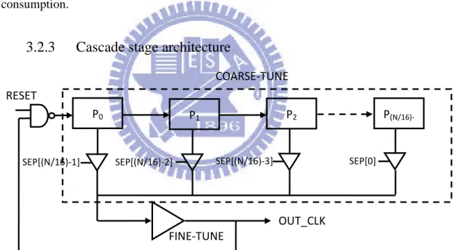
Cascade stage architecture
An improved DCO architecture is shown in Figure 12 [6]. The improved DCO is divided into two parts: a coarse-tuning stage and a fine-tuning stage. The coarse tuning stage provides the range of operation frequency. The fine tuning stage provides the resolution of the DCO. This architecture solves the poor resolution issue. A cascade-stage DCO provides high resolution, wide range and small number of delay cells
Figure 11 an improved DCO architecture
P (N/16)-RESET SEP[(N/16)-1] P0 P1 SEP[(N/16)-2] P2 SEP[(N/16)-3] SEP[0] FINE-TUNE OUT_CLK COARSE-TUNE
20
at the same time.
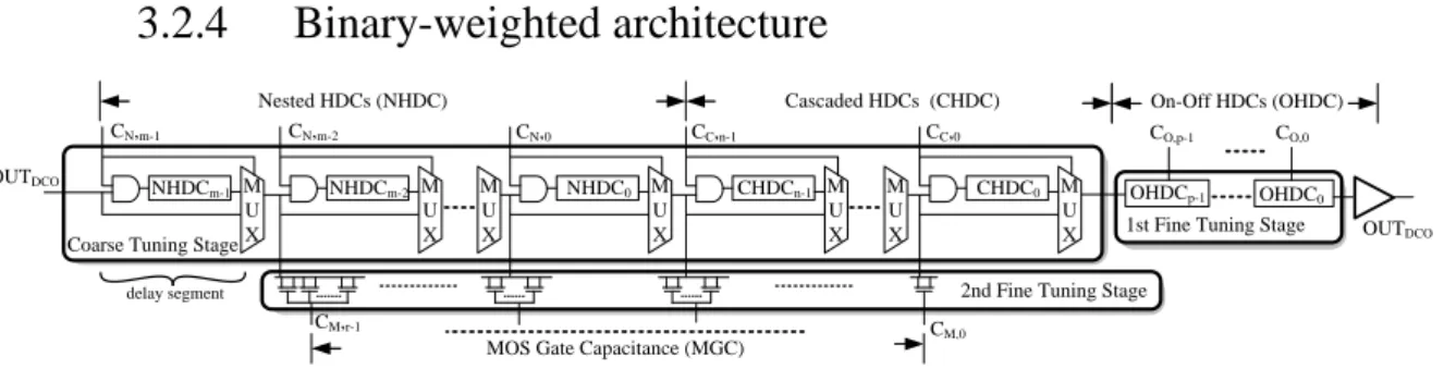
3.2.4
Binary-weighted architecture
A binary-weighted DCO architecture is shown in Figure 13 [2]. The control method in a coarse tuning stage is to choose a path by 2-input multiplexers for different propagation delay. In the fine tuning stages, it modifies the MOS gate capacitance by the digital control code. This architecture exempts the converter for binary codes to one-hot codes, which is typical in the linear DCO. However, the glitches are due to switching delay by a multiplexer. A binary-weighted architecture and a linear architecture both cause the glitch problem. Many path-selected circuits cause many glitches. As a result, the glitch of a binary-weighted DCO architecture is a serious problem. The glitch issue will be discussed in detail in the following chapter.
OUTDCO
Coarse Tuning Stage NHDCm-1 CN,m-1 M U X NHDCm-2 CN,m-2 M U X NHDC0 M U X M U X CN,0 CHDCn-1 M U X CC,n-1 M U X CHDC0 M U X CC,0 OHDCp-1 CO,p-1 CO,0 OUTDCO 1st Fine Tuning Stage
OHDC0
CM,r-1 C
M,0
2nd Fine Tuning Stage MOS Gate Capacitance (MGC)
Nested HDCs (NHDC) Cascaded HDCs (CHDC) On-Off HDCs (OHDC)
delay segment
21
Table 2 comparison table between the linear and binary-weighted architecture
Linear Binary weighted
Area Large Small
Power Large Small
Frequency limits High frequency Low frequency
Stability (code transition) Slight glitches Serious glitches
To analyze two types of ring oscillator architectures: linear and binary-weighted (BW) architecture as illustrated in Figure 14(a) and Figure 14(b). The comparison table is between the binary-weighted and the linear architecture in Table 2. The area and power of the binary-weighted architecture is smaller than a linear architecture. For example, a 12-bit DCO is implemented by the linear and the BW architectures respectively.
Area of a linear architecture = Multiplexer cells + Delay cells + Decoder = (2n × Tri-state buffer) + (2n-1 × one delay cell) + Decoder
= 4096 × Tri-state buffer + 4095 × one delay cell + Decoder ...… (15) Area of a BW architecture = Multiplexer cells + Delay cells
= (2n × Tri-state buffer) + (2n-1 × one delay cell)
= 24 × Tri-state buffer + 4095 × one delay cell ……….. (16) Figure 13 system block diagram of (a) the linear and (b) the binary-weighted
(a) (b) Delay 4096 Delay 2 Delay 1 RST code[1] code[0] code[11] Delay 4095 code[10]
Path Selection MUX RST Delay 4096 Delay 1 Decoder code[11:0] Delay 4095 Delay 2
22
The linear DCO only uses one bit to control one cell. The method of a linear architecture is not effective to control multi-path selector. Moreover, the linear DCO should build an extra decoder and larger number of tri-state buffer. As a result, the linear DCO area and power is larger than the binary-weighted DCO. The binary-weighted DCO can largely reduce the number of cells.
However, the fastest frequency of binary-weighted is limited. An example of a 12-bit DCO compares the linear architecture and the BW architecture.
Period of linear archiyecture = Tselect−path+ Treset+ D × ∆T
= 1 × TTri−state buffer+ 1 × TNAND+ D × ∆T………. (17)
Period of BW archiyecture = Tselect−path+ Treset+ D × ∆T
= 12 × TTri−state buffer+ 1 × TNAND+ D × ∆T ……. (18)
where Tselect-path and Treset is constant period, ∆T is period quantization step and D is the
function of a digital input word. The frequency of the DCO is composed of the fixed frequency and the controlled frequency. The fastest frequency of binary-weighted is limited by the fixed frequency. As a result, the binary-weighted architecture is suitable under the frequency of 1GHz.
3.2.5 Proposed architecture
Our proposed DCO uses the modified binary-weighted delay stage and the cascade-stage structure as illustrated in Figure 15(a) and (b) respectively. The modified binary-weighted delay stage creates a new path to shorten the fixed period, leading to increase the fastest frequency. It can reduce power consumption and area. The cascade-stage structure can achieve high resolution, wide range and small number of delay cells at the same time. Our proposed structure of the DCO can effectively use control code and largely reduce power consumption.
23
3.3 The proposed glitches solution
The glitches are due to switching delay by a multiplexer. Contingency pulses may be produced when the delay path changes. The contingency pulses always exist in the loop circuit. The glitch issue of a binary-weighted DCO is a serious problem. The ring oscillator must use delay cells to generate a clock signal and changes the delay in order to adjust the frequency. Figure 16 shows contingency pulses when the delay path changes. When the contingency pulses are happened, glitches in the loop circuit do not disappear.
Figure 14 block diagram of (a) the modified binary-weighted delay stage (b) the cascade-stage structure
1st COARSE TUNING 2nd COARSE TUNING 1st FINE TUNING 2nd FINE TUNING (b) (a) Delay x2n Delay x2 RST code[1] code[n] Delay x1 code[0] code[n-1] Delay x2(n-1)
24
The traditional method disables the clock output before changing the control code as shown in Figure 17 [8]. However, it causes the longer lock-in time and the intermittent output clock. The output clock is not continuous to degrade the jitter performance. The traditional solution cannot be applied in the precise clock system.
In order to analyze, a waveform divides a cycle into some segments. The analysis range discusses in a cycle after the codeword changes. First, we analyze that a 1-bit binary-weighted DCO has two cases: (i) the short delay path changes to the long delay path (Figure 18(a)) and (ii) the long delay path changes to the short delay path (Figure 19(a)). The short path passes though an AND gate and a MUX. The short period is composed of twice propagation by an AND gate and a MUX cell. The clock signal divides into 4 states by delay time as shown in Figure 18(b). Figure 18(c) is the process of analysis from short delay path to long delay path. In the same way, Figure 19(c) is the process of analysis from short delay path to long delay path. This is an enumeration method to analyze the time of the glitch occurrence. Therefore, the glitch cannot happen when the path changes from long delay to short delay. When codeword changes from short delay to long delay, the glitch will appear at
Figure 16 the traditional solution for glitches
DCO_CLK
code Code A Code B
Ref_CLK
ENABLE
Clock 1 Clock 2
code Code A Code B
glitch
25
(- TM) < Tchange < (0.5Tcycle - TM) ………. (19)
(a) (b)
(1) 0 < Tchang < (0.5Tcycle1 - TM) (2) (0.5Tcycle1 - TM) < Tchang < 0.5Tcycle1
: Glitch : No glitch
(3) 0.5Tcycle1 < Tchang < Tcycle1 – TM (4) (Tcycle1 – TM)< Tchang < Tcycle1
: No glitch : Glitch
(c)
Figure 17 from short delay path to long delay path: (a) circuits (b) waveform (c) analysis for changing codeword
26
If a 1-bit binary-weighted DCO expands to a 3-bit architecture, the glitch formula (19) can find the correct changing time of the code word. Figure 20 is an example of a 3-bits binary-weighted DCO. In this case, the circuits can change to the equivalent circuits. When code changes in the red block of Figure 20(c), the glitch will appear. The glitches do not happen at the falling edge of the DCO output signal. The proposed
(a) (b) 0 < Tchang < TP TP < Tchang < (0.5Tcycle1 – TM)
(0.5Tcycle1 - TM) < Tchang < 0.5Tcycle1 0.5Tcycle1 < Tchang < 0.5Tcycle1 + TP
0.5Tcycle1 + TP < Tchang < Tcycle1 - TM (Tcycle1 – TM)< Tchang < Tcycle1
(c)
Figure 18 from long delay path to short delay path: (a) circuits (b) waveform (c) analysis for changing codeword
27
solution is to use the synchronization cell (D Flip-flop) as shown in Figure 21. The proposed solution can find the correct changing timing to avoid glitches.
Figure 20 proposed solution for glitches (a) circuits (b) waveform
(a) (b) Delay cell Icode code 0 1 D Q OUT A B OUT Icode A B code 0 OUT 1 Icode 0 1 (a) (b)
Figure 19 a three bits binary-weighted DCO (a) circuits (b) equivalent circuits (c) waveform (c)
A
B
C
TP2 TM TNTP1TM TM TM Delay x4 Delay x1 RST code[0] code[2] Delay x2 code[1] Delay1 Delay2 RST Delay codeT
DT
P1T
M A B CT
P2T
N28
3.4 Structure of proposed DCO
Figure 22 shows the architecture of the proposed DCO. The proposed DCO is separated into four stages: 1st coarse-tuning stage, 2nd coarse-tuning stage, 1st fine-tuning stage and 2nd fine-tuning stage. The control method in the coarse tuning stages changes the propagation delay time by multiplexers (MUXs). The operation concept of the fine-tuning stage controls the output loading. The 1st coarse tuning stage is composed of the interlaced hysteresis delay cells (IHDCs), as shown in Figure 2. The IHDC uses two cascaded transistor chains with shared power current. Moreover, an IHDC is able to extend the propagation delay time and does not increase power consumption. In addition, the IHDC can avoid short-circuit current. Those cells can reduce power consumption of a DCO. The 2nd coarse tuning stage consists of the AND gates. In order to achieve better resolution and less power consumption, this coarse and fine tuning stage is divided into two different sub-stages. It should be noted that the controlled range of each stage is larger than the delay step of the previous stage. The cascade DCO structure does not have any dead zone larger than the LSB resolution of the DCO. Therefore, the delay time of the standard AND gate cell is smaller than the level 2 IHDC and larger than the series resistance and capacitance. The 1st fine tuning stage
RST
Code L,m Code L,m-1 Code L,0
Code A,n Code A,1 Code A,0 LV2
LVm-1 LVm
1st Coarse Tuning Stage
Code M,s Code M,s’ Code M,0
2n
Code RC,p
Code RC,p’ Code RC,1
Code C,q Code C,q’ Code C,1
2nd Coarse Tuning Stage
1st Fine Tuning Stage
2nd Fine Tuning Stage
DCO_OUT
29
consists of the equivalent resistor and capacitance, as shown in Figure 23. The transmission gate can be replaced by the equivalent resistance and the ideal switch. The series of the equivalent resistor and capacitance generate the output loading. The loading of the 1st fine tuning stage is larger than the loading capacitance of the 2nd fine tuning stage. The 2nd fine tuning stage consists of the MOS gate capacitance (MGC), as shown in Figure 24. The MOS gate capacitance (MGC) uses a logic code to change the output loadings for delay fine tunings. The delay cells of the 1st coarse tuning stage and the 2nd fine tuning stage have the largest and smallest delay step. The controlled range of the 1st coarse tuning stage need cover the operation range of the DCO. The propagation time of a delay cell determines the DCO resolution in the 2nd fine tuning stage. This architecture achieves the high resolution and the wide operation range at the same time. The proposed IHDC can provide larger delay step than the AND gate. The IHDC in the 1st coarse tuning stage replaces many the delay cells of the 2nd coarse tuning stage. The proposed IHDC can reduce the number of cells and save power consumption. The output period is composed of the fixed period and the variable period. The fixed period is equal to the Tconstant from Equation (14). The fixed period means that the smaller period and the fastest
frequency. The fixed period is the constant factor which comprises the propagation delay time of one NAND gate and many multiplexers. The fastest frequency is limited by the number of MUX. The proposed DCO creates a new path to shorten the fixed time, leading to increase the fastest frequency. In the proposed DCO architecture, the 4-input multiplexer generate a new short path to provide the faster output frequency.
30
3.5 Simulation results and layout
The proposed DCO is a four-tuning-stage ring oscillator with enable part as shown in Figure 25. The proposed DCO has total 14-bit resolution, including coarse tune and fine tune part. The IHDC stage is composed of the IHDC in the first coarse tuning stage. The AND stage is composed of the AND gate in the second coarse tuning stage. The second coarse tuning stage includes the binary weighted stage and the linear stage, leading to add a small decoder circuit. The TRMGC stage comprises the equivalent resistor of transmission gate and the MOS gate capacitance in the first fine tuning stage. The MGC stage is composed of the MOS gate capacitance in the second fine tuning stage. A main idea of the proposed DCO adjusts the different propagation delay time and the driving loading. The most significant advantage of many type delay cells is the low power
Figure 23 loading capacitance and resistance (a) the equivalent circuit (b) the proposed delay cell in 2nd fine tuning stage
(a) (b) Code In Out CI ΔC Code In Out
Figure 22 loading capacitance and resistance (a) the equivalent circuit (b) the proposed delay cell in 1st fine tuning stage
(a) (b) In Out Code R C In Out Code
31
consumption.
According to the methods in Section 2.2, 2.3 and 3.5, we propose the DCO architecture as Figure 22. The proposed DCO structure is designed and simulated using 90nm CMOS model. The simulation is in the best case, the typical case and the worst case. The simulation is the period of the DCO output clock versus the first coarse code, the second coarse code, the first fine code and the second fine code, as shown in Figure 26, Figure 27, Figure 28 and Figure 29 respectively. Tables 4, 5, 6 and 7 are the period of the DCO output period in each stage at tree corner cases.
Table 3 step and range of each tuning stage
1st Coarse Tuning 2nd Coarse Tuning 1st Fine Tuning 2nd Fine Tuning
Range (ps) 4350.18 1399.98 73.88 30.04
Step (ps) 525.16 103.69 24.63 4.29
Table 4 simulation result of the second fine tuning stage in the proposed DCO Delay (ps) fine code SS, 0.9V, 125℃ TT, 1V, 25℃ FF, 1.1V, -40℃ 00-000 1996.84 1053.02 656.54 00-001 2001.64 1056.9 672.36 00-010 2009.84 1062.02 675.46 00-011 2017.84 1065.88 678.48 00-100 2025.44 1070.6 681.94 00-101 2027.64 1074.72 685.08 00-110 2033.84 1078.94 688.06 00-111 2041.64 1083.06 691.02
Figure 24 proposed DCO block with the cascade stage RST 1st Coarse Tuning Stage 2nd Coarse Tuning Stage 1st Fine Tuning Stage 2nd Fine Tuning Stage
MGC
IHDC
AND
TR + MGC32
Figure 25 simulation of the DCO period versus the second fine code (a) SS corner: worst case; SS, 0.9V, 125℃
(b) TT corner: typical case; TT, 1.0V, 25℃
33
Table 5 simulation result of the first fine tuning stage in the proposed DCO Delay (ps) fine code SS, 0.9V, 125℃ TT, 1V, 25℃ FF, 1.1V, -40℃ 00-000 1996.84 1053.02 656.54 01-000 2039.44 1078 672.98 10-000 2085.04 1102.08 688.48 11-000 2130.04 1126.9 705.02
Figure 26 simulation of the DCO period versus the first fine code (a) SS corner: worst case; SS, 0.9V, 125℃
(b) TT corner: typical case; TT, 1.0V, 25℃
34
Table 6 simulation result of the second coarse tuning stage in the proposed DCO Delay (ps) coarse code SS, 0.9V, 125℃ TT, 1V, 25℃ FF, 1.1V, -40℃ 000-000000 1996.84 1053.02 656.54 000-001000 2189.80 1159.40 724.48 000-000001 2403.20 1266.94 788.68 000-010001 2580.40 1365.16 852.42 000-000011 2822.60 1492.14 927.24 000-100011 2999.80 1590.22 991.10 000-000111 3264.80 1727.08 1073.76 000-001111 3467.80 1838.10 1142.46 000-010111 3647.20 1932.66 1203.50 000-011111 3846.60 2043.20 1275.04 000-100111 4018.00 2139.80 1336.64 000-101111 4220.20 2249.00 1405.62 000-110111 4396.40 2344.60 1466.34 000-111111 4599.20 2453.00 1535.62
35
Table 7 simulation result of the first coarse tuning stage in the proposed DCO Delay (ps) coarse code SS, 0.9V, 125℃ TT, 1V, 25℃ FF, 1.1V, -40℃ 000-000111 3264.80 1727.08 1073.76 001-000111 4252.60 2256.00 1404.66 010-000111 5241.00 2784.40 1727.18 011-000111 6248.80 3314.00 2058.00 100-000111 7212.20 3809.80 2345.20 101-000111 8204.20 4347.20 2680.20 110-000111 9202.00 4871.60 3004.20 111-000111 10191.40 5403.20 3335.20
36
The operational frequencies responses to the process, temperature and voltage variations are shown in Figure 26, Figure 27, Figure 28, Figure 29 and Figure 30. The curves have a good linearity which is a key factor of ADPLL performance. The range of each stage is larger than the step of the preceding stage. As shown in Figure 30, the output frequency range covers from 265 to 500MHz in three corner cases.
Table 8 lists comparison results with the state-of-the-art DCOs. The hysteresis delay cell type DCO [2] based on Schmitt cells uses the hysteresis phenomena. This architecture applies in low power system. However, the HDC has large the PVT variations. In order to Figure 29 simulation of the DCO period of coarse code and fine code in PVT variations
Figure 30 layout of the proposed DCO
10.25μm 50μm
37
cover the PVT variations, this architecture needs a larger number of delay cells than the proposed DCO architecture. The standard cell type of the DCO [12] is a general architecture. The voltage-controlled oscillator [17] can also achieve high jitter performance. However, an amplifier needs a large area. In terms of power consumption and area, the proposed DCO has the lowest power consumption and the smallest area. This architecture does not need special algorithm to control DCO. We can use a sample controller to dominate the DCO output frequency. As a result, the benefits of the proposed DCO are low power consumption, small area, wide operation range and linear frequency.
Table 8 comparison with existing DCOs
Proposed TCAS II 2010 [2] TCAS II 2007 [12] ISSCC 2008 [17] Technology 90nm 90nm 90nm 65nm Supply Voltage (V) 1 1 1 1.2 Frequency (MHz) 170~949.6 3.8~163.2 191~952 12 Power consumption 128 uW @480MHz 5.4 uW @3.4MHz 140 uW @200MHz 9uW @12MHz
Area (um2) 512.5 6400 N/A 30000
Output jitter (RMS) 1 ps @480MHz (0.05%) 49.3 ps @5MHz (0.02%) 8.18 ps @417MHz (0.34%) -109dBc/Hz @12MHz (0.01%)
38
4
Chip Implementation
4.1 Architecture of the ADPLL
Figure 32 shows the proposed ADPLL block diagram. The ADPLL basic blocks contain a phase / frequency detector (PFD), a controller, a digitally controlled oscillator (DCO) and a frequency divider. The operation procedure of the proposed ADPLL is as follows. The output frequency of the DCO sends into divider and feedbacks signal to the PFD. The PFD detects the phase different between reference clock and feedback clock. Then, the PFD generates a signal “lead” or “lag” to the controller. The controller generates proper codes to DCO depending on the signal “lead” or “lag”.
D Q D Q D Q D Q D Q D Q Y0 Y1 Y2 Y5 Y4 Y3 Code 8 Code 9 Code 11 Code 12 Code 13 PFD Controller Divider REF_CLK FB_CLK lead lag Code 13~5 Code 4~0 Coarse tuning Control code Fine tuning Control code DCO
Glitch cancellation device
12MHz 480MHz RST LV2 LV3 LV4 22 Code 4 Code 3 Code 2 Code 1 Code 0 DCO_OUT Y5 Y4 Y3 Y2 Y1 Y0 Code 10 D Q D Q D Q Y0 Y2 Y4 Code 6 Code 7 Code 5
39
4.1.1 Phase / Frequency Detector
The PFD architecture is shown in Figure 33[6]. When the feedback clock leads the reference clock, the signal “lag” presents a low level and the signal “lead” keep high. On the contrary, when the feedback clock lags the reference clock, the signal “lag” presents a low and the signal “lead” keeps high. The ADPLL controller changes code word to DCO depend on PFD signal.
Figure 34 shows the simulation result of the PFD. The simulation sweeps the phase error from the feedback clock leading the reference clock for 30ps to feedback clock
Figure 32 modified 3-state PFD architecture
D
SETQ
RSTD
SETQ
D
RSTQ
Digital Pulse Amp.D
RSTQ
Ref_CLK Ref_CLK FB_CLK lead lag FB_CLK QU QD BU BD RST RST Digital Pulse Amp.Figure 33 simulation result of the PFD circuit Ref_CLK FB_CLK lead lag 0 30ns 30ps 20ps 10ps -10ps -20ps -30ps Phase error 0ps
40
lagging reference clock for 30ps. The dead zone of PFD is around 10ps.
4.1.2 Control unit
The process divides into two operation modes: frequency searching mode and phase tracking mode. Phase acquisition mode starts when the frequency acquisition mode finishes. When the ADPLL controller receives the signal “lead” and “lag” from the PFD and changes the DCO control code. The control algorithm uses the binary searching [14]. The output frequency starts at the middle operating range of the DCO and the search step is one fourth of the operating range at the beginning. The search step will be reduced to one half of pervious step. The frequency searching mode completes when the search step reduce to one. Finally, the DCO control code converges to a target frequency.
4.2 Summary
The ADPLL core circuit layout is shown in Figure 35. This chip is fabricated in UMC 90nm 1P9M standard CMOS process. The chip size is 115 x 75um2. The simulation result of the ADPLL is shown in Figure 36. The frequency of reference clock is 12MHz, and the division ratio is 40. The frequency of the ADPLL output clock is 480MHz (= 12MHz x 40). The power consumption of the ADPLL is 271uW (@480MHz, 1.0V). The peak-to-peak jitter at 480MHz is 80ps. The proposed ADPLL using binary search algorithm is proposed to achieve locking within 42 cycles.
41
Table 9 performance summary of the proposed ADPLL Proposed ADPLL Technology 90nm Supply Voltage 1V Reference clock 12 MHz Output Frequency 480 MHz Power consumption 271 uW @480MHz
Area 115um x 75um
Output jitter (pk-pk) 80 ps @480MHz Figure 34 layout of the proposed ADPLL
DCO
PFD
Controller & Divider
75μm
115μm
42
5
Conclusion
5.1 Conclusion
A DCO is a key component of the ADPLL. The DCO affects the performance of an overall ADPLL and occupies the major part of power consumption in an ADPLL. In this thesis, the structure of the proposed DCO mixes a modified binary-weighted delay stage and a cascade-stage structure. The proposed DCO can reduce power consumption. However, the disadvantage of the binary-weighted structure is the serious glitches. The glitches are due to switching delays. One multiplexer generates one glitch. The binary-weighted DCO uses a lot of multiplexers and the glitch issue becomes more serious. The proposed solution with the synchronization cell eliminates the occurrence of glitches. The proposed DCO can effectively reduce power consumption. The coarse tuning stage utilizes AND gates to disable the unused delay cells and reduces redundant power. By using the IHDC, it can replace many delay cells of the second coarse tuning stage. This architecture can reduce the number of cells and save power consumption. The fine tuning stage adjusts output loading and utilizes the transistor resistance and capacitance. A modified stage multiplexer type DCO with 14-bit control code is realized to cover a wide operating range from 170MHz to 949MHz. The power consumption of proposed IHDC is reduced over 87% compared to that from AND gates of UMC 90nm standard cell library.. The power consumption of the proposed DCO is 128uW. A design example of an ADPLL is implemented in UMC 90nm 1P9M standard CMOS process. The core size is 115 x 75 um2. The power consumption of the post-layout simulation is 271uW at input 12MHz frequency and output 480MHz frequency.
43
Reference
[1] T. Tokairin, M. Okada, M. Kitsunezuka, T. Maeda, and M. Fukaishi, "A 2.1-to-2.8GHz All-Digital Frequency Synthesizer with a Time-Windowed TDC,” IEEE International
Solid-State Circuits Conference, pp. 516-517, 2010
[2] M.C. Chen, J.Y. Yu, and C.Y. Lee, “A Sub-100μW Area-Efficient Digitally-Controlled Oscillator Based on Hysteresis Delay Cell Topologies,” IEEE Asian Solid-State Circuits
Conference, Nov. 2009
[3] J. Dunning, J. Lundberg, and E. Nuckolls, “An All Digital Phase Locked Loop with 50-cycle Lock Time Suitable for High Performance Microprocessors,” IEEE journal of
Solid-State Circuits, vol.30, no.4, pp. 412-422, Apr. 1995
[4] J.Y. Yu, J.T. Chen, M.H. Yang, C.C. Chung, and C.Y. Lee, “An All-Digital Phase-Frequency Tunable Clock Generator for Wireless OFDM Communications Systems,”
IEEE International SOC Conference, pp. 305-308, Sep. 2007
[5] Chi-Cheng Cheng, “The Analysis and Design of All-Digital Phase-Locked Loop (ADPLL),” M.S. Dissertation, Department of Electronics Engineering, National Chiao Tung University, Taiwan, Jul. 2001.
[6] C.C. Chung, and C.Y. Lee, “An All Digital Phase-Locked Loop for High-Speed Clock Generation,” IEEE journal of Solid-State Circuits, vol. 38, no. 2, pp. 347-351, Feb. 2003
44
[7] Thomas Olsson, “A Digitally Controlled PLL for SoC Application,” IEEE Journal of
Solid-State Circuits, vol. 39, no. 5, pp. 751-759, May 2004
[8] C.C Wang, C.C. Huang and S.L Tseng, “A Low-Power ADPLL Using Feedback DCO Quarterly Disabled in Time Domain,” Microelectronics Journal, vol. 39, pp. 832-840, May 2008
[9] T.Y. Hsu, and C.Y. Lee, “An All-Digital Phase-Locked Loop (ADPLL)-Based Clock Recovery Circuit,” IEEE Journal of Solid State Circuits, vol. 34, no.8, pp.1063-1073, Aug. 1999
[10] T.Y. Hsu, C.C. Wang, and C.Y. Lee “Design and Analysis of a Portable High-Speed Clock Generator,” IEEE Transactions on Circuits and System II, Analog and Digital
Signal Processing, vol. 36, no. 10, pp. 1574-1581, Oct. 2001
[11] T. Olsson, and P. Nilsson, “A Digitally Controlled PLL for SoC Applications,” IEEE
Journal of Solid-State Circuits, vol. 39, no. 5, pp. 751-760, May 2004
[12] D. Sheng, C.C. Chung, C.Y. Lee, “An Ultra-Low-Power and Portable Digitally Controlled Oscillator for SoC Application,” IEEE Transactions on Circuits and Systems II, vol. 54, pp. 954-958, Nov. 2007
[13] P.L. Chen, C.C. Chung, and C.Y. Lee, “A Portable Digitally Controlled Oscillator Using Novel Varactors,” IEEE Transactions on Circuits and Systems II, vol. 52, pp. 233-237, May 2005
45
[14] D. Sheng, C.C. Chung, and C.Y. Lee, “An All-Digital Phase-Locked Loop with High-Resolution for SoC Application,” International Symposium on VLSI Design
Automation and Test, pp. 1-4, Apr. 2006
[15] B.L. Dokic, “CMOS NAND and NOR Schmitt Circuits,” Microelectronics Journal, vol. 27, no. 8, pp. 757-765, 1996
[16] S.F. A1-Sarawi, “Low Power Schmitt Trigger Circuits,” Electron Letter, vol. 38, no. 18, pp. 1009-1010, Aug. 2002
[17] P. F. J. Geraedts, E. van Tuijl, E. A. M. Klumperink, G. J. M. Wienk, and B. Nauta, “A 90 μW12MHz Relaxation Oscillator with A -162 dB FOM,” in Proc. IEEE ISSCC Dig.
Tech. Papers, pp. 348-350, Feb. 2008
[18] John P. Uvemura, “Introduction to VLSI Circuits and system,” Jul. 2002
[19] H.T. Ahn, and D.J. Allstot, “A Low-jitter 1.9V CMOS PLL for UltraSPARC Microprocessor Applications,” IEEE Journal of Solid State Circuits, vol. 35, no. 3, Mar. 2000
[20] C.C. Huang, and S.I. Liu, “A Leakage-Suppression Technique for Phase-Locked Systems in 65nm CMOS,” IEEE International Solid State Circuits Conference, pp. 400-401, Feb. 2009
![Figure 10 shows a linear architecture [5]. The architecture uses an enable signal to control the output signal of the ring oscillator](https://thumb-ap.123doks.com/thumbv2/9libinfo/8225322.170712/28.892.150.803.419.1037/figure-linear-architecture-architecture-enable-signal-control-oscillator.webp)
![[2015-Fall] WNFA lab1 - CamCom](data:image/gif;base64,R0lGODlhAQABAIAAAP///wAAACH5BAEAAAAALAAAAAABAAEAAAICRAEAOw==)