國 立 交 通 大 學
電 子 工 程 學 系 電 子 研 究 所
碩 士 論 文
奈米碳管於場發射元件之應用
Study on Carbon Nanotubes for Field
Emission Devices Applications
研 究 生:謝 振 宇
指導教授:鄭 晃 忠 教授
奈米碳管於場發射元件之應用
Study on Carbon Nanotubes for
Field Emission Devices Applications
研 究 生:謝振宇 Student: Chen-Yu Hsieh
指導教授:鄭晃忠 博士 Advisor: Dr. Huang-Chung Cheng
國 立 交 通 大 學
電子工程學系 電子研究所碩士班
碩士論文
A Thesis
Submitted to Institute of Electronics
College of Electrical Engineering and Computer Science National Chiao Tung University
In Partial Fulfillment of the Requirements For the Degree of
Master of Science in
Electronic Engineering June 2004
Hsinchu Taiwan Republic of China
奈米碳管於場發射元件之應用
研究生: 謝振宇 指導教授: 鄭晃忠 博士
國立交通大學電子工程學系 電子研究所碩士班
摘 要
本論文主要針對場發射材料與元件結構為主題作深入探討。在場發
射材料的合成部分,我們利用微波電漿輔助化學氣相沉積系統,藉由控
制催化層厚度來成長不同形態的奈米碳管。此外,由場發射測試中可以
發現,奈米碳管具有非常優異的場發射特性,而密度較高的奈米碳管因
為電場之遮蔽效應(screening effect)使得其場發射特性並不因其具有較
高密度之場發射源而變好。為了進一步改善奈米碳管之場發射特性,我
們亦提出了利用高密度電漿處理來改變奈米碳管之密度以降低電場之
遮蔽效應,實驗結果證實在適當的條件之下,奈米碳管之場發射起始電
場(由
0.9 V/µm 下降至 0.19 V/µm)可以大幅降低,而場發射電流亦可
大幅增加(上升至 15 mA/cm
2操作於 0.8 V/µm時)。
除了利用電漿後處理的方式,我們藉著遮蔽效應,在過密碳管中只
有邊緣的部分易於發射電子的觀念,設計不同大小的方形矩陣來增加總
邊長的方式,有效增加發射源面積,以達到降低起使電壓的目的。同時,
利用此法,更可以節省碳管後處理的製程步驟,節省時間以及節省成本。
為了符合場發射顯示器低電壓操作的目的,我們利用一控制閘極來
製造奈米碳管之場發射三極元件,我們以半導體製程技術縮小了元件的
尺寸,並利用選擇性成長奈米碳管的技術,以控制奈米碳管成長長度的
方式來製作場發射三極元件,為了有效降低閘極電流,使射出電子能有
效到達陽極,以增加亮度顯示,及避免碳管過長,其與閘極接觸而產生
短路現象。我們提出閘極上絕緣層三極結構來克服上述問題。同時順利
地將閘極操作電壓降低到 18 伏特;達到低壓操作及低漏流的目的。
Study on Carbon Nanotubes on Field
Emission Devices
Student : Chen-Yu Hsieh Advisor : Dr. Huang-Chung Cheng
Department of Electronic Engineering &
Institute of Electronics
National Chiao Tung University
Abstract
Field emission materials and devices are synthesized and fabricated in this thesis. For the synthesis of field emission materials, carbon nanotubes (CNTs) with various morphologies have been synthesized using microwave plasma-enhanced chemical vapor deposition (MPECVD) by controlling the thickness of the catalyst film. The fabricated CNTs emission arrays showed excellent field emission properties, however, the field emission properties of the high density CNTs degraded for the screening effect of the electric field. To improve the field emission properties of the CNTs, a post treatment process via plasma was proposed. The results depicted the field emission properties can be upgraded with proper plasma post treatment conditions.
Besides the plasma post treatment, we make use of the concept of screening effect that only the CNTs on the edge of the densely grown area could be easily emitted the electrons. The different pattern dimension arrays were applied to increase the total length.
The increase of length means the raise of emitting area. The great improvement of turn-on field were achieved. At the same time, we could improve the electrical characteristics without extra process like plasma post treatment and cost down.
The CNTs triode structures with an extraction gate were proposed to achieve the low voltage modulation. CNTs triodes with reduced gate diameter were fabricated by the semiconductor fabrication process and the selective growth of CNTs with controlled length. To lower the gate current effectively and avoid the short circuit problem between gate and emitters, we proposed an insulated gate structure field emission triode. The turn-on gate voltage was 18 V. It has successfully reduced the gate leakage current and the short circuit problem between gate and emitters to improve the field emission characteristics.
誌 謝
謹以此論文,獻給我的父母,謝文榮先生與陳華玉女士,感謝他
們多年來的培育,不僅這兩年,更為了一直以來他們不求回報的支持
與付出,使我能有今日的成就。
接著,要感謝在國立交通大學與清華大學數年來所有教導過我的
老師,尤其是我的指導教授鄭晃忠博士。他們對研究的積極專注以及
實事求是的態度,深深影響著學生。謝謝他們在論文研究和為人處世
方面的指導與鼓勵,才能順利地完成學位。
其次,要感謝交通大學奈米中心和國家奈米元件實驗室提供完善
的實驗設備,並在實驗設備及維護上給予最大的支持與配合,使研究
得以順利完成。
感謝學長在實驗啟蒙階段對我的許多訓練,以及實驗室同學、學
弟的關心以及幫助。認識的時間兩年也許太短,一年實是不長,能與
大家共事是一種幸運的緣分。
感謝我的朋友,在這兩年中陪我走過我的不安、徬徨、憂愁、失
落,與我分享我的驕傲、快樂、心得、成就。
諸位口試委員熱心的建議與指導,使得視野更加寬廣,在此一併
致謝。
Contents
ABSTRACT(Chinese)..………...………..……….….……i ABSTRACT...……….……….iii ACKNOWLEDGEMENT……….……….………..v CONTENTS……….………vi TABLE LISTS……….……….…..viiiFIGURE CAPTIONS ……….………ix
CHAPTER 1 Introduction 1.1 History of Vacuum Microelectronics……….……...………1
1.1.1 Overview of Vacuum Microelectronics………..…….1
1.1.2 Theory Background………...……. 3
1.2 Applications of Vacuum Microelectronic Devices………...6
1.2.1 Vacuum Microelectronic Devices for Electronic Circuits………...…7
1.2.2 Field Emission Displays………...…...8
1.3 Recent Developments of Field Emission Devices for Field Emission Displays……...9
1.3.1 Cathode Structures and Materials for Field Emission Displays.……….…..10
1.3.1.A Spindt-Type Field Emitters………...10
1.3.1.B Si Tip Field Emitters………..11
1.3.1.C Carbon and Nano-Sized Emitters………...……....11
1.4 Motivation………...…..13
1.5 Thesis Organization………...………...………..14
High-Density-Plasma Post Treatment and Pattern Dimension ……...…...16
2.1 Introduction ……….... 16
2.2 Experimental Procedures………...18
2.2.1 MPECVD Process………...………… 18
2.2.2Inductively Coupled Plasma (ICP) Process……….……….19
2.2.3 Measurement System for Vacuum Microelectronic Devices…………...……….20
2.3 Results and Discussions………..…….… 21
2.3.1The Effect of Plasma Post Treatment………….………...….……..21
2.3.2The Effect of Pattern Dimension……….….….. .23
2.4 Summary and Discussions……….….…..24
CHAPTER 3 Fabrication and Characterization of Insulated Gate Structure Field Emission Device Based on Carbon Nanotubes………....….……... 25
3.1 Introduction……….….….25
3.2 Experimental Procedures……….……. 27
3.3 Results & Discussions……….….….28
3.3.1 Comparison Electrical Characteristics between Conventional and Insulated Gate Structure Triode……….…..….28
3.3.2 Gate Leakage in Conventional and Insulated Gate Structure Triode……….…..29
3.3.3 Field Emission Stability……….…...30
3.4 Summary……….….……..30
CHAPTER 4 Conclusions and Future Prospects………..…….….…32
References………...….…35
Table Lists
Chapter 1
Table 1-1 Comparison between vacuum microelectronics and solid-state electronics.
Chapter 2
Table 2-1 Parameters of different plasma post treatments.
FIGURE CAPTIONS
Chapter 1
Fig. 1-1 Energy diagrams of vacuum-metal boundary: (a)without external electric field; and (b) with an external electric field.
Fig. 1-2 The schematic diagram of (a) conventional CRT, (b) FED.
Fig. 1-3 The SEM micrograph of (a)Spindt type triodes array, (b) Spindt type field emission triode.
Fig. 1-4 The FED products based on Spindt type field emitters, (a) motorola 5.6” color FED, (b) Pixtech 5.6” color FED,(c) Futaba 7” color FED and (d)
Sony/Candescent 13.2” color FED.
Fig. 1-5 (a) Si tip formed by isotropic etching and (b) Si tip field emission triodes array formed by CMP.
Fig. 1-6 (a) SEM image of CNT cathode from Samsung’s FED. (b) Demonstration of a 4.5-inch FED from Samsung. The emitting image of fully sealed SWNT-FED at color mode with red, green, and blue phosphor columns.
Chapter 2
Fig. 2-1 The relationship of current density and distances between emitters.
Fig. 2-2 Microwave Plasma Enhanced Chemical Vapor Deposition (MPECVD) system. Fig. 2-3 Growth mechanism of carbon nanotubes by MPECVD.
Fig. 2-4 SEM micrographs of the tip-growth mode of CNTs by MPECVD. Fig. 2-5 Procedures of CNTs treated with plasma post treatments.
Fig. 2-6 High vacuum measurement system.
Fig. 2-8 (a)Vertically aligned and high density of nanotubes (b)Diameter distribution of carbon nanotubes.
Fig. 2-9 Plasma post treatment (a)Non-PPT (b)200W,60s (c)300W,60s (d)400W,60s. Fig. 2-10 Cross section (a)Non-PPT (b)200W,60s (c)300W,60s (d)400W,60s.
Fig. 2-11 (a)J-E curve (b)F-N plot of different treatment time.
Fig. 2-12 Plasma post treatment (a)300W,30s (b)300W,60s (c)300W,90s. Fig. 2-13 Cross section (a)300W,30s (b)300W,60s (c)300W,90s.
Fig. 2-14 (a)J-E curve (b)F-N plot of different treatment time at 300W. Fig. 2-15 Plasma post treatment (a)200W,30s (b)200W,60s (c)200W,90s. Fig. 2-16 Plasma post treatment (a)400W,30s (b)400W,60s (c)400W,90s. Fig. 2-17 J-E curve of all treatment conditions.
Fig. 2-18 Simulation of screening effect.
Fig. 2-19 Pattern dimension (a)1000 µm(b)100 µm(c)10 µm.
Fig. 2-20 (a)J-E curve and (b)F-N plot of different pattern dimension.
Chapter 3
Fig. 3-1 Fabrication procedure of the carbon nanotubes insulated gate structure field emission device.
Fig. 3-2 (a)SEM of conventional triode (b)short circuit problem between gate and emitters. Fig. 3-3 Gate voltage versus (a)anode current (b)gate current in triode structure.
Fig. 3-4 SEM of insulated gate structure field emission triode (a)top view (b)cross section. Fig. 3-5 (a) The field emission current versus gate voltage, the anode was set at 450 volt, (b)
The F-N plot of the fabricated device, the linearity clarifies the field emission phenomenon.
Fig. 3-6 The field emission current versus anode voltage with different gate bias. Fig. 3-7 Gate voltage versus gate leakage current.
Fig. 3-8 Emission current stability of the insulated gate structure CNTs triode over a period of 1500 seconds.
Chapter 1
Introduction
1.1 History of Vacuum Microelectronics
1.1.1 Overview of vacuum microelectronics
Vacuum tubes have been gradually replaced by solid state electronic devices since the invention of solid state transistors in the late 1940s for the tiny volume, low cost, better reliability, and more power efficiency of solid state devices. For the past decades, great improvements on semiconductor manufacturing technology gave a new life to vacuum electronics for the professional micro fabrication process to fabricate tiny vacuum devices, which is now called vacuum microelectronics. “Vacuum state” devices have a great deal of superior advantages as compared with solid-state devices, including fast carrier drift velocity, radiation hardness, and temperature insensitivity. For example, the saturation drift velocity is limited to less than 3×107 cm/s in all semiconductor due to
scattering mechanism whereas the saturation drift velocity in vacuum is limited theoretically to 3×1010 cm/s and practically to about 6-9×108 cm/s [1.1]. Moreover,
temporary or permanent radiation effect is negligible in vacuum devices for no medium being damaged. Additionally, the effect of temperature on performance is reduced in vacuum devices simply for no medium causing the temperature effect in semiconductor,
such as increased lattice scattering or bulk carrier generation/recombination. Table 1-1 shows the comparison between vacuum microelectronic and semiconductor devices.
Recent developments in vacuum microelectronics started in 1928, when R. H. Fowler and L. W. Nordheim published the first theory of electron field emission from metals using quantum mechanics [1.2]. This theory is contrary to thermionic emission, which metal has to be heated so that some of the electrons in the metal gain enough thermal energy to overcome the metal/vacuum barrier; according to the Fowler-Nordheim theory, an applied electric field of approximately 103 V/µm is needed for electrons to tunnel through the sufficiently narrow barrier [1.2]. To reach the high field at reasonable applied voltage, producing the field emitters into protruding objects is essential to take advantage of field enhancement. It was not until 1968 when C. A. Spindt camp up with a fabrication method to create very small dimension metal cones that vacuum microelectronic triodes became possible [1.3]. From the late 1960s to the year 1990, Ivor Brodie, Henry F. Gray, and C. A. Spindt made many contributions in this field. Also, most of research was focused on the devices similar to the Spindt cathode during the past three decades.
In 1991, a group of research of the French company LETI CHEN reported a microtip display at the fourth International Vacuum Microelectronics Conference [1.4]. Their display was the first announcement of a practical vacuum microelectronic device. From then on, a great amount of researchers all over the world are devoted themselves to this interesting, challenging, and inventive field. Part of the work focused on fabricating very small radius silicon tip by utilizing modern VLSI technology [1.5-1.6]. Some of them increased the emission current by coating different metals, such as W, Mo, Ta, Pt etc.,
even diamond on field emission arrays [1.7-1.9]. Different device schemes also have been proposed to enhance the emission current density, stability, and reliability.
1.1.2 Theory Background
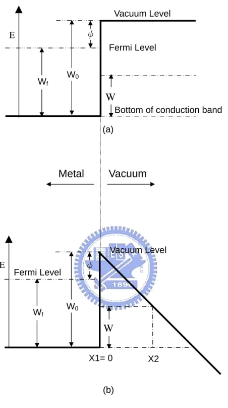
Electron field emission is a quantum mechanical tunneling phenomenon of electrons extracted from the conductive solid surface, such as a metal or a semiconductor, where the surface electric field is extremely high. If a sufficient electric field is applied on the emitter surface, electrons will be emitting through the surface potential barrier into vacuum, even under a very low temperature. In contrast, thermionic emission is the hot electron emission under high temperature and low electric field. Fig. 1-1(a) demonstrates the band diagram of a metal-vacuum system.
Here W0 is the energy difference between an electron at rest outside the metal and
an electron at rest inside the metal, whereas Wf is the energy difference between the
Fermi level and the bottom of the conduction band. The work function φ is defined as φ = W0 - Wf. If an external bias is applied, vacuum energy level is reduced and the potential
barrier at the surface becomes thinner as shown in Fig. 1-1(b). Then, an electron having energy “W” has a finite probability of tunneling through the surface barrier. Fowler and Nordheim derive the famous F-N equation (1.1) as follow [1.2]:
( )
exp[ 2 ( )/ ] 3 2 2 E y v b y t aE J φ φ − = , (1-1)where J is the current density (A/cm2). E is the applied electric field (V/cm), φ is the work function (in eV), a = 1.56×10⁻⁶, b = -6.831×10⁻⁷, y = 3.79x10-4×10-4E1/2/φ, t2(y)~1.1
and v(y) can be approximated as [1.10] v(y)=cos(0.5πy), (1-2) or ( ) 0.95 2. (1-3) y y v = −
Typically, the field emission current I is measured as a function of the applied voltage V. Substituting relationships of J = I/α and E = βV into Eq.(1-1), where α is the emitting area and β is the local field enhancement factor of the emitting surface, the following equation can be obtained
exp[ ( ) ] ) ( 2 3 2 2 2 V y bv y t V A I β φ φ αβ − = . (1-4)
Then taking the log. form of Eq. (1-4) and v(y) ~ 1
] 2.97 10 ( ( )) ) ( 10 54 . 1 log[ ) log( 2 3 7 2 2 6 2 V y v y t V I β φ φ αβ × − × = − , (1-5)
from Eq. (1-5), the slope of a Fowler-Nordheim (F-N) plot is given by
2.97 10 ( 2) 3 7 β φ × = ≡slopeFN S , (1-6)
The parameter β can be evaluated from the slope S of the measured F-N plot if the work function φ was known
2.97 10 ( 2) 3 7 S φ β =− × (cm-1), (1-7)
The emission area α can be subsequently extracted from a rearrangement of Eq. (1-5) exp( 9.89)exp(6.53 10 ) 10 4 . 1 ) ( 2 3 7 2 6 2 V V I β φ φ β φ α − × × = − (cm2). (1-8)
For example, the electric field at the surface of a spherical emitter of radius r concentric with a spherical anode (or gate) of radius r+d can be represented analytically by
( ) d d r r V E= + , (1-9)
Though a realistic electric field in the emitter tip is more complicated than above equation, we can multiply Eq.(1-9) by a geometric factor β` to approximate the real condition. Etip ≡function of (r,d) =β` ( ) d d r r V + , (1-10)
where r is the tip radius of emitter tip, d is the emitter-anode(gate) distance and β` is a geometric correction factor [1.11].
For a very sharp conical tip emitter, where d >> r, Etip approaches to β`(V/r). And
for r>>d, Etip approaches to β`(V/d) which is the solution for a parallel-plate capacitor
and for a diode operation in a small anode-to-cathode spacing.
As the gated FEA with very sharp tip radius, Eq. (1-10) can be approximated as:
Etip =β`(V/r). (1-11) Combining E = βV and Eq. (1-11), we can obtain the relationship:
The tip radius r is usually in the range from a few nm to 50 nm, corresponding to the parameter β` ranging from 10-1 to 10-2.
Besides, transconductance of a field emission device is defined as the change in
anode current due to the change in gate voltage [1.1].
m g g C m V I g ∂ ∂ = |Vc, (1-13)
Transconductance of a FED is a figure of merit that gives as an indication of the amount of current charge that can be accomplished by a given change in grid voltage. The transconductance can be increased by using multiple tips or by decreasing the gate-to-cathode spacing for a given anode-to-cathode spacing.
According to the equations above mentioned (especially Eq.1-5), the following approaches may therefore be taken to reduce the operating voltage of the field emission devices:
1) Find techniques to reproducibly sharpen the tips to the atomic level (increaseβ). 2) Lower the work function of the tip (φ).
3) Narrow the cone angle (increaseβ).
4) Reduce the gate-opening diameter (increaseβ).
Due to the superior properties of vacuum microelectronic devices, potential applications include high brightness flat-panel display [1.12-1.16], high efficiency microwave amplifier and generator [1.17-1.19], ultra-fast computer, intense electron/ion sources [1.20-1.21], scanning electron microscopy, electron beam lithography, micro-sensor [1.22-1.23], temperature insensitive electronics, and radiation hardness analog and digital circuits
1.2.1 Vacuum Microelectronic Devices for Electronic Circuits
Either vacuum or solid-state devices can generate power at frequency in the GHz range. Solid-state devices, such as impact avalanche transit time (IMPATT) diodes, Si bipolar transistors, and GaAs FETs [1.24], are typically used in the lower power (up to 10 W) and frequency (up to 10 GHz) range. Vacuum devices still remain the only technology available for high power and high frequency applications. These devices include traditional multi-terminal vacuum tubes, like triodes, pentodes, and beam power tubes, and distributed-interaction devices, such as traveling wave tubes (TWTs), klystrons, backward-wave oscillators (BWOs).
The performance of FEAs in conventionally modulated power tubes, like TWT, is determined primarily by their emission current and current density capability. On the other hand, the application of FEAs in the microwave tubes in which modulation of the beam is accomplished via modulation of the emission current at source, such as capacitance and transconductance. Successful operation of a gated FEA in a 10 GHz TWT amplifier with conventional modulation of electron beam has been demonstrated by
NEC Corporation of Japan [1.25]. The amplifier employed a modified Spindt-type Mo cathode with circular emission area of 840 µm in diameter. The modified cathode structure incorporated a resistive poly-Si layer as a current limiting element. The emission current from the cathode was 58.6 mA. The prototype TWT could operate at 10.5 GHz with the output power of 27.5 W and the gain of 19.5 dB. The bandwidth of the tube was greater than 3 GHz. The prototype was operated for 250 h.
1.2.2 Field Emission Displays
Among wide range applications of the vacuum microelectronics, the first commercial product could be the field emission flat-panel display. The field emission fluorescent display is basically a thin cathode ray tube (CRT), which was first proposed by SRI International and later demonstrated by LETI [1.4].
Various kinds of flat-panel displays, such as liquid crystal display (LCD), electroluminescent display (EL), vacuum fluorescent display (VFD), plasma display panel (PDP), and light emitting display (LED), are developed for the better characteristics of small volume, light weight, and low power consumption. LCDs have become the most popular flat panel displays, however, LCDs have some drawbacks, such as poor viewing angle, temperature sensitivity and low brightness. As a result, some opportunities still exist and waiting for the solutions from other flat panel displays such as FED.
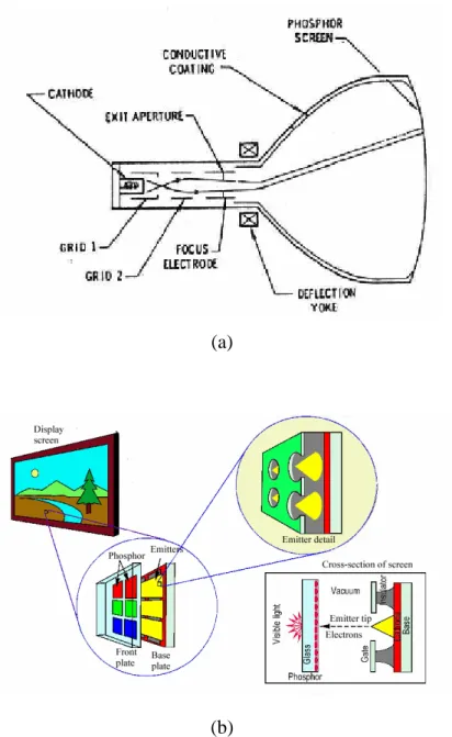
FED features all the pros of the CRTs in image quality and is flat and small volume. The schematic comparisons are revealed in Fig.1-2. The operation of CRTs involves
deflection of the beam in such a way that the electron spot scans the screen line-by-line. In FEDs, multiple electron beams are generated from the field emission cathode and no scanning of beams is required. The cathode is a part of the panel substrate consists of an X-Y electrically addressable matrix of field emission arrays (FEAs). Each FEA is located at the intersection of a row and a column conductor, with the row conductor serving as the gate electrode and the column conductor as the emitter base. The locations where the rows and columns intersect define a pixel. The pixel area and number of tips are determined by the desired resolution and luminance of the display. Typically, each pixel contains an FEA of 4-5000 tips. The emission current required for a pixel varies from 0.1 to 10 µA, depending on the factors such as the luminance of the display, phosphor efficiency and the anode voltage.
Compared to the active matrix LCDs, FEDs generate three times the brightness with wilder viewing angle at the same power level. Full color FEDs have been developed by various research groups from different aspects such as PixTech, Futaba, Fujitsu, Samsung, are presently engaged in commercially exploiting FED.
1.3 Recent Developments of Field Emission Devices for Field Emission Displays
FED is one of the most promising emissive type flat-panel display, which can overcome the drawbacks of TFT-LCD. However, some difficult technological subjects should be considered such as microfabrication of cathodes, assembly technology with accuracy of micrometer level, packaging of vacuum panel with thin-glass substrates, vacuum technology to keep stable field emission in small space of flat panels, selection
of suitable materials to keep a high vacuum condition in panels and high efficiency phosphor materials. The researching objects of this thesis is to produce novel cathode structure and synthesis of novel emitter materials for FED operations. The experimental background is introduced in the following sections.
1.3.1 Cathode Structures and Materials for Field Emission Displays
A.
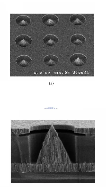
Spindt-type field emittersFigure 1-3 demonstrated the scanning electron microscope (SEM) image of a spindt type field emission triode [1.26], which was invented by Spindt of SRI and improved for the electron source of high-speed switching devices or microwave devices [1.27]. Meyer of LETI presented the capability of using Spindt-type emitters for a display in 1970s [1.28] and stabilized the field emission from Spindt-type emitters by introducing a resistive layer as the feedback resistance. This proposal triggered the development of field emitters as an electron source of displays by researchers and electronics makers in 1990. The merits of the Spindt type field emitters are summarized as following: (1) High emission current efficiency, more than 98% anode current to cathode current can be achieved for the symmetric structure of Spindt tip and the gate hole, the lateral electric field to the metal tip can be cancelled out. (2) The fabrication is self-aligned, easy process; uniform field emission arrays can be fabricated easily. Some research groups have successfully fabricated commercial FED products based on Spindt type field emitters such as Futaba, Sony/Candesent, Futaba and Pixtech.[1.29], the products above mentioned companies are shown in Figures 1-4.
However, there are some existing drawbacks of Spindt type field emitters when fabricating Spindt type FED such as (1) High gate driving voltage required; for a Spindt type field emission triode with 4 µm gate aperture, the driving voltage is typically more than 60 V, which results in the high cost of the driving circuits. To reduce the gate driving voltage, frontier lithography technologies such as E beam lithography must be applied to reduce the gate aperture to the sub-micron level. (2) The emission property degrades for the chemically instable of the metal tips. (3) Huge, expensive high vacuum deposition system required during fabricating large area Spindt type FED.
B. Si tip field emitters
An alternative approach to fabricate tip type field emitters is to fabricate the Si tip field emitters based on the semiconductor fabricating process. Figures 1-5(a) and (b) depict the SEM micrographs of Si tips array and Si tip field emission triodes array formed by chemical mechanical polishing (CMP) [1.30] Symmetric device structure and similar advantages with Spindt type field emitters can be obtained, However, high temperature oxidation sharpening process [5] prohibits Si tip from large area fabrication.
C. Carbon and Nano-sized Emitters
Carbon nanotubes have attracted a great deal of interests owing to their advantageous properties, such as high aspect ratios, small tip radius of curvature, high Young’s modulus, capability for the storage of a large amount of hydrogen, and structural diversities that make it possible for band gap engineering. These useful properties of carbon nanotubes (CNTs) make themselves good candidates for various applications, for
instance, wires for nanosized electronic devices, super strong cables, AFM tips, charge-storage devices in battery, and field emission display.
According to Fowler-Nodheim theory, the electric field at the apex of a needle-shaped tip is enhanced by a factor β = h/r, where h is the height of the tip and r is the radius of curvature of the tip apex. The carbon nanotube is a stable form of carbon and can be synthesized by several techniques. They are typically made as threads about 10-100 nm in diameter with a high aspect ratio (>1000). These geometric properties, coupled with their high mechanical strength and chemical stability, make carbon nanotubes attractive as electron field emitters. Several groups have recently reported good electron field emission from nanotubes [1.31-1.33].
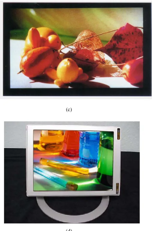
In 1999, Samsung pronounced a 4.5-inch carbon nanotube based field emission display. They mixed a conglomeration of single-walled CNTs into a paste with a nitrocellulose binder and squeezed the concoction through a 20-µm mesh onto a series of metal strips mounted on a glass plate. As the CNTs emerged from the mesh, they were forced into a vertical position. The metal strips with the CNTs sticking out of them served as the back of the display. The front of the display was a glass plate containing red, green, and blue phosphors and strips of a transparent indium-tin-oxide anode running from side to side. The glass plates were separated by spacers with the thickness of 200 µm. Once assembled, the edges were sealed and air was pumped out of the display. Samsung’s field emission display (Fig. 1-6) could be the precursor of a new generation of more energy efficient, high performance flat panel displays for portable computers [1.34]. The CNTs appear to be durable enough to provide the 10000hr lifetime
considered being a minimum for an electronic product. The panel consumes just half the power of an LCD to generate an equivalent level of screen brightness. They could also be cheaper than LCDs or other types of field emission displays being developed. Until now, at last five major Japanese electronic manufactures are working on this technology.
1.4 Motivation
Fabricating field emission cathodes with low operation voltage, high emission current, excellent stability and good reliability is crucial to commercialize the field emission display. According to the F-N equation, to achieve the high emission currents at low applied voltages, the work function φ of the cathode material must be as low as possible and the field-enhancement factor β and emission area α should be as large as possible.
To obtain a large β, the conventional method is to produce sharp tips, which reqired special techniques or complicated fabrication process, such as large oblique-angle thermal evaporation or sputtering to produce sharp metal cones, high temperature oxidation to sharpen silicon tips, or anisotropic etching of silicon using KOH to fabricate sharp tip molds.
In this thesis, sharp edge of the thin metal film as the field emitters was obtained by sputtering (increasing the field enhancement factor β), no special or complicated fabrication process was required. Fabricating the metal film into the chimney shape emitter also increased the field emission area α. An extraction gate structure was also proposed to fabricate the triode type chimney shape field emission array to reduce the
driving voltage.
Carbon nanotubes (CNTs) were also synthesized as the field emitters for the nanosized feature, which can provide large aspect ratio to increase the field enhancement factor β. The high density of the nanotubes also provides the large emission site density (increasing the emission area α). Different kinds of CNTs are synthesized using microwave plasma-enhanced chemical vapor deposition (MPCVD) and field emission properties of the CNTs are also investigated. The field emission characteristics of the CNTs with different morphology suggested that the field enhancement factor β is strongly affected by the density of CNTs. For high-density CNTs, the field-screening effect reduces the β value and the emission current. A good control of density and surface morphology of CNTs is thus required for future applications. To effectively control the densities of nanotubes, a post treatment process via excimer laser treatment was proposed. Furthermore, a novel process for controlled density growth of CNTs was also proposed in this thesis.
Additionally, a high anode voltage of more than 200 V is required to excite the phosphor resulted in the extremely high driving voltage of diode-type CNT emitters. To reduce the required driving voltage, two kinds of CNT triodes are proposed and characterized.
1.5 Thesis Organization
The overview of vacuum microelectronics and basic principles of field emission theory was described in chapter 1.
Improvement of the field emission characteristics of carbon nanotubes by high-density-plasma post treatment and pattern dimension were revealed in chapter 2.
The insulated gate structure field emission triode that avoid the short circuit problem between cathode and gate was demonstrated in chapter 3.
Finally, the conclusions and recommendations for future researches are provided in chapter 4.
Chapter 2
Improvement of the Field Emission Characteristics of Carbon
Nanotubes by High-Density-Plasma Post Treatment and Pattern
Dimension
The density of carbon nanotubes (CNTs) deposited by microwave plasma enhanced chemical vapor deposition (MPECVD) is extremely high, which results in the screening effect in the electric field. To achieve the excellent field emission characteristics, a post treatment by plasma was introduced to reduce the density of CNTs. The micrographs taken by scanning electron microscopy (SEM) showed the reduced density of CNTs, and the electrical characteristics revealed the improved field emission properties under suitable plasma treatment conditions. The turn-on field decreased from 0.9 V/µm to 0.19 V/µm, and the emission current density increased to 2.38 mA/cm2 at the applied field at
0.8 V/µm. Different pattern dimension arranged in a 1mm2 square were used to increase
the total emitting area. No extra process like plasma post treatment would be applied. And it successfully lower the turn on field from 0.9 V/µm to 0.48 V/µm.
2.1 Introduction
Carbon nanotubes (CNTs) grown on the cathode of an arc discharge were first observed by Iijima in 1991 [2.1], in which the needle-like tubes consist of coaxial tubes
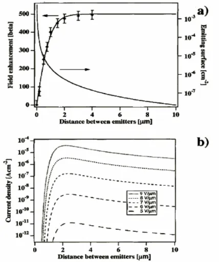
of graphite and range from 4 to 30 nm in diameter and 1 µm in length. The discovery of multi-walled carbon nanotubes (MWNTs) has attracted considerable interests because of their own unique physical properties and potential for the variety of applications [2.2-2.4]. Due to its geometrical properties, such as high aspect ratios, small tip radii of curvature, and high electrical conductivity, CNTs exhibit the excellent field emission characteristics. Nowadays, CNTs can be produced by arc discharge [2.5-2.6], laser ablation [2.7], thermal chemical vapor deposition [2.8-2.9], and microwave plasma-enhanced chemical vapor deposition [2.10]. However, the diameter distribution and the density of CNTs still cannot be controlled effectively. The screening effect of the dense arrangement CNTs by electric field has been reported. [2.11-2.13]. The density of CNTs at the film surface determines the emission sites density (ESD). If the CNTs are too closely packed, the electric field will be screened out. Groning et al. reported the field enhancement factor β of the tips decreases rapidly when the intertip spacing is smaller than twice the length of the tips. They also found that the maximum current density was obtained when the spacing between the tips is about two times of their relative heights by simulations, as shown in Fig. 2-1. For larger spacing, the current density decreases due to the decreasing density of the tips, with a nearly constant emission current per tip as the field enhancement factor remains constant. For smaller spacing the current density decreases rapidly due to the decreasing β factor and this effect cannot be compensated for by the quadratically increasing density of the emitting tips. This shows that when the spacing between the emitting structures on a surface becomes comparable to its length, problems of shielding do occur and will limit the emission current density.
optimized. However, the density of CNTs synthesized by MPECVD is too high and is difficult to control. In this chapter, a novel process using high density plasma was proposed to modify the density of CNTs grown by MPECVD. Different plasma generating power and etching time were utilized to obtain various arrangements of CNTs. The experimental results reveal the high emission current density and low turn-on field of CNTs can be achieved under suitable plasma treatment conditions.
2.2 Experimental Procedures
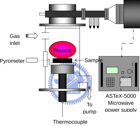
2.2.1 MPECVD Process
In this study, we have grown multi-walled carbon nanotubes (MWNTs) on Ni-coated Si surface by MPECVD (Fig. 2-2), which has been previously reported as a useful tool for the growth of MWNTs. The growth mechanism of carbon nanotubes by MPECVD involves three steps: (1) decomposition of hydrocarbon gas, (2) incorporation of carbon atoms into the transition metals, and (3) diffusion of carbon atoms in the catalyst metals to form the nucleation seeds for the nanotubes (Fig. 2-3). For the growth of CNTs by MPECVD using catalyst metals, both base-growth mode and tip-growth mode appear to be possible [2.14]. In the base-growth mode, the CNTs were formed by extrusion, resulting in a closed top end. In contrast, in the tip-growth mode, a metal catalyst particle remained on the top of each nanotube during growth. In our synthesis, the growth mode of CNTs seemed to be tip-growth mode, since the Ni droplets were observed to be on the tops of the CNTs (Fig. 2-4). In this mode, CH gas molecules were
dissolved into carbon by the H2 plasma, and then carbon atoms absorbed by the catalyst
and formed into nanotubes. During growth, the Ni domain was pushed upwards by the carbon nanotubes and formed a metal cap on the top of the nanotubes.
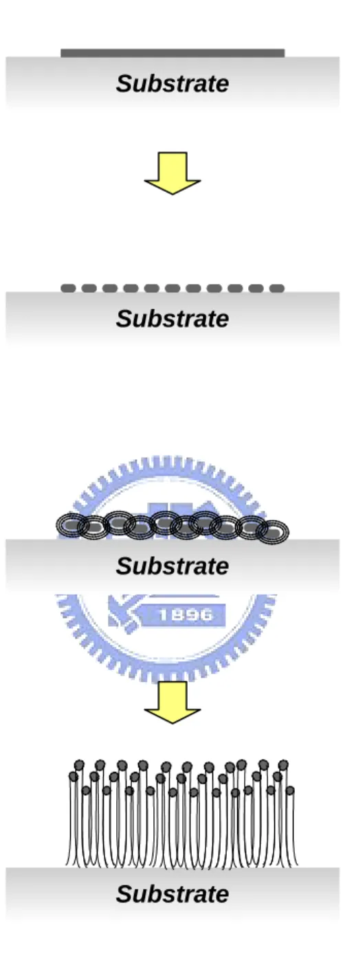
The experimental procedures of CNTs treated with plasma post treatments are shown schematically in Fig 2-5. As shown in Fig 2-5 (a), a 1μm-thick photoresist was spin-coated on a n-type Si(100) substrate and 1mm square cells were patterned by photolithography. Then a thin Ni layer (~3.5 nm) was deposited directly on the patterned Si substrate by electron beam evaporation system [Fig.2-5 (b)]. Then the Ni patterns were formed after the photoresist was removed by lift-off method as depicted in Fig. 2-5 (c). Finally, carbon nanotubes were grown selectively on the Ni patterns by microwave plasma enhanced chemical vapor deposition (MPECVD) system that was shown in Fig. 2-5 (d). CH4 and H2 were used as the source gases and typical flow rates were 10 and 100
sccm, respectively. The microwave power was kept at 1.2 kW and the chamber pressure was held at 30 torr. The hydrogen plasma was introduced first to change the Ni layer into Ni nano particles. Then CH4 was dissolved in the hydrogen plasma and transition metals
would adsorb carbon atoms to form nanotubes. The substrate temperature during growth was estimated at about 500℃ and typical growth time was 5 minutes.
2.2.2 Inductively Coupled Plasma (ICP) Process
Plasma processes are widely used in semiconductor technology. For example, free radicals significantly enhance sputtering deposition, etching, and CVD films stress control processes. For etching process, lower pressure results in longer mean free path,
and less collisional scattering, which improve etching profile control. In a conventional capacitively coupled plasma source cannot generate high density plasma , the ion flux and ion energy of the plasma source are dependently on RF power. It is crucial for a plasma source to be able to control both ion flux and ion energy. Inductively coupled plasma can generate high density plasma at few mTorr with the ability of controlling both ion flux and ion energy.
CNTs were treated by the plasma post treatment in a inductively coupled plasma system [Fig.2-5 (e)].The pressure of ICP system was 10mTorr. The flow rate of argon and oxygen were 20 and 20 sccm, respectively.The density of carbon nanotubes were modified by ICP RF power and etching time. The parameters of ICP power and etching time are listed in table 2-1.
2.2.3 Measurement System for Vacuum Microelectronic Devices
A high-vacuum measurement environment was set up to characterize the field emission properties of carbon nanotubes (Fig. 2-6). The vacuum chamber is evacuated by a turbo pump. Cathode contact is made directly on the wafer. The anode plate is a glass plate coated with an ITO layer and a P22 phosphor. All cables were shielded except for the ground return path to the power source. The DC measurement system is based on the Keithley 237 high-voltage source units with IEEE 488 interface. The measurement instruments are auto-controlled by the computer. During the measurement, the spacing between the emitter (cathode) and controller (anode) was controlled to be constant at 500 um and the base pressure in the testing chamber was about 1.0×10⁻⁶ Torr. Field emission
characterization was obtained from the CNTs films over a voltage sweep from 0 V to 1000 V and the area of the films is 1mm2.
2.3 Results and Discussion
2.3.1 The Effect of Plasma Post Treatment
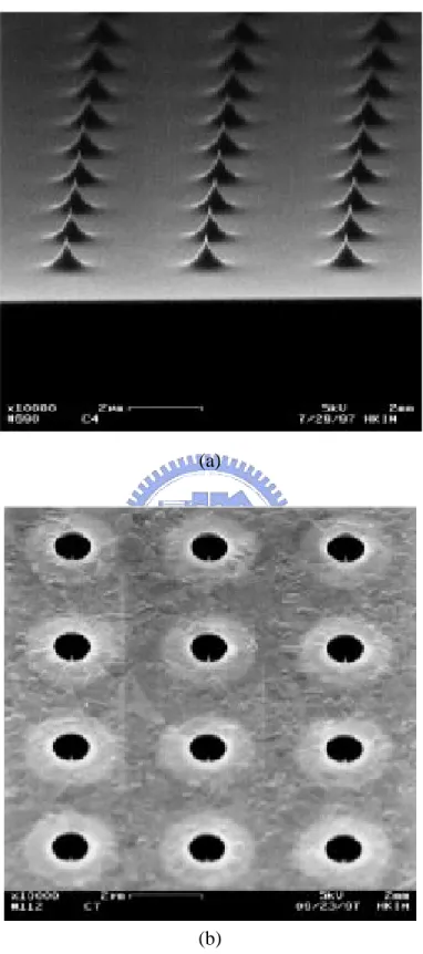
Fig. 2-7 shows a Scanning Electron Microscopy (SEM) micrograph of patterned CNT array grown by MPECVD. It can be seen that CNTs were grown only on the pattern of catalytic metal but not on the plain Si substrate. The vertically aligned and high density of nanotubes was discovered in Fig. 2-8. The average height of the CNTs is about 20 µm, as shown in Fig. 2-7(b), and the diameter of CNTs ranges from about 30 nm to 60 nm, as shown in Fig. 2-8(b). The reason of the aligned nanotubes growth attributed to the high density of CNTs grown from the densely packed catalytic nanoparticles. As the nanotubes lengthen, the interaction between nanotubes by Van der Waals force to form a large bundle with some rigidity, which enables them to continue growing along the same direction.
Fig. 2-9 shows the SEM micrographs of CNTs treated under O2 + Ar plasma
treatment condition of gas flow rate 20 and 20 sccm, respectively. The etching time is 60 seconds. Different inductive-coupled-plasma generation power: (a) untreated, (b) 200W, (c) 300W and (d) 400W were used. The density of the CNTs decreases as plasma generation power increases, which results from the destruction of CNTs during plasma
treatment. The corresponding cross-sectional views of CNTs are illustrated in Fig. 2-10. For the RF generation power of 200W, parts of the CNTs were destroyed by plasma and the length variation of CNTs increased. For the generation power of 400W, more CNTs were significant broken and turn-on field increased. (Fig. 2-11).
Fig. 2-12 indicates the SEM micrographs of CNTs treated by generated-plasma power of 300W with different etching time. Consistent destruction of CNTs was achieved with a longer plasma etching time, corresponding cross-sectional views of CNTs are shown in Fig. 2-13. For the case of 30 seconds [Fig. 2-13(a)], the length of CNTs and the density of CNTs were not changed obviously. For the case of 90 seconds [Fig.2-13(c)], most of the CNTs were destroyed by the plasma. The average length of CNTs was decreased to only 1 µm. Similar results were found in the case of generated-plasma power of 200W and 400W with different etching time [Fig.2-15 and Fig.2-16]. We found the CNTs almost destroyed at the condition of RF power 400W and etching time 90s [Fig.2-16(c)]. Its field emission characteristics become worse due to high energy and long time bombardment of CNTs.
The emission characteristics of the CNTs for different plasma treatment conditions are shown in Fig. 2-11, Fig. 2-14, and Fig. 2-17. Nine samples including non-PPT CNTs, PPT-CNTs A (200W and 30s ),PPT-CNTs B (200W and 60s), PPT-CNTs C (200W and 90s), PPT-CNTs D (300W and 30s), PPT-CNTs E (300W and 60s) , PPT-CNTs F (300W and 90s) , PPT-CNTs G (400W and 30s) , PPT-CNTs H (400W and 60s) , PPT-CNTs I (400W and 90s) are compared. With an applied electric field of 0.8 V/µm, the emission current densities were 15 mA/cm2 for the CNTs treated under the PPT condition of 200W and 60s. The corresponding Fowler-Nordheim plots for CNTs with different PPT
conditions were plotted in Fig. 2-11(b), Fig. 2-14(b), and Fig. 2-17(b). The linearity slope of the plots confirms the field emission phenomena.
The turn-on electrical field of the CNTs field emission diode, which was defined as the field at which the current density is 10µA/cm2 , decreases from 0.9 V/µm to 0.19
V/µm for the untreated CNTs and the PPT-CNTs with generated power of 300 Wand
etching time of 60s . Table2-2 shows the relationship between different PPT conditions and the field emission properties.
2.3.2 The Effect of Pattern Dimension
Fig.2-18 shows the electric field distribution on densely packed CNTs. As the figure demonstrated, we found only the CNTs in the edge easily emitted electron because of the strong electric field. Different pattern dimension arranged in a 1mm2 square were used to increase the total emitting area. Fig.2-19 shows the 1000µm, 100µm and 10µm pattern size and its number in a square were 1, 25, 2500, respectively. The field emission characteristics were showed in Fig.2-20. The turn on field decreased from 0.9 V/µm to 0.48 V/µm. The center of packed CNTs were affected by weaker electric field distribution and the electron would be screened out. The large, medium and small patterns have 4000µm, 10000µm, 100000µm edge length, respectively. The increase of total edge length improve the field emission characteristics. It is the reason that nearly CNTs in the edge would be thought the efficient emitting area. In this method, we can lower the turn-on voltage without extra process like plasma post treatment. By proper configuration designs, the turn-on voltage and current density would be improved.
2.4 Conclusions
The modification of surface morphology of CNTs has been achieved by O2 + Ar
plasma post treatments. The SEM micrographs revealed the surface distribution of CNTs after plasma post treatments. For the generated plasma power of 200W and 300W, parts of CNTs were shortened and the remaining CNTs protruded from the surface of CNTs films. When the generated plasma power increased to 400W, most of the CNTs were shortened and less protruding CNTs were observed. The field emission characteristics confirmed the improvement of field emission properties under suitable PPT conditions, the field emission current density increased to 2.38 mA/cm2 at the electric field of 0.8
V/µm and the turn-on electric field decreased from 0.9 V/µm untreated to 0.19V/µm for PPT conditions of generated power of 300Wand etching time of 60s . The experimental results reveal that improved emission properties can be achieved by optimizing the density and the length variation of CNTs under proper plasma treatment conditions.
The center of packed CNTs were affected by weaker electric field distribution and the electron would be screened out. The increase of total edge length improve the field emission characteristics. It is the reason that nearly CNTs in the edge would be thought the efficient emitting area. In this method, we can lower the turn-on voltage without extra process like plasma post treatment. By proper configuration designs, the turn-on voltage and current density would be improved.
Chapter 3
Fabrication and Characterization of Insulated Gate Structure Field
Emission Device Based on Carbon Nanotubes
In this chapter, a insulated gate structure field emission device based on carbon nanotubes (CNTs) is proposed and the experimental results are reported. The distance between polysilicon gate and the CNTs cathode was determined by the wet etching process. Thus, the interelectrode gap is easily formed in good uniformity and reproducibility with dimensions below 1 micrometer. The CNTs were selectively grown
by microwave plasma enhanced chemical vapor deposition system (MPECVD). The effect of gate-to-emitter gap and length of carbon nanotubes were controlled to
investigate the relation between the field emission current and applied voltage .The turn–on voltage of the fabricated device with interelectrode gap of 1 um is 18 volt, and the emission current density is as high as 0.1 mA/cm2 at gate voltage 136 volt. The emission current fluctuation is about ± 5.5% for 1500sec.
3.1 Introduction
CNTs have attracted increasing attention owing to the promising applications in vacuum microelectronics. Several groups [3.1-3.5] have demonstrated the low turn on electric field properties and extremely large emission current of the CNTs field emission diodes. However, the driving voltage of the diode type field emission devices is still too
high. To lower the driving voltage is crucial for the applications of field emission devices such as field emission displays to cost down the driving circuits. Triode types of field emission devices employing arc-produced CNTs were therefore demonstrated to reduce the driving voltage. Lee, et al [3.6] have fabricated a gated CNT-FED by employing a metal mesh as the gate electrode and achieved the turn-on voltage of 100 V. Wang, el
al [3.7] have demonstrated a triode type field emission display with a specific filling
method to reduce the operation voltage; the low turn-on voltage of about 25 volt was achieved and the emission current reaches 0.3 µA as the gate voltage was 50 volt. To increase the gate induced electric field by decreasing the gate aperture is essential to lower the gate voltage. However, reduction of the gate aperture is difficult using conventional arc-produced CNTs. In this work, CNTs field emission triodes were fabricated by IC fabrication process and selective growth of CNTs via MPCVD. The fabricated device accomplished the low turn-on voltage of 18 volt and the extremely high emission current of 5 µA as the gate voltage reaches 136 volt.
3.2 Experiment Procedures
The fabrication procedure of the carbon nanotubes insulated gate structure field emission device is shown schematically in Fig. 3-1. As shown in Fig. 3(a), initially, the 500-nm-thick thermal oxide was grown on a N-type Si(100) substrate at 1050℃. The 200-nm-thick poly-Si was then deposited on the thermal oxide by low pressure chemical vapor deposition(LPCVD) using pure SiH4 at 590℃. The poly Si was further doped with
phosphorous using solid diffusion source(PH-1000N) at 950℃ for 30 minutes and then phosphorous was driven in at 950℃ for 30 minutes. Finally, a 200-nm-thick nitride layer was deposited on poly-Si. The sheet resistance of poly-Si was 50 Ω/□ by 4-point probe. A
1-μm-thick photoresist was spin coated, and patterned by photolithography. First, The nitride, poly-Si and SiO2 layers were dry etched by the ICP-RIE using Cl2, SF6, and O2
mixture or CHF3, Ar mixture. Then, the poly-Si layer was continuously etched by the wet
etching solution of poly etcher. Employing the previously patterned photoresist layer as the shadow mask, a thin nickel layer (3.5nm) was deposited directly on the patterned Si substrate as the catalyst metal by electron beam evaporation system, and the catalyst layer was thus formed after the photoresist was removed by the lift-off method as depicted inFig.3-1(d) and Fig. 3-1(e). Finally, carbon nanotubes were grown selectively on the nickel layers by microwave plasma enhanced chemical vapor deposition. CH4, N2
and H2 were used as the source gases and the flow rates were 20, 80 and 80 sccm,
respectively. The microwave power was kept at 1.2kW and the chamber pressure was set at 35 Torr. The substrate temperature was estimated at about 500℃ and the deposition time was 2 minutes.
The growth morphology of CNTs was observed by scanning electron microscopy (SEM) and the field emission properties of CNTs triodes were characterized in a high-vacuum environment with a base pressure of 1.0×10⁻⁶ Torr. A schematic diagram of
the experimental setup is shown in Fig. 2-6. A glass plate coated with indium-tin-oxide (ITO) and phosphor was used as an anode and positioned 500 µm above the carbon nanotubes. The anode current was measured as a function of the gate voltage and anode voltage using Keithley 237 high voltage units with an IEEE 488 interface controlled by a personal computer.
3.3 Results and Discussion
3.3.1 Comparison Electrical Characteristics between Conventional and
Insulated Gate Structure Triode
The SEM micrograph of the conventional CNTs field emission triode is shown in Fig. 3-2. The CNTs were selectively grown on the catalyst metal within the cathode region. It can be seen that CNTs are easily grown over the gate height. Carbon nanotubes bended because of its superior length. CNTs touched the gate and cause the short circuit problem when gate is applied voltage due to the metallic conductivity.Fig. 3-2(b) shows short circuit electrical characteristics. Fig.3-3(a) shows the gate voltage versus the anode voltage. The gate can build a electric field to induce the electron emitting and can be a switch or modulate the gray-scale. In a conventional structure, gate
leakage current would increase as the gate voltage increase [Fig.3-3(b)]. Thus, the emitting electrons to anode plate would decrease at the same time. To solve the problem before, a insulated gate structure triode was demonstrated in Fig.3-4. We control the carbon nanotubes length about 1µm and use the wet etching process to etch the poly gate. Fig.3-4(a) shows the top view of insulated gate structure and Fig.3-4(b) is the cross section of it. From the figure, the insulated layer avoids the touch between gate and emitters. It successfully solves the short circuit problem by depositing an insulated layer. Fig. 3-5 indicates emission current-voltage characteristics of insulated gate structure CNTs triode. The emission currents (Ia) were measured as a function of gate voltage (Vg)
sweep from 0 to 150. The voltage-current plot shows a good rectifying property. The turn-on voltage (Von) defined at which the anode current was 10µA/cm2. Low turn-on
voltage was achieved at 18 V for the insulated gate structure triode with 1.2µm interelectrode. Fig.3-6 reveals the field emission current versus anode voltage under different gate bias. With the increase of gate voltage, the anode turn on voltage would decrease because the larger gate bias can build a greater electric field to induce the electrons. The gate operation voltage might be reduced by decreasing the gate-to-emitter gap and the CNTs length.
3.3.2 Gate Leakage in Conventional and Insulated Gate Structure
Triode
increase. It would cause the anode current decreasing [Fig.3-3]. A measurement of gate voltage and current was established at anode voltage 450 V and gate voltage swept from 0 to 100 V. The result was revealed in Fig.3-7. The gate leakage current almost remains constant and is not a function of gate voltage. Comparison with the conventional structure, it not only avoid the short circuit problem between gate and emitters but also reduce the gate leakage current to improve the anode current performance.
3.3.3 Field Emission Current Stability
A emission current stability test was performed on the insulated gate structure CNT triode. An average emission current (I0) of 2.64 µA was established at the anode voltage
of 450 V, gate voltage of 30 V and cathode voltage grounded. The emission current reliability over a short term period of 1500 seconds is shown in Fig.3-8. No obvious degradation of emission current was observed and the fluctuation was about ±5.5%.
3.4 Summary and conclusions
Based on the selective growth of CNTs via the MPECVD, the insulated gate structure was fabricated. The distance between polysilicon gate and the CNTs emitter was determined by the wet etching process. Thus, the interelectrode gap is easily formed in good uniformity and reproducibility with dimensions below 1 µm. The turn–on voltage of the fabricated device with interelectrode gap of 1.2 µm is 18 volt, and the emission current density is 0.1 mA/cm2 at gate voltage 136 volt. The emission current fluctuation
Chapter 4
Conclusions and Future Prospects
Conclusions
The modification of surface morphology of CNTs has been achieved by O2 + Ar
plasma post treatments. The SEM micrographs revealed the surface distribution of CNTs after plasma post treatments. For the generated plasma power of 200W and 300W, parts of CNTs were shortened and the remaining CNTs protruded from the surface of CNTs films. When the generated plasma power increased to 400W, most of the CNTs were shortened and less protruding CNTs were observed. The field emission characteristics confirmed the improvement of field emission properties under suitable PPT conditions, the field emission current density increased to 2.38 mA/cm2 at the electric field of 0.8 V/µm and the turn-on electric field decreased from 0.9 V/µm untreated to 0.19V/µm for PPT conditions of generated power of 300Wand etching time of 60s . The experimental results reveal that improved emission properties can be achieved by optimizing the density and the length variation of CNTs under proper plasma treatment conditions.
The center of packed CNTs were affected by weaker electric field distribution and the electron would be screened out. The increase of total edge length improve the field emission characteristics. It is the reason that nearly CNTs in the edge would be thought the efficient emitting area. In this method, we can lower the turn-on voltage without extra process like plasma post treatment. By proper configuration designs, the turn-on voltage and current density would be improved.
Based on the selective growth of CNTs via the MPECVD, the insulated gate structure was fabricated. The distance between polysilicon gate and the CNTs emitter was determined by the wet etching process. Thus, the interelectrode gap is easily formed in good uniformity and reproducibility with dimensions below 1 µm. The turn–on voltage of the fabricated device with interelectrode gap of 1.2 µm is 18 volt, and the emission current density is 0.1 mA/cm2 at gate voltage 136 volt. The emission current fluctuation is about ± 5.5% for 1500 seconds.
Future Prospects
For the synthesize of carbon nanotubes for field emission devices, the further research topics are proposed as follows:
(1) Low temperature (below 450 oC) growth of CNTs.
(2) Pretreatment of the catalyst for reduced density growth of CNTs.
(3) Post treatment of CNTs such as rapid thermal treatment, plasma treatment or ion bombardment to reduce the density of CNTs.
(4) Surface coating with ultra-thin metals to enhance the field emission property of CNTs.
For the field emission property investigation of CNTs (1) The long-term reliability should be investigated.
conditions) should be discussed.
For the CNT triodes, the further research topics are proposed as follows: (1) The gate-to-emitter gap can be further reduced to lower the turn-on voltage.
(2) Optimal gate structure or insulated gate surface for the CNT triodes should be developed to reduce the gate current.
(3) The focus gate can be applied to the CNT triodes to improve the emission characteristics.
(4) To demonstrate a prototype of CNT FED.
Finally, for the applications of CNTs in vacuum microelectronics, the further research topics are proposed as follows:
(1) Fabrication of CNTs lateral field emission device for high frequency and high power circuit applications.
References
Chapter 1
[1.1] S. M. Sze, “Physics of semiconductor devices”, 2nd ed., John-Wiley & Sons
pulisher, New York, p. 648, 1991.
[1.2] R. H. Fowler and L. W. Nordheim, “Electron emission in intense field,” Proc.
R. SOC. A229, p. 173, 1928.
[1.3] C. A. Spindt, I. Brodie, L. Humpnrey, and E. R. Westerberg, “Electrical
properties of thin-film field emission cathodes with molybdenum cones,” J.
Appl. Phys., Vol. 47, p. 5248, 1976.
[1.4] R. Meyer, “Recent development on microtips display at LETI,” IVMC’91
Technical Digest, p. 6, 1991.
[1.5] N. E. McGruer and K. Warner, “Oxidation-sharpened gated field emitter
array process,” IEEE Trans. Electron Devices, Vol. 38, No. 10, p. 488, 1991.
[1.6] S. E. Huq and L. Chen, “Fabrication of sub-10 nm silicon tips: a new
approach,” J. Vac. Sci. & Technol. B, Vol. 13(6), p. 2718, 1995.
[1.7] D. W. Branston and D. Stephani, “Field emission from metal-coated Silicon
tips,” IEEE Trans. Electron Devices, Vol. 38, No. 10, p. 2329, 1991.
[1.8] V. V. Zhirnov and E. I. Givargizov, “Field emission from silicon spikes with
[1.9] J. H. Jung and B. K. Ju, “Enhancement of electron emission efficiency and
stability of molybdenum field emitter array by diamond-like carbon
coating,” IEEE IEDM’96, p. 293, 1996.
[1.10] R. E. Burgess, H. Kroemer, and J. M. Honston, “Corrected value of
Fowler-Norheim field emission function v(y) and s(y),” Phys. Rev., Vol. 1,
No. 4, p. 515, May, 1953.
[1.11] R. B. Marcus, T. S. Ravi, T. Gmitter, H. H. Busta, J. T. Niccum, K. K. Chin,
and D. Liu, “Atomically sharp silicon and metal field emitters,” IEEE Trans.
Electron Devices, Vol. 38, p. 2289, 1991.
[1.12] P. Vaudaine and R. Meyer, “Microtips fluorescent display,” IEEE IEDM’91, p.
197, 1991.
[1.13] C. Curtin, “The field emission display,” International Display Research
Conference p. 12, 1991.
[1.14] C. A. Spindt, C. E. Holland, I. Brodie, J. B. Mooney, and E. R. Westerberg,
“Field-emitter array applied to vacuum fluorescent displays,” IEEE Trans.
Electron Devices, Vol. 36, No. 1, p. 225, 1989.
[1.15] David A. Cathey, “Field emission displays,” Information Display, p. 16, Oct.,
1995.
Electronics ASIA, p. 42, Nov., 1995.
[1.17] H. G. Kosmahl, “A wide-bandwidth high-gain small size distributed amplifier
with field-emission triodes (FETRODE’s) for the 10 to 300 GHz frequency
range,” IEEE Trans. Electron Devices, Vol. 36, No.11, p. 2715, 1989.
[1.18] P. M. Larry, E. A. Netteshiem, Y. Goren, C. A. Spindt, and A. Rosengreen,
“10 GHz turned amplifier based on the SRI thin film field emission
cathode,” IEEE IEDM’88, p. 522, 1988.
[1.19] C. A. Spindt, C. E. Hollard, A. Rosengreen, and I. Brodie, “Field emitter
array development for high frequency operation,” J. Vac. Sci. & Technol. B,
Vol. 11, p. 486, Mar./Apr., 1993.
[1.20] C. A. Spindt, “Microfabricated field emission and field ionization sources,”
Surface Science, Vol. 266, p. 145, 1992.
[1.21] T. H. P. Chang, D. P. Kern, et al., ”A scanning tunneling microscope
controlled field emission micro probe system,” J. Vac. Sci. & Technol. B,
Vol. 9, p. 438, Mar./Apr., 1991.
[1.22] H. H. Busta, J. E. Pogemiller, and B. J. Zimmerman, “The field emission
triode as a displacement/process sensor,” J. Micromech. Microeng., p. 45,
1993.
IEEE Transducers- International Solid-State Sensors and Actuators, p. 126,
1991.
[1.24] D. G. Fink and D. Christiansen, Electronic Engineering Handbook,
Mcgraw-Hill, New York, 1989.
[1.25] H. Imura, S. Tsuida, M. Takahasi, A. Okamoto, H. Makishima, and S.
Miyano, “Electron gun design for traveling wave tubes (TWTs) using a field
emitter array (FEA) cathode,” IEEE IEDM’97, p. 721, 1997.
[1.26] S. Itoh, T. Watanabe, T. Yamaura, and K. Yano, “A challenge to field
emission displays,” in Proc. Asia Display, Oct. 1995, pp. 617–620.
[1.27] C. A. Spindt, I. Brodie, L. Humphrey, and E. R. Westerberg,“Physical
properties of thin-film field emission cathodes with molybdenum cones,” J.
Appl. Phys., vol. 47, no. 12, pp. 5248–5263, 1976.
[1.28] R. Meyer, A. Ghis, P. Rambaud, and F. Muller, “Microtips fluores-cent
display,” in Proc. Japan Display, Sept./Oct. 1986, pp. 512–515.
[1.29] S. Itoh AND M. Tanaka, “Current Status of Field-Emission Displays”,
PROCEEDINGS OF THE IEEE, VOL. 90, NO. 4, APRIL 2002
[1.30] M. Ding, H. Kim, and A. I. Akinwande” Highly Uniform and Low Turn-On
Voltage Si Field Emitter Arrays Fabricated Using Chemical Mechanical
FEBRUARY 2000
[1.31] X. Xu and G. R. Brandes, “A method for fabricating large-area, patterned,
carbon nanotube field emitters,” Appl. Phys. Lett., Vol. 74, p. 2549, 1999.
[1.32] A. M. Rao, D. Jacques, and R. C. Haddon, “In situ-grown carbon nanotube
arrays with excellent field emission characteristics,” Appl. Phys. Lett., Vol.
76, p. 3813, 2000.
[1.33] H. Murakami, M. Hirakawa, C. Tanaka, and H. Yamakawa, “Field emission
from well-aligned, patterned, carbon nanotube emitters,” Appl. Phys. Lett.,
Vol. 76, p. 1176, 2000.
[1.34] W. B. Choi, D. S. Chung, J. H. Kang, H. Y. Kim, Y. W. Jin, I. T. Han, Y. H.
Lee, J. E. Jung, N. S. Lee, G. S. Park, and J. M. Kim, “Fully sealed,
high-brightness carbon-nanotube field-emission display,” Appl. Phys. Lett.,
.
Chapter 2
[2.1] S. Iijima, “Helical microtubules of graphitic carbon,” Nature, Vol. 354, p. 56,
1991.
[2.2] S. Saito, “Carbon nanotubes for next-generation electronics devices,” Science,
Vol. 278, p. 77, 1997.
[2.3] S. J. Tans and C. Dekker, “Molecular transistors: potential modulations along
carbon nanotubes,” Nature, Vol. 404, p. 834, 2000.
[2.4] Z. H. Yuan, H. Huang, H. Y. Dang, J. E. Cao, B. H. Hu, and S. S. Fan, “Field
emission property of highly ordered monodispersed carbon nanotube arrays,”
Appl. Phys. Lett., Vol. 78, p. 3127, 2001.
[2.5] J. M. Lauerhaas, J. Y. Dai, A. A. Setlur, and R. P. H. Chang, “The effect of
arc parameters on the growth of carbon nanotubes,” J. Mater. Res., Vol. 12, p.
1536, 1997.
[2.6] P. M. Ajayan, Ph. Redlich, and M. Ruhle, “Balance of graphite deposition and
multi-shell carbon nanotube growth in the carbon arc-discharge,” J. Mater.
Res., Vol. 12, p. 244, 1997.
[2.7] A.G. Rinzler , J. Liu , H. Dai , P. Nikolaev , C. B. Huffman , F. J.
Rodriguez-Macias , P. J. Boul , A. H. Lu , D. T. Colbert , R. S. Lee , J. E.
purification of single-wall carbon nanotubes: process, product, and
characterization,” Appl. Phys. A, Vol. 67, p. 29, 1998.
[2.8] J. M. Mao, L. F. Sun, L. X. Qian, Z. W. Pan, B. H. Chang, W. Y. Zhou, G.
Wang, and S. S. Xie, “Growth of carbon nanotubes on cobalt disilicide
precipitates by chemical vapor deposition,” Appl. Phys. Lett., Vol. 72, p.
3297, 1998.
[2.9] C. J. Lee, K. H. Son, J. Park, J. E. Yoo, Y. Huh, and J. Y. Lee, “Low
temperature growth of vertically aligned carbon nanotubes by thermal
chemical deposition,” Chem. Phys. Lett., Vol. 338, p. 113, 2001.
[2.10] Y. C. Choi, D. J. Bae, Y. H. Lee, B. S. Lee, G. S. Park, W. B. Choi, N. S. Lee,
and J. M. Kim, “Growth of carbon nanotubes by microwave
plasma-enhanced chemical vapor deposition at low temperature,” J. Vac. Sci.
& Technol. A, Vol. 18, No. 4, p. 1864, 2000.
[2.11] W. Lei, B. P. Wang, H. C. Yin, Y. X. Wu, and C. Z. Chang, “Influence of the
fringe field and the field interaction on the emission performance of a diode
emitter array,” Nuclear Ins. and Methods in Phys. Reaerch A, Vol. 451, p.
389, 2000.
[2.12] N. V. Egorov, and A. A. Almazov, “Optimization of multi-tip field emission
[2.13] O. Groning, O. M. Kuttel, C. Emmenegger, P. Groning, and L. Schlapbach,
“Field emission properties of carbon nanotubes,” J. Vac. Sci. & Technol. B,
Vol. 18, No. 2, p. 665, 2000.
[2.14] Y. Gao, J. Liu, M. shi, S. H. Elder, and J. W. Virden, “Dense Arrays of
Well-Aligned Carbon Nanotubes Completely Filled With Single Crystalline
Ttitanium Carbide Wires on Titanium Substrates”,Appl. Phys. Lett. 74, p.