國
立
交
通
大
學
材料科學與工程學系
碩 士 論 文
利用掃描穿隧顯微鏡觀察昆拉赫振盪及其應用
Application of Gundlach Oscillation by Scanning Tunneling
Microscopy
研究生:吳璧雰
指導教授:姚永德 教授
陳三元 教授
蘇維彬 教授
中 華 民 國 九 十 六 年 七 月
中文摘要--- i Abstract--- ii Acknowledge --- iii Figures--- v CHAPTER 1: Introduction --- 1 CHAPTER 2: Theory--- 4 2.1 Surface Science --- 4
2.2 Structure of Clean Surface- --- 5
2.2.1 Surface Relaxation--- 5 2.2.2 Surface Reconstruction --- 6 a. Au(111)--- --- 7 b. Ag/Cu(111)--- 9 2.3 Film Growth--- 10 2.3.1 Adsorption --- 11
2.3.2 Thin Film Deposition --- 12
a. Nucleation--- 12
b. Grain Growth --- 13
c. Coalescence --- 13
d. Film Growth --- 13
2.4.2 Density of State --- 18
2.5 Scanning Tunneling Spectroscopy --- 20
2.5.1 At Low Bias: Surface State (Bias<Φ)--- 21
2.5.2 At High Bias: Gundlach Oscillation (Bias>Φ)--- 22
CHAPTER 3: Experimental Setup --- 25
3.1 Experiment Instrument --- 25
3.2 Ultrahigh Vacuum System--- 26
3.2.1 Mechanical Rotary Pump--- 26
3.2.2 Turbo Molecular Pump --- 26
3.2.3 Baking--- 27
3.2.4 Ion Pump--- 27
3.2.5 Titanium Sublimation Pump (TSP) --- 27
3.2.6 Ionization Gauge--- 28
3.3 Sample Preparation--- 28
3.3.1 Ion sputtering--- 28
3.3.2 Annealing --- 29
3.3.3 Electron Beam Gun --- 30
3.4 Scanning Tunneling Microscopy (STM) --- 31
3.4.1 Tip --- 31
3.4.2 Scanning Mechanism--- 33
3.4.3 Scanner--- 34
3.4.4Vibration isolation--- 34
4.1 Energy Separation Measurement --- 36
4.1.1 Energy Separation in Uniform Ultrathin Film System --- 36
4.1.2 Energy Separation in Various Ultrathin Film System--- 40
4.1.3 Energy Separation in Single Atomic Ultrathin Film System --- 43
4.2 Dependence of Energy Separation on Tip--- 46
4.2.1 Interplay between Discontinuous Contrast and Energy Separation--- 46
4.2.2 Tip-Sample Field Influence in Energy Separation --- 47
4.3 Surface Profiling wit Variable Gundlach Oscillation --- 51
4.3.1 Dependence of Gundlach Oscillation on Distinct Surface Structures-51 4.3.2 Surface Mapping with Increasing Gap Width --- 53
4.3.3 Interplay between Gap Width and STM Image Resolution --- 58
CHAPTER 5: Conclusion--- 59
學生: 吳璧雰 指導教授: 蘇維彬 博士 姚永德 博士 陳三元 博士 國立交通大學材料科學與工程學系碩士班
摘 要
在本實驗中,我們以掃描穿隧顯微鏡(STM)和掃描穿隧能譜術(STS)觀察金屬 表面形貌以及昆拉赫振盪,昆拉赫振盪所觀察到的駐波態分佈會隨著表面材料及 結構的改變而有所差異。在 Cu(111)及重構的 Au(111)表面上鍍上 Ag 薄膜,透過 STS 的量測,發現基板與薄膜的高能量駐波態會有ㄧ定量差值。此現象不僅在均 勻薄膜中可見,在結構稍有差異的薄膜(Co/Cu(111)系統)及單原子薄膜系統中皆 有相似現象。根據本文所提出的模型,此定量差值是基板與薄膜的功函數差值, 且此功函數的差值與試片表面電場應無相依性。 在同ㄧ材質的表面(Ag/Cu(111)系統)上,也在不同結構上得到相異的駐波強 度。此差異可視為是因結構不同而造成的電子穿透率變動,當穿透率較小時,反 射造成的駐波強度會較為強烈。然而這些駐波強度會在能譜中呈現一種守衡的現 象,可見同一物質的相異結構會在駐波態有不同程度的反應。在 Z-V 能譜量測過 程中,當電壓逐漸上升,探針退後量亦會隨之增加。我們試著在探針遠離表面的 過程中,對重構的 Au(111)表面做影像分析,可得在探針距表面到 60Å 之遠時, 擁有較 1nm 為佳的解析能力。如此的技術非常適用於奈米碳管或 DNA 的觀察及電 性分析,遠距離的掃描可避免此類軟物質在掃描過程中被探針帶走,而高解析度 亦能確保電性量測的精確性。Tunneling Microscopy
Student: B. F. Wu Advisors: Dr. Y. D. Yao Dr. W. B. Su Dr. S. Y. Chen
Abstract
Scanning tunneling microscopy (STM) and scanning tunneling spectroscopy (STS) are employed in this thesis to study the surface topography and the Gundlach Oscillation on metal surface. The separations of standing wave states between the films and substrates vary with the characteristics of the surface. Constant energy separations between the film and substrates exhibit in uniform and various thin film systems. We proposed a model to explain the energy separation, and it is considered as the work function difference between the film and substrates. According to our result, the energy separations at higher bias are field-independent.
Our results also show that the intensity of Gundlach Oscillation varies with distinct structures. Higher intensity of Gundlach Oscillation occurs accompanied with lower transmissivity. However for the same material, the Gundlach oscillation intensities of distinct regions are conserved during Z-V measurement. It shows that different structures response distinctly at the energy of standing wave states. Observing reconstructed Au(111) surface with Z-V measurement, the resolution is better than 1.1nm even when the tip-sample displacement is large as 60Å. This technique is quite applicable in observing soft materials as carbon nanotubes or DNA. Generally soft materials tend to be dragged by the tip since the distance between the tip and sample is less than 10Å. Such dragging can be avoided if the scanning is
兩年前,因為老天爺的安排,讓我進了交通大學的材料所,也讓我得以擁有 這兩年中難能可貴的各種經驗。 首先感謝姚老師讓我有機會進入中研院做實驗,接觸國內學術界的最高點; 也謝謝蘇老師的指導及收留,讓我有機會接觸如此純物裡的學問,雖然只有半年 的實驗時間,但多虧有老師的指導,仍然成功地擠出了ㄧ本論文。謝謝在中研院 這段期間晃瑋學長的指點,如果沒有您聽我那五次的預講,我想我沒辦法有這麼 順利的口試。 對於交大材料所的翔銓、琬玲、佳慧,我個人也是萬分感謝。如果碩一時沒 有跟你們一起上課,我想我現在應該還在準備修下學期的課;如果沒有你們,我 想我可能還沒口試;也謝謝賴小君、映眉在這段期間ㄧ直鼓勵我,這些互相勉勵 的話語總是能鎮靜神經質的我。也要感謝我念交大的姐妹淘,韋汝。這些日子我 們總是互相鼓勵,不管在人生的什麼階段,我希望我們都可以ㄧ直往自己的目標 衝刺,然後再ㄧ起擁有我們各自精彩的人生。 在中研院做實驗的期間,謝謝文源總是不厭其煩地解決我的問題,即使同ㄧ 個問題我總是會問個十次八次的,你還是始終如一的講解,我真的很想頒個「耐 心先生」的匾額給你。謝謝俊良和季倫,在我今年剛進蘇老師實驗室時,帶領我 熟悉各個實驗步驟,我相信我的論文內有 80%都是你們教我的,你們真的是滿分 的教學搭檔。也謝謝欣儀總是慷慨借我們一些說不上來的雜項和工具,我ㄧ直都 覺得從你那裡借來的任何東西總是比較乾淨和有型。還有凱澤,謝謝你總是不吝 於提供各種意見,學妹我真的受益良多。 在此我要鄭重感謝快要被我煩死的林宏鎰同學,我知道我老是問一些奇怪的 問題和雞毛蒜皮的小事,不過你還是會幫我幫到底,改天如果你開了組裝公司, 我會幫你拉抬業績的。感謝彭裕仁和王浩豐,雖然我的加入也切割了你們的時 間,但是你們還是秉持著悲天憫人的心接受我,我這輩子都不會忘記趕實驗的時 候那種全天候輪班的生活。也謝謝歐育陞、張毅儒、張新政,你們的存在讓中研 院變的挺有趣的。 在這裡也謝謝我的死黨,映竹。謝謝你在這十二年總是聽我訴苦,幫我打氣, 在我最低潮的時候也是你聽我說話,讓我擁有站起來的勇氣。讓我們的友誼就這 麼下去,讓我們永遠擁有彼此的支持和鼓勵。
有些不小的誤解,不過依舊是走過來了。希望我們可以繼續堅持,以後也請多多 指教。 最後,要感謝我的家人。謝謝老爹和老媽總是支持和尊重我的任何決定,為 了讓我專心唸書,也讓我沒有經濟上的壓力,在我迷惘時,也會聽我想法並提供 意見。謝謝老姊總是跟我鬥嘴,讓我ㄧ直保持著該有的功力,和我分享所有的好 事和無聊事,再把這些串成好笑的故事。因為你們的鼓勵,讓我在求學過程中總 是順利,讓我知道我絕對不孤單,因為有你們一直陪著我。 「塞翁失馬,焉知非福?」
CHAPTER 2
Fig. 2.1 Schematic of internal force during relaxation in top layers --- 6
Fig. 2.2 (a) FCC unit cell with the lattice constant a=4.08Å of Au.(b) The (111) face of FCC--- 8
Fig. 2.3 STM image of herringbone on Au(111) surface. Sometime there are bright spots on the bending bridge and are also referred to the bunch caused by dislocations --- 9
Fig. 2.4 (a) Structural diagram shows the triangular misfit dislocation. (b) STM topography of the 9x9 superstructure of Ag/Cu(111)--- 10
Fig. 2.5 Energy diagram during the nucleation process --- 13
Fig. 2.6 Diagram of the possible nucleation sites--- 14
Fig. 2.7 Five processes of film growth in order--- 14
Fig. 2.8 Schematic of monolayer-by-monolayer growth for Frank-Van der Merwe mode--- 15
Fig. 2.9 Schematics of islands growth for Volmer-Weber mode--- 15
Fig. 2.10 Schematic of mixed growth for Stranski-Krastanov mode --- 16
Fig. 2.11 Basic working mechanism of a STM --- 16
Fig. 2.12 Tunneling of a single electron through a one-dimension rectangular barrier with constant potential Vo --- 20
Fig. 2.13 Schema of electrons performance at low tip bias. The tunneling electrons transmit through the rectangular potential and are confined below the vacuum level of the sample--- 21
The surface corrugation pulls the energy level down. (c) Expansion and shift
of image potential states with an applied bias--- 22
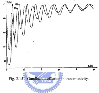
Fig. 2.15 Gundlach oscillation in transmissivity--- 23
Fig. 2.16 Energy diagram for standing waves at high applied bias, which exhibit in the triangular potential in green color --- 24
CHAPTER 3 Fig. 3.1 The whole experiment instrument --- 25
Fig. 3.2 The ion sputter gun used in this experiment, IQE 11 of Specs. (b) Schematic diagram showing a typical ion sputter gun. Such a gun is generally operated with high voltage --- 29
Fig. 3.3 Schematic diagram of ion sputtering for cleansing the sample surface --- 30
Fig. 3.4 Schema showing the structure of an electron-beam gun--- 30
Fig. 3.5 The diagram of the composition of a STM --- 31
Fig. 3.6 (a) When the tip is blunt, tunneling current can be formed from more than one atom and degrade the resolution of the image. (b) If the tip is sharper, the size of the tunneling current is smaller and leads to a better resolution --- 32
Fig. 3.7 The schema of the etching process. Note that “necking” of the tungsten wire occurs at the interface of the electrolyte and the air -- ---32
Fig. 3.8 The schema of the constant current mode of STM --- 33
Fig. 3.9 The schema of the constant height mode of STM --- 34
CHAPTER 4
oscillation of Ag and Au(111) are equivalent to 0.47eV --- 37 Fig. 4.2 (a) STM topography (140nm×140nm) of 1-layer Ag film grown on Cu(111)
surface. (b) dZ/dV-V spectrum of Ag film and Cu(111) substrate.
The separations of Gundlach oscillation are equivalent to 0.32eV --- 37 Fig. 4.3 Schematic of the distribution of standing wave states within a triangular
potential. It shows that the energy separations are due to the difference of the work function between the tip and the sample surface --- 38 Fig. 4.4 (a) STM topography of MgO film on Ag(100) obtained by Schintke et al..
(b) Spectrum of (a). The value of the blue bar is measured as 1.01 eV and supposed to be the correct difference of work functions between the film and substrate--- 40 Fig. 4.5 (a) STM image of faulted and unfaulted Co islands on Cu(111). The image
size is 60nm×60nm. (b) dI/dV-V spectra of faulted and unfaulted Co islands. --- 42 Fig. 4.6 (a) dZ/dV-V spectra of Cu(111) and Co islands. (b) Energy separation for the
two islands--- 42 Fig. 4.7 Reconstructed Au(111) surface with Co deposition at 8K and RT respectively.
Both image sizes are 80nm×80nm --- ---43 Fig. 4.8 (a) The STM topography of single Co atom on reconstructed Au(111) surface.
Three distinct structures in this image are all marked by colored arrows. The image size is 6nm×6nm. (b) STM topography of isolated Co atoms on Au(111) surface --- 44 Fig. 4.9 dZ/dV-V spectrum at higher bias. Energy separations between Co and Au(111)
become constant when the applied bias is close to 7.5V --- 45 Fig. 4. 10 (a) STM topography of Cu(111) with 1ML Ag film in size of 102nm×43nm
acquired in A, B and C indicated in (a). (c) Energy separation as the function of the order for the spectra in (b) --- 47 Fig. 4.11 dZ/dV-V of spectra of Cu(111) with Ag film obtained with various tip
conditions --- 49 Fig. 4.12 Energy separation of the order 0 and 1 as the function of (△E)3/2 for
Ag/Cu(111) system. △E is the energy difference between the order 1 and 2 of Cu(111). The solid lines are the smooth fitting to both data points --- 50 Fig. 4.13 (a) STM topography image of a Ag/Cu(111) surface. The image size is
30nm×32nm (b) The average dZ/dV-V spectra of the hollow and protrusive regions on Ag/Cu(111) surface --- 52 Fig. 4.14 (a) STM topography image of a reconstructed Au(111) surface (286Å×286Å)
(b) The average dZ/dV-V spectra of FCC, HCP and ridge regions --- 52 Fig. 4.15 (a) STM topography image of a reconstructed Au(111) surface. The image
size is 24nm×24nm. (b) dZ/dV-V spectrum acquired on reconstructed Au(111) surface. The first two states are believed as image potential states. (c) Corresponding bias at each apex and valley. (d) Corresponding displacement of the tip at each apex and valley --- 55 Fig. 4.16 (a) Mappings at the apexes of each peak whose biases and displacement are
indicated in Fig. 4.12 (c) and (d). The sizes of these mappings are 24nm×24nm. The contrast in these mappings is opposite to that in STM topography image. FCC regions are brighter than the other two structures --- --- 56 Fig. 4.16 (b) Mappings at the valleys between all peaks, whose biases and
mappings--- 57 Fig. 4.17 Dependence of the possible resolution on the increasing tip-sample gap width
INTRODUCTION
Quantum size effect (QSE) is a description for the physical properties of materials, directly affected by energy level splitting, surface effect, or energy band gap. This phenomenon only occurs when the scale is smaller than μm. In recent 20 years, one of QSE studies, surface effect has attracted much attention since Binning et al. utilized STM to observe the reconstructed Si(111) surface[1-1]. STM has become one of the efficient methods to obtain the electronic and geometric structure of the observed surface. Besides surface topography, STM is also used as scanning tunneling spectroscopy (STS) to show the dependence of tunneling current as well as tip-sample displacement on ramping bias. By STS, we can realize the local electronic states exhibiting within the tip-surface gap. Jiutao Li et al. have utilized STM to find the standing wave states on Ag(111) surface[1-2]. The low voltage peaks or shoulders are assigned to the properties of these states.
For the high-voltage peaks, the influence of field emission resonances on the transmission probability has been first simulated by K. H. Gundlach and is also called Gundlach oscillations[1-3]. Afterwards, S. Schintke[1-4] et al. and M. Pivetta[1-5] et al. have also tried to estimate the work function of thin film system by Gundlach oscillation performance measured by STS in Z-V mode. In former reports, the work function difference is considered as the energy separation of the first peak in the spectra. However, we observed that the energy separations of higher order peaks are constant. We try to explain the physical meaning of the constant separation in this thesis. In addition to uniform ultrathin film system, we also tried to find the energy separation between distinct films and substrate. Pendersen have observed the specific
and unfaulted, and are defined due to their different surface energy. These two Co islands has been studied by O. Pietzsch et al. by dI/dV-V spectrum[1-7]. Since the energy separation is attributed to the electronic structures difference, the energy separations between the two islands and substrate are supposed to be unlike each other. Here we find the distinct energy separation and see whether the two structures can be classified by dZ/dV-V spectra.
Moreover, Madhavan et al. have observed that single Co atoms are about 12.3Ǻ on a reconstructed Au substrate.[1-8] Based on this observation, we can have Z-V measurement on single Co atoms (about 12Å) and find out whether single atoms have contribution to the work function difference.
During the scanning process, we have found that there may exhibit discontinuous contrasts in the STM images. The discontinuous image is referred to the change of tip condition. The change of the tip shape is accompanied with the variation of the electronic field between the tip and the surface. Kubby et al. have calculated the electronic field between the tip and sample surface by dZ/dV-V spectra.[1-9] Here we can have the exact tip-sample field from Kubby’s formula and find whether the energy separations vary with tip condition and tip-sample electric field as well.
Recently W. Chen et al. have demonstrated that the electronic structure of HCP region is different from that of FCC[1-10]. W. B. Su et al. have shown that the electronic characteristics of the three structures on reconstructed Au(111) surface are distinct[1-11]. They implied the transmissivity of the distinct structures is slightly different and the complementary phenomenon in energy was also observed in the distinct structures. These two phenomena have also appeared for Ag/Cu(111) system. Based on the different intensity of distinct structures, we can obtain differentiating STM image during Z-V measurement. The differentiated images provide information about the
tried to obtain clear differentiated images with a far tip-sample distance. If we can have image resolution better than 1nm when the tip is several nm from the sample surface, we should have a technique to analyze some soft material. The technique is applicable in the observation of carbon nanotube (CNT) and DNA. However, due to the small size of CNT and DNA (<1nm), the observed objects may be taken by the tip during the scanning because the tip-sample distance is usually within 1nm. During the Z-V measurement, the tip-sample distance is increasing with the enhanced applied bias. Hence we also tried to obtain the surface topography with the tip-sample distance as far as possible. While the tip is far away from the sample, the image we obtained also represents the resolution we could have.
C
H A P T E R
2
THEORY
2.1 Surface Science
Since 1960, surface science has undergone great development on the basis of many concepts such as vacuum theory, quantum effect, and Crystallography. The main distinct feature of modern surface science is to deal with crystal surface, which is well-defined in structure and composition. In other words, even for the same material, difference in the lattice structure may lead to great divergence in properties. Therefore the selection of the structure of substrates is as important as that of the substrate material in surface science.
Metals and semiconductors are both popular as being substrates. When it comes to solid surface, one conventionally means the outermost atoms on the topmost few layers, i.e., within the region of 100Å in depth, whose atomic arrangement and electronic properties are substantially different from those of the bulk. Observation of atomic arrangement on the surface of metals and semiconductors is pretty interesting due to the specific phenomenon, reconstruction and relaxation, which will be introduced in detail in section 2.2.
Generally we can divide the surface study into two parts, adsorbates-free and adsorbates-covered. In the case of adsorbate-covered surface, the amount and material of the adsorbate both have great influence on electronic or magnetic properties. Those performances also differ with the location of the adsorbates and their aggregation behavior on the substrate, i.e. film growth. Mechanism of adsorption and film growth is quite simple and will be interpreted in section 2.3.
2.2 Structure of Clean Surface
The atomically clean substrate surface is necessary for the most studies in surface science, and therefore knowledge of the atomic structure of clean surface is of great importance. The general modifications of surfaces are relaxation and reconstruction which can occur on either metal or semiconductor surfaces[2-1].
When an infinite crystal is broken along a certain crystallographic plane and forms a semi-infinite crystal, due to the absence of neighboring atoms on one side, the surface atoms are modified to reduce its surface energy. Hence, the equilibrium structure of the topmost layer differs from that of the corresponding atomic arrangement in the bulk.
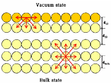
2.2.1 Surface Relaxation
When the atomic structure of the topmost layer is the same as in the bulk but the first interlayer spacing is modified, the “normal relaxation” is defined and shown in Fig. 2.1. It can be seen that the spacing between the first two layers is contracted and results in the extension of the second spacing.
The variation of the spacing is due to the stress equilibrium. We can observe that atomic spacing in the bulk is balanced by the symmetrical set of forces. On the other hand, the atoms on the unrelaxed surface suffer an imbalanced force that may pull them toward the second layer and shrink the first interlayer spacing d12 . The
Fig. 2.1 Schematic of internal force during relaxation in top layers.
In most cases, normal relaxation occurs in metals. In addition to normal relaxation, sometimes there is also another model that uniform displacement of the surface atoms parallel to the surface occurs. The case is defined as tangential relaxation and appears mainly at high-index surfaces with low atomic density.
2.2.2 Surface Reconstruction
In most cases when it comes to the modification of the surface, it refers to “reconstruction.” The symmetry and periodicity of the reconstructed surfaces are different from those of the bulk. Depending on whether the number of atoms on the top layer is preserved or not, there are two types of reconstruction named “conservative reconstruction” and “non-conservative reconstruction.” By the literal meaning it is explicit that the former maintains the number of atoms while reconstructing and only the displacement of surface atoms is involved in. On the contrary, in non-conservative reconstructions, the number of atoms on the reconstructed layer is changed in comparison with the bulk. In other words, the total number of atoms in the reconstructed layers is not equal to the number of atoms in an
integer number of bulk layers.
Reconstructions occur not only for a limit number of metal surfaces, such as Au and Pt, but can also be seen in ultrathin film systems. The main feature of reconstruction is the specific structure on the surface. Only when the unique topography of the surface is observed, the reconstruction is considered to be done. In this thesis, there are two reconstructions observed on Au(111) surface and Ag film on Cu(111) surface respectively. Here goes the brief introduction of the two systems.
a. Au(111)
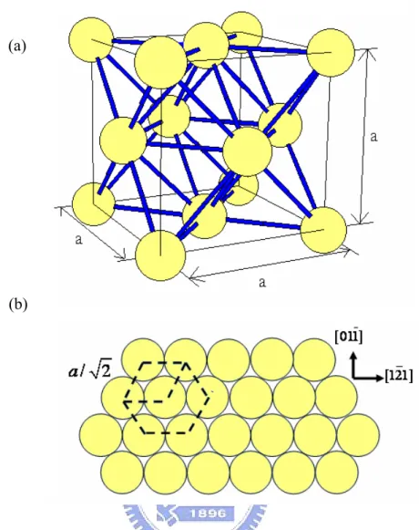
Some noble metals such as Au, Ag, and Cu, have the face-centered cubic (FCC) crystal structure as shown in Fig. 2.2 (a).
However, gold is the only FCC metals that has a reconstruction of the closest- packed (111) surface. This unique phenomenon has been observed by means of low-energy-electron-diffraction (LEED)[2-2]、transmission electron microscopy (TEM)
[2-3] , and in recent years, scanning tunneling microscopy (STM). When an Au bulk is
cut along the (111) plane, as shown in Fig. 2.2 (b), a unique twofold symmetry, (22× 3) “herringbone reconstruction” appears. The reconstructed Au (111) surface consists of higher concentration of Au atoms than that in the underlying layers because of its 4.4% contraction along [011] direction on the surface layer. The compression along [011] results in the separation of surface atoms into two kinds of arrangment: some occupy normal FCC sites and others are at the hexagonal-close packed (HCP) sites[2-4].
Fig. 2.2 (a) FCC unit cell with the lattice constant a=4.08Å of Au.(b) The (111) face of FCC.
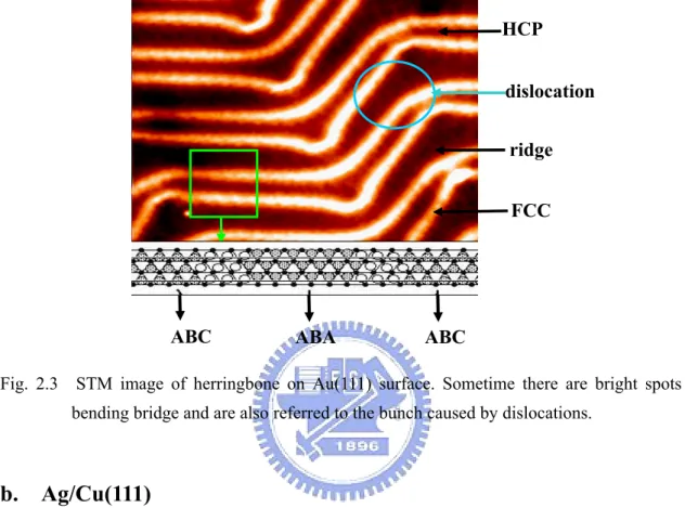
This compression is resulted from the formation of stacking fault on the surface. The unfaulted stacking (ABC packing, FCC structure) and the faulted stacking (ABA packing, HCP structure) are separated by the bridge rows schematically shown in Fig. 2.3. The HCP regions are slightly smaller in size than FCC regions because HCP regions possess slightly higher energy[2-5].The transition regions, the bridge rows, tend to have a smaller nearest neighboring distance (2.68Å) while that in the FCC regions are relatively larger (2.86Å)[2-6].
The specific long-term ordering reconstruction of Au surface is believed to exhibit significant internal strain. In other word, local defects can be expected to sensitively impact the reconstruction pattern in the surface layer.
(a)
Fig. 2.3 is the reconstructed Au surface observed by STM image. It is clear that the bridge rows (bright regions) bend symmetrically on the surface. It is because strain-stabilized screw dislocations exist and lead to surface stress release.
Fig. 2.3 STM image of herringbone on Au(111) surface. Sometime there are bright spots on the bending bridge and are also referred to the bunch caused by dislocations.
b. Ag/Cu(111)
Besides the surface of a bulk, reconstruction also occurs in the system of thin film. When the parameter mismatch between the adsorbates and substrate exhibits, the immiscibility and interfacial strain are inevitable. In order to release the interfacial stress, reconstruction occurs and usually goes along with specific superstructures.
One of the representative superstructure in thin film system is Ag/Cu(111). When the coverage of Ag film is less than 2ML, a well-known superstructure n×n can be observed by means of low-energy electron diffraction (LEED)[2-7] and scanning tunneling microscopy[2-8]. This superstructure arises from the commensurate lattice constant of Cu(3.61Å) and Ag(4.09Å), i.e. 37.6% as the lattice mismatch. The large mismatch leads to great stress and strain in the interface of Ag/Cu(111). To release the
FCC ridge HCP
dislocation
interfacial stress, there comes partial dislocation loops in the top layer of substrate with the removal of some Cu atoms. These Cu atoms move from the original FCC sites to HCP sites[2-9], shown in Fig. 2.4 (a). The FCC-to-HCP shift offers stable triangular hollow sites for the overlayer Ag atoms. In 9×9 superstructure, shown in Fig. 2.4 (b), is 4 or 5 atomic row wide with 1, 3, or 6 atoms protruding in the center. The amount of n varies with the elaboration temperature. If the film deposition is followed by annealing, 9×9 superstructure will be the most favorable.
Such reconstruction can be observed in Au/Ni(111) system as well. A monolayer of Au film on Ni(111) surface also results in ordered array with triangular dislocation loops. This kind of superstructure is also called Moiré pattern, which is ascribed to the combination of two different structures. However, this phenomenon only exhibits when the film is thin enough to differ from bulk state.
Fig. 2.4 (a) Structural diagram shows the triangular misfit dislocation. (b) STM topography of the 9x9 superstructure of Ag/Cu(111).
2.3 Film Growth
In surface studies, attachment of different species on clean reconstructed surface (a) (b)
is also of great interest. The added species are called “adsorbates,” which may attach on the surface in two ways, either physisorption or chemisorption. These two adsorptions are subdivided depending on the strength of interaction between an adsorbate and a substrate. While the number of the adsorbates is large enough to cover part even all the surface of the substrate, “thin film growth” is defined. Growth mechanism of thin film deserves a detailed discussion following the introduction of simple adsorption[2-10].
2.3.1 Adsorption
Physisorption is the case that the interaction between an adsorbate and a substrate is considered as the weak van der Waal forces. The physisorbed atoms or molecules can never disturb the original structure of the substrate. This kind of adsorption can only be detected when the chemisorption is absent and the substrate temperature is low enough. An example of physisorption is the adsorption of noble-gas atoms on metal surfaces at low temperature.
On the other hand, chemisorption takes place when strong chemical bonds are formed between the adsorbates and the substrate. Interaction of chemisorption between the adsorbates and the substrate is much stronger than that of physisorption. It is also the reason why physisorption can only be detected without chemisorption. Adsorbates of chemisorption can usually dissociate or form new adsorbate species such as magic islands or small clusters. The structure of the substrate is also changed because of the addition of adsorbates in the way of relaxation or reconstruction. In such cases, thermal activation is inevitably desired. An example of chemisorption is the adsorption of metal atoms on metal or semiconductor bulks at varying temperature. In our system, deposition of silver film is the case of chemisorption.
2.3.2 Thin Film Deposition
Deposition of thin film takes place on the premise that nucleation sites are found and the adsorbates are stabilized on the substrate. Adsorbates emitted from the sources such as electron-beam evaporators or K-cell effusion sources, are able to attach on the surface through the exchange of kinetic energy with the sample. Growth of thin film is divided into four processes in order:
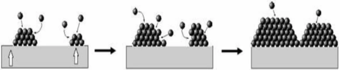
a. Nucleation
Adsorbates arriving to the substrate are desired to stay on the surface for a period of time instead of stop acting. These gaseous adsorbates release superfluous energy and condense on the surface as several steady clusters, as seen in Fig. 2.7(a). While a cluster is smaller than the critical size, called an “embryo,” the surface energy is dominant and the free energy is positive, hence the embryo is momentarily intended to shrink or disappear. On the contrary, if the cluster is larger than the critical size, called “nuclei,” the volume free energy is prevailing and the cluster tends to grow into a greater one to decrease its total free energy.
The nucleation process can be manifested by the thermodynamic formula:
( 2-1 )
where
Δ
G
is the total free energy,Δ
G
v the unit volume free energy which is anegative value,
γ
the unit surface energy which is always a positive value, and r the radius of a cluster. The relationship of energy versus cluster size (radius r) is shown in Fig. 2.5, where r* is the critical radius of the cluster. Unless the clusters are large enough to attract more adsorbates, they can never grow in size and become the desired film structure. 3 24
G
4
3
π
r
G
vπ γ
r
Δ
=
Δ
+
Fig. 2.5 Energy diagram during the nucleation process.
b. Grain Growth
After nucleation completed, a cluster can grow stably and adsorb more gaseous atoms onto itself, as shown in Fig. 2.7(b). This process is considered as the sign of the starting of film growth. The driving force of this process is attributed to the decrease of total free energy △Gr. During this process the adsorbates are actively attaching on the
clusters to reduce the volume free energy and make the system steadier. c. Coalescence
When the clusters grow larger and are able to connect to each other, as illustrated in Fig. 2.7(c) and (d), inter-diffusion within these clusters occurs and comes along the linkage of these bunches. The clusters merge with each other in consequence and become larger and steadier, referred to “coalescence”.
d. Film Growth
After the coalescence of clusters, channels between these bunches are filled up and the model of a thin film thereby appears, as shown in Fig. 2.7(e). There usually
3
4
3
π
r
Δ
G
v 24 r
π γ
* G *r
rG
exhibit many volume defects such as steps and kinks (Fig. 2.6) on the film surface. Adsorption is more complicated on these three-dimension structures formed on the thin film than that on a clean substrate. In general, chemisorption tends to take place on these defects in order to reduce the surface energy. In other words, processes mentioned above are not the only possible ways to evolve a wanted film.
Fig. 2.6 Diagram of the possible nucleation sites.
2.3.3 Thin Film Models
Generally speaking, thin film growth is divided into three modes:
I. Frank-Van der Merwe mode(F. M. mode)
Monolayer-by-monolayer growth only occurs in F. M. mode (Fig. 2.8). It can be seen as a two-dimension growth. However, the internal strain induced by the interfaces increases with thickening of the film. The layer-by-layer growth condition is usually seen when the lattice mismatch is quite small (< 10%)[2-10] so that there are little stress on the interface.
Fig. 2.8 Schematic of monolayer-by-monolayer growth for Frank-Van der Merwe mode.
II. Volmer-Weber mode (V. W. mode)
When the adsorbates gather in three-dimension and become islands, we call the growth condition V. W. mode, illustrated in Fig. 2.9. V. W. mode usually occurs when the lattice mismatch is high.
Fig. 2.9 Schematics of islands growth for Volmer-Weber mode.
III. Stranski-Krastanov mode(S. K. mode)
After the formation of several monolayers, three-dimension islands appear to accommodate the lattice mismatch. In other word, islands are formed above these monolayers. This growth mode is called S. K. mode which is the combination of F. M.
mode and V. W. mode, shown in Fig. 2.10. This mode is the prevailing when the lattice constants and structure of the film and the substrate is similar.
Fig. 2.10 Schematic of mixed growth for Stranski-Krastanov mode.
2.4 Scanning Tunneling Microscopy
Scanning tunneling microscopy has become one of the most powerful surface analysis technique since its successful performance taken by Binnig and Rohrer at the IBM Zürich Research Laboratory in 1981[2-11]. The main mechanism used in this technique is “tunneling effect” and the “spectroscopy.” Both the mechanisms can only be accomplished on the basis of quantum effect. Thus in this section they are described in brief and shows the physical principle of the STM. Figure 2.11 illustrates an easy model of an STM with its fundamental compositions and shows the mechanism to sketch the topography of the sample surface.
2.4.1 Tunneling Effect
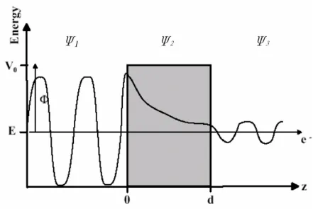
Tunneling of electrons is a quantum mechanical effect that allows electrons to penetrate through a potential barrier. It is the most important feature among all theories used in a STM. To explain the tunneling effect, the Schrödinger equation for one-dimensional regular potential has to be solved,
2 22 ( ) ( ) ( ) ( ) 2 d x V x x E x m dx ψ ψ ψ − h + = (2.2) where Ψ(x) is the wave function of the electron, V(x) the potential of barrier, E the
energy of electrons, m the mass of particle,h the reduced Planck constant. The solution derived from the Schrödinger equation can be shown as follows:
ψ1= ikz ikz Ae +Be− (z < 0) ( )x ψ = ψ2 = z z Ceκ +De−κ (0 < z < d) (2.3) ψ3= ikz Fe (z > d) in which k = 2mE h , κ= 2 (m V −E)
h , and is schematically shown in Fig. 2.12.
As we can see, electrons with energy E still have possibility to penetrate the constant potential barrier Vo even though Vo >E. To make it simpler, A=1 is assumed
and it can derived that
C= 2 2 1 k κ − , D=2ik κ , and 2 2 2 2 (1 )sinh( ) cosh( ) i d ik F e k ik d kd κ κ κ κ κ − = − −
From the general solution, the transmittance can be shown as
2 2 2 2 | | d exp 2 m( ( ) ) T ≈e−κ = ⎧⎪⎨− V x −E dx⎫⎪⎬ ⎪ ⎪ ⎩
∫
h ⎭ where 2 2 ( ) m V E κ = − h (2.4)Once the transmission occurs, the tunneling can be given in the following way: 1( ) (2 )[ ( ) ( )]
where f( )ε is the Fermi-Dirac distribution, which is the average occupation number of state of energy. n1( )ε and n2( )ε are density of state in the vacuum region between
the sample and the tip. Another approximation of the tunneling current can also be shown as: 2 2 | (0) | F E kw T n E eV I ψ e− − ∝
∑
(2.6)where U is the applied bias between the sample and the tip, and Φ the average work function. Thus no tunneling current can occur without external bias. The applied voltage determines whether the standing wave states or the local density of states will contribute to the tunneling current.
Therefore, | |2
T decreases exponentially with d, the distance between the tip and
the sample surface, and the tunneling current decays with d as well. 2.4.2 Density of State
STM is able to measure the local density of state (LDOS) of a material surface as a function of lateral position. When it comes to an individual electron, it has a specific energy level. It means that only certain electrons with the specific energy can occupy the given energy levels. The distribution that makes electrons (in the tunneling current) allow each energy state as a function of applied energy between the tip and sample is the so-called density of state, DOS(E). DOS(E) is the quantity dependent on energy[2-12].
Furthermore, DOS (E) can also define the local density of state, LDOS(E), as the quantity of the energy level dependent on the energy and on the particular position. In other words, LDOS (E) is the density of electrons of certain energy at the specific spatial location. We can express the LDOS as ρs ( , )z E :
2 1 ( , ) | ( ) | E s E z E z ε ρ ψ ε − =
∑
(2.7) Take (2.5) into consideration, tunneling current is proportional to the LDOS:1.025 2
(0, ) kw (0, ) w
s F s F
I∝Vρ E e− ≈Vρ E e− ϕ (2.8)
Besides topography, we can also obtain the electronic property of the sample surface by using scanning tunneling spectroscopy. The tunneling current is measured from the variation in the bias voltage between the tip and the sample surface so that we can obtain the I-V curve or the differential conductance-voltage (dI/dV)-V curve. From both curves mentioned above, we can obtain the information of the local density of state of the sample surface, and the LDOS can be given by following approximation:
0 ( ) ( )
eV
s t
I ∝
∫
ρ E ρ −eV +E dE (2.10)where ρ is the LDOS of the sample surface, and s ρ the LODS of the tip. Because t
the tunneling current only continues until the Fermi levels of both conductors are equal. Thus dI/dV can be expressed as follows under the assumption that ρ is constant t
within the measurement:
( )
s F
dI
E eV
dV ∝ρ − (2.11)
Consequently, the dI/dV is proportional to the LDOS, which means when the density of states is higher, the more likely it is to form desired tunneling current under the same applied voltage.
Fig. 2.12 Tunneling of a single electron through a one-dimension rectangular barrier with constant potential Vo.
2.5 Scanning Tunneling Spectroscopy
Besides providing topography of the sample surfaces, the STM can also perform spatially localized tunneling spectroscopy. Without applying bias on the tip, the Fermi level of the tip and the substrate surface are equal. Under such circumstance, no tunneling current appears because there is no energy difference between both sides. However, applying different bias on the tip can lead to the variation of the Fermi level of the tip and the spectroscopy performs its specific characteristics under different applied bias. When the tip bias is negatively applied, the Fermi level of the tip is raised and electrons are more likely to transmit the vacuum gap from the tip to the substrate. On the contrary, electrons can flow through the gap from the substrate when the tip bias is positively applied. Thus the sign of the tip bias determines the direction of the tunneling current. Furthermore, the intensity of the applied voltage is significant to the behavior of electrons as well.
Here we will discuss the physical meaning of the spectrum obtained at low and high biases.
t
φ
( ) F tE
e
-( ) v sE
( ) v tE
( ) F sE
sφ
2.5.1 At Low Bias: Surface State ( Bias<Φ)Electron band theory of solids bases on the existence of the states of allowed energies, which are separated by specific band gaps. For the one-dimensional problems, the potential associated with an infinite crystal proposed by Schrödinger can be simplified in two forms, bulk states and surface states.
The bulk states are wave functions extended into the bulk and decay exponentially into the vacuum, and the surface states are that localizes around the surface region decaying with exponentially into both bulk and vacuum. These surface states are constrained within the gap, is also called true surface states when they are located within the gap of the projected bulk bands. The states settled on the energy levels of the bulk bands are considered as surface resonances.
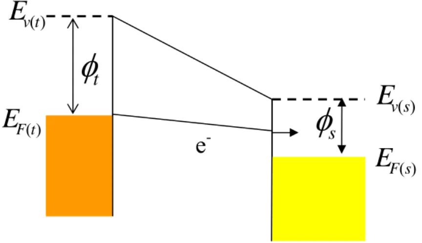
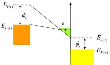
The surface states above are termed intrinsic surface states that denote themselves to characterize the electronic structure of ordered crystal surface in its ground states. Surface states are usually obtained at low bias due to the low energy they possess. Fig. 2.13 shows the tunneling occurring at low tip bias, where Φs and Φtstand for the work function for the sample and the tip respectively.
Fig. 2.13 Schema of electrons performance at low tip bias. The tunneling electrons transmit through the rectangular potential and are confined below the vacuum level of the sample.
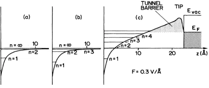
There are other surfaces states originating from the perturbation of the surface potential, such as extrinsic surface states and image potential states. Image-potential states refer to the surface states induced by the electrostatic interaction of electrons with its image charge in the surface. The electron above the metal surface repartition the charge in the bulk and an attraction is thereby formed. The energy of image potential states is lower than that of vacuum level as shown in Fig. 2.14, where n=1 is the image potential state[2-13]. While a bias is applied, the energy level expands over the vacuum level and a triangular potential appears. The image states can be shifted. The image potential states are localized in vacuum with several Å away from the metallic surface.
Fig. 2.14 (a) For simplicity, only n=1 and n=2 hydrogenic energy levels are shown. (b) The surface corrugation pulls the energy level down. (c) Expansion and shift of image potential states with an applied bias.
2.5.2 At High Bias: Gundlach Oscillation ( Bias>Φ)
When the tip bias exceeds the work function of both electrodes, i.e. the Fermi level of the tip is raised above the vacuum level of the sample, rectangular potential barrier become triangular and electrons with energy E are able to tunnel from the tip and transmit through the triangular potential well, shown in Fig. 2.16. When the
electrons are biased to specific energy, they are able to tunnel the triangular potential and trapped at the states within the potential. Transmissivity of these electrons is nearly 1 and result in standing wave. The intensities of the standing wave states oscillate with bias variation. This phenomenon was observed by Gundlach2-12 and also called Gundlach oscillation[2-14](Fig. 2.15).
Fig. 2.15 Gundlach oscillation in transmissivity.
Gundlach oscillation can be observed by Z-V spectroscopy. With an active feedback and fixed tunneling current during the Z-V measurement, the tip moves from the surface when the bias is ramping (usually 2V to 9V). The movement becomes faster when the tunneling current strengthens suddenly, i.e. at which bias a standing wave states exhibits. Hence we can know the states by differentiating the Z-V spectrum, in which the positions of the peaks stand for the states energy. Usually the intensity of the states decays when the bias gets higher, i.e. the displacement of the tip becomes larger.
Fig. 2.16 Energy diagram for standing waves at high applied bias, which exhibit in the triangular potential in green color.
t
φ
( ) F tE
e -( ) v tE
( ) v sE
( ) F sE
sφ
EXPERIMENTAL SETUP
3.1 Experiment Instrument
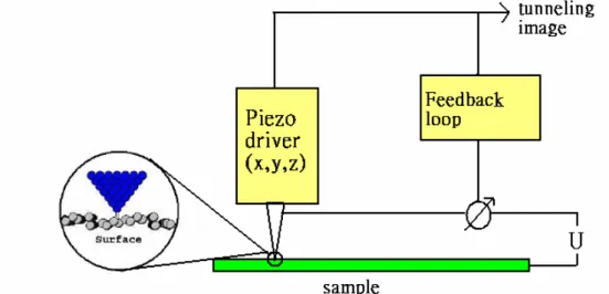
This experiment is performed in an ultra-high vacuum system consisting of a low temperature scanning tunneling microscopy (LT-STM) and a designed preparation chamber. To avoid the thermal disturbance, the STM is cooled to 4.3K by liquid Helium set upon it. The entire equipment is illustrated in Fig. 3.1. In this section, the ultra-high vacuum system will be described first followed by the preparation of the Au sample. The important parts of the STM will also be introduced in detail.
Fig. 3.1 The whole experiment instrument.
Cryostat STM Gauge Preparing Chamber Ag Electron-beam Evaporator Co Evaporator Vibration Isolation
The most important purpose of the ultra-high vacuum system is to keep the sample surface clean for a sufficiently long time. The “monolayer time” (the time it takes to contaminate the surface with a single layer of molecular adsorbates ) can be approximated as:
t = 3.2 x 10⁻⁶ /P (3.1)
where time t is in seconds and pressure P in millibar. By the formula it can be seen that the lower the pressure is, the longer time it takes to contaminate the sample surface. Hence we keep the pressure under 10−8 mbar to ensure the sample being clean. To achieve the desired vacuum, we use four pumps step by step[3-1].
3.2.1 Mechanical Rotary Pump
A mechanical vacuum pump is also called a “Forepump” because it can start in the air (the working background is about 760 torr ~ 10-3 torr) and is the foremost step in the ultra-high vacuum system. A mechanical pump physically “compresses and sweeps” the air molecules from the system with an inside rotary. Compression of the air during pumping may lead to condensation of vapor in the pump exit. Thus the more air is swept away, the more vapor is condensed in the exit leading to the reduction of pumping efficiency. Generally there is a “gas ballast” set insides to prevent sweeping improper gas which may condense into liquid phase.
3.2.2 Turbo Molecular Pump
A turbo molecular pump is a type of vacuum pump used to obtain and maintain intermediate pressure lower than 10-4 torr. Turbo molecular pumps works on the principle that give certain momentum to the gaseous molecules in a desired direction by repeating collision with rotating vanes, and the gas can be exhausted to keep the
easily injured by the collision with the strong flux of gaseous molecules, thus the chamber has to be pre-evacuated when the turbo molecular pump starts. The working background of a turbo molecular pump should be 10-3 torr ~ 10-10 torr.
3.2.3 Baking
It cannot be possible to achieve the desired ultra-high vacuum if the chamber is treated only by pumping. In this experiment we always baked out the chamber up to 120℃ and running the rotary and turbo molecular pumps simultaneously to remove contaminants such as H2O、CO2 from the chamber wall. Usually we keep baking for 48
hours to assure the evacuation of vapor. 3.2.4 Ion Pump
After the former two pumps, the lowest pressure is approximately 10-9 torr without further treatment. To achieve lower pressure (usually in the 10-10 torr degree), an ion pump is necessary. An ion pump is operated by ionizing gas within a magnetically confined cathode made of Titanium. It can entrap electrons on the spiral route by an external magnetic field in order to increase the possibility to collide with ionized gas. Gas cations in the chamber will crash into the cathode (Ti board) and sputter the Ti out which may lead to Titanium gettering of active gas as well as burial of gas into the chamber wall. Burial is the basic mean of pumping heavy noble gas. Hence ion pump is efficient enough to obtain ultra-high vacuum.
3.2.5 Titanium Sublimation Pump (TSP)
A titanium sublimation pump is operated intermittently to assist the ion pump maintaining ultra-high vacuum. The working principle is very similar to ion pump, and
while working, and extend the lifetime of the ion pump. Though the working background of a TSP is about 10-4 torr ~ 10-12 torr , it is usually started under the pressure lower than 10-7 torr .
3.2.6 Ionization Gauge
Operation of an ionization gauge is an indirect method to detect the accurate pressure. Under ultra-high vacuum, the mean free path of gas molecules becomes larger than that in the atmosphere. If the gas in the chamber is ionized to be ion current and detected, it is capable to calculate the amount of gas molecules in the chamber. We use the “Hot-cathode” ionization gauge, PERKIN ELMER DGC III, in our experiment in which the hot electrons are generated from the tungsten filament and are accelerated by an external electric field. Gas molecules are ionized by the bombardment with these hot electrons. The working range of hot-cathode ionization gauge is limited to 10-2 torr ~ 10-11 torr.
3.3 Sample Preparation
In former chapter, we have mentioned the Au reconstruction. Because the main purpose of this experiment is to know the quantum effect on the Au surface such as standing wave states and surface states, which can only be known on the contaminants free substrate, hence the surface cleansing is quite significant. To obtain the specific reconstruction of Au(111) and clean Cu(111) surfaces, two steps are needed[3-2].
3.3.1 Ion Sputtering
Surface contaminants can be sputtered off the host atoms on the topmost layers by bombardment of the surface by energetic noble gas ions. The source of the ion beam
system) filament inside the UHV chamber (Fig. 3.2). It clearly shows that electrons emit from the cathode, also the metal substrate. Thereby the ionized gas atoms, Ar+, are attracted toward the sample with a given acceleration[3-3].
Fig. 3.2 (a) The ion sputter gun used in this experiment, IQE 11 of Specs. (b) Schematic diagram showing a typical ion sputter gun. Such a gun is generally operated with high voltage.
3.3.2 Annealing
Annealing is a heat treatment in which the substrate that exposed to an evaluated temperature environment for a period of time and cools down slowly. The purpose of annealing is to relieve the internal stress, produce the specific well-ordered microstructure and remove the residual Ar+ ions, as shown in Fig. 3.3. Generally the required annealing temperature is much lower compared to the one when only heating is needed. The annealing temperature is pretty critical and the process is theoretically accelerated with increasing temperature. Besides the desired temperature, holding time is also an important parameter in the procedure. After heating and holding, if the cooling rate is too fast, it is possible to induce other internal stress and results in warping even cracking. In practice, several cycles of ion sputter/annealing are
3.3.3 Electron Beam Gun
In our system, deposition of silver film is executed with the electron-beam gun. Its structure is shown in Fig. 3.4. When the filament is heated, hot electrons are generated and accelerated toward the crucible which is filled with the source, silver. The bombardment results in the warming up of silver. Therefore gaseous Ag ions emit from the bulk and attach onto the sample which is negatively biased. By controlling the emission current of electrons, we can know the ion flux of Ag ions sent out and the deposition rate can be stabilized. This method is an efficient way to control the amount of deposition.
Fig. 3.4 Schema showing the structure of an electron-beam gun.
Shutter controlling shaft
High voltage Cooling Current Shutter Filament High voltage Insulating ceramic
An STM is basically composed of a probe, a scanner, a stepper and a vibration isolation system. In this experiment we also add a cooling system to maintain the STM cool as 4.3K. In the following articles these elements will be introduced in detail. The composition of the STM is clearly shown in Fig. 3.5[3-4].
Fig. 3.5 The diagram of the composition of a STM..
3.4.1 Tip
The sharpness of the probe tip determines the resolution of the STM image. If the tip is blunt, which means a cluster of atoms are packing closely on the surface, it will blur out the image because tunneling current will be formed from many atoms. When the tip is sharper, tunneling current are likely to emit from the topmost single atom, which can be understood from Fig. 3.6. Electric field between the tip and the substrate surface also varies with the sharpness of the tip. In general, with identical applied bias, the field within the tip-sample gap is stronger when the tip is blunt. Tunneling current is hardly generated from a blunt tip because atoms on the tip need higher external voltage to emit electrons and maintain at the desired current intensity.
Outer shielding
Tip Scanner Stepper
polishing the wire surface to remove the oxide outside, we apply a voltage with potential 5 V between the tungsten probe (as a positive electrode) and platinum (as a counter electrode). Both electrodes are set in a 5M KOH solution as electrolyte during the etching process. As far as the etching goes, tungsten at the interface of electrolyte and air becomes so thin that breakage occurs due to the weight of the bottom part of the wire. The process of etching terminates when the wire breaks down. It can be illustrated in Fig. 3.7.
Fig. 3.6 (a) When the tip is blunt, tunneling current can be formed from more than one atom and degrade the resolution of the image. (b) If the tip is sharper, the size of the tunneling current is smaller and leads to a better resolution.
Fig. 3.7 The schema of the etching process. Note that “necking” of the tungsten wire occurs at the interface of the electrolyte and the air.
As mentioned above, topography of the sample surface is measured by means of detecting the tunneling current. By applying bias between the tip and the sample (with the distance within 10Å), the electrons are able to penetrate the vacuum barrier and form the tunneling current, as shown in Fig. 2.13 and Fig 2.14. The sign on the bias determines either the filled states or the empty states we measure. If the bias is positively applied to the tip, the surface of the sample is regarded as empty sate and tunneling current flows from the tip (occupied state) into the sample (empty state). On the contrary, tunneling current can flow from the sample into the tip when the bias is negatively applied to the tip.
There are mainly two techniques for STM operation. I. Constant current
When scanning the sample surface, the scanner keeps the tunneling current constant by feedback circuit. Therefore the vertical motion of the tip reflects the topography of the surface, as shown in Fig.3.8. This mode is the most widely used technique for desired STM images. For an electronically homogeneous ideal surface, constant current means constant gap between the tip and the sample. This mode is highly sensitive to the geometry of the surface.
In the constant height mode, the tip travels on a horizontal plane above the sample and the tunneling current varies with the topography and local properties of the sample (Fig. 3.9). The factor fixed in this mode is the tip bias, and the tunneling current is measured at every location in order to depict the topography. Generally the scanning speed in this mode is faster than that in the constant-current mode. However, this mode is practicable only when the surface of the plane is relatively flat to keep the tip from crashing.
Fig. 3.9 The schema of the constant height mode of STM
3.4.3 Scanner
Scanners of a STM are mostly made of a piezoelectric ceramic material used to raster the tip over the observed area on the sample surface. By applying electric signals of 1 mV to 1 kV the piezoelectric material is able to induce an electric field inside and makes a little change of its structure and dimensions. A piezoelectric scanner is used here to convert the given signals into mechanical motion in the range of Å to several μm.
3.4.4 Vibration Isolation
For stable operation of the STM, external disturbance should be avoided as well as possible. To reduce the change between the tip-sample separations caused by
vibration is prevented with the interaction of the induced Eddy current in the magnetic field of the permanent magnets mounted on the outside stage and the cooper plates attached on the inside stage.
3.4.5 Low temperature environment
In our experiments the low temperature environment is maintained by a cryostat set upon the STM. We fill liquid He into the cryostat to keep the temperature around 4.2K. The purpose of low temperature environment is to reduce the thermovibration during scanning process. Both the STM and the sample are isolated by multi-shielding so that the thermal drift during the operation is within 2Å per hour.
RESULTS & DISCUSSION
4.1 Energy Separation Measurement
As mentioned in chapter 2, we can understand several physical phenomena by Z-V measurement, including Gundlach oscillation, the energy of image potential states and standing wave states. In thin film systems, spectra of the film and substrate must differ from each other because of their different geometric or electronic structures. In this section the physical meanings for the difference in spectra and the influential factors have been discussed.
4.1.1 Energy Separation in Uniform Ultrathin Film System
The substrates we selected were reconstructed Au(111) and Cu(111). Both samples were cleaned with argon-ion bombardment followed by annealing at 600℃. Ag atoms were deposited on reconstructed Au(111) and clean Cu(111) surface respectively through electron-beam evaporator with the deposition rate of 0.3ML/min. In both Ag/Au(111) and Ag/Cu(111) systems, the Ag films are uniform and grow in layer-by-layer mode. We took the Z-V spectra of one-layer Ag film and the substrates, and the morphology was observed by the homebuilt STM kept at 4.3K.
Fig. 4.1 shows the dZ/dV-V spectrum acquired on a reconstructed Au(111) surface with one-layer Ag film. Both Ag film and the reconstructed Au(111) substrate are marked by green arrows. The distinct peaks marked by numbers (Fig. 4.1(a)) are referred to the standing wave states for Au(111) and Ag film respectively. It is interesting that the peaks at higher energy for the same order are both at a constant separation of 0.47 eV.
film, which are marked by green arrows. Here we can directly classify the same order standing wave states of Ag film and Cu(111) respectively, marked from 1 to 5. We also observed that the constant separations between Ag and Cu(111) is 0.32 eV.
Fig. 4.1 (a) STM topography (100nm×100nm) of 1-layer Ag film grown on the reconstructed Au(111) surface. (b)dZ/dV-V spectra of Ag film and reconstructed Au(111) substrate. The differences of the high order Gundlach oscillation of Ag and Au(111) are equivalent to 0.47eV.
Fig. 4.2 (a) STM topography (140nm×140nm) of 1-layer Ag film grown on Cu(111) surface. (b) dZ/dV-V spectrum of Ag film and Cu(111) substrate. The separations of Gundlach oscillation are equivalent to 0.32eV.
(b) (a) Au(111) Ag (b) (a) Ag Cu(111) 1 2 3 4 5
functions of substrates and the thin film. When the tip is applied with a higher bias than the vacuum level of the thin film (Fig. 4.3), Gundlach oscillation plays a major role in spectrum. It is worth noting that with an unchanged electric field, the formation of Gundlach oscillation is independent of the characteristics of the observed surfaces. The distribution of the standing wave states is the same for different materials since they all occur above the vacuum level. Hence only the beginning of the triangular potential varies with the surface, i.e. the work function.
Hence during the Z-V measurement the standing wave states of the film and the substrate are able to be distinguished during the scanning because of the difference of wave function, △Φ as shown in Fig. 4.3. Therefore, the energy separation measured in
Gundlach oscillation should be constant and equivalent to the difference between the substrate and the film.
Fig. 4.3 Schematic of the distribution of standing wave states within a triangular potential. It shows that the energy separations are due to the difference of the work function between the tip and the sample surface.
△
Φ
Schintke et al. [4-1] and Marina Pivetta et al.[4-2]. However what they measured was the zero order peaks in the dZ/dV-V spectra. Schintke et al. have demonstrated that the difference of work functions between MgO and Ag(100) can be measured by the energy separation of the lowest-order peak in dZ/dV-V spectrum, valued as 0.4eV (orange bar in Fig. 4.4 (b)). Pivetta et al. have also demonstrated that the work function difference can be considered as the energy separation of the first peaks in dZ/dV-V spectra.
However, according to above discussion, the energy separation should be constant at the states which are energetically higher than vacuum level. In other words, the energy separations of higher order states are more likely to be equivalent to the difference of work functions. Measuring the energy separation of the second peaks (the red bar in Fig. 4.4 (b)), the value of the separation is 1.1eV, which is much closer to the theoretical value, 1.01eV[4-3]. Hence it can be known that the peaks they took were meant to be the image potential states that below the vacuum level. Therefore the energy separation they obtained was just the difference between the image potential states of MgO and Ag(100). The energy separations of higher orders are more likely to be the real difference of work functions between the film and substrate based on our model. This result proves the accuracy of our model.
Fig. 4.4 (a) STM topography of MgO film on Ag(100) obtained by Schintke et al.[4-1]. (b) Spectrum of (a). The value of the blue bar is measured as 1.01 eV and supposed to be the correct difference of work functions between the film and substrate.
4.1.2 Energy Separation in Various Ultrathin Film System
Besides uniform thin film, we also tried to observe the work function difference in structurally distinct thin films. One of the most well-known system is Co/Cu(111) system. The Cu(111) surface can be divided into two stacking-dependent electronic regions, faulted anf unfaulted[4-4], which are different in the surface energy as on Si(111) 7×7 surface. Pendersen have observed the specific triangular islands growth of Co on Cu(111)[4-5]. Hence when Co atoms are deposited onto Cu(111), two structres of faulted and unfaulted islands appear. O. Pietzsch et al. have demonstrated that the dI/dV-V curves for the two types of islands are different in their energetic position of peaks as well as in intensity[4-6]. It is because of the electronic difference in the two regions. While the unfaulted regions exhibit higher local density of states (0.35eV) then the faulted ones (0.29eV), we can also utilize I-V mapping to distinguish the two regions. Through the I-V measurement on Co/Cu(111) system, we can have the same result as that of Pietzsch et al., as shown in Fig. 4.16. A. L. Vázquez et al. have also found that the Co/Cu(111) surface mapping can be obtained at different biases[4-7].
1.1 eV
operated I-V measurement on the two islands. Since the faulted Co islands have the local density of states at 0.29eV and unfaulted at 0.35eV, we can easily identify the two Co islands on Cu(111), as shown in Fig. 4.5.
Fig. 4.6 (a) shows the spectra of Cu(111), faulted, and unfaulted Co islands. We can see that the Gundlach oscillation of the faulted and unfaulted islands are quite different, as shown in Fig. 4.6. It is because the electronic stacking structure of the two islands is different. Taking the high order peaks into account, it is obvious that the energy separations of higher orders kept constant in both spectra, 0.48eV for the unfailted Co/Cu(111) and 0.38eV for the faulted Co/Cu(111), shown in Fig. 4.6 (b). It shows that the constant energy separation is also valid in structually different ultrathin film system.
Moreover, it is worth noting that the energy separations in the two spectra is only different in 0.1eV. This result shows that the energy resolution of this technique is less than 0.1eV. In other words, even though the spectra of the faulted and unfaulted Co islands are slightly shifted to 0.1eV, this technique is able to recognize the two distinct performances. Therefore it is predictable that the error of the measurement can be below 0.02 eV, which is much better than that of detecting apparent barrier height with STM[4-8]. The technique can be prevailing in many reconstructed ultrathin film system to recognize the different Gundlach oscillation for distinct structures of the reconstructed surface.
Fig. 4.5 (a) STM image of faulted and unfaulted Co islands on Cu(111). The image size is 60nm×60nm. (b) dI/dV-V spectra of faulted and unfaulted Co islands.
Fig. 4.6 (a) dZ/dV-V spectra of Cu(111) and Co islands. (b) Energy separation for the two islands.
(a)
(b)
f
Cu(111)
f
u
Since the energy separation occurs in ultrathin film system, it is interesting to find out whether this phenomenon can be seen in single atomic ultrathin film systems. Co was deposited on reconstructed Au(111) surface at 8K as shown in Fig. 4.7(a). Based on thermodynamics, Co atoms should tend to compile on the regions possessing higher surface energy, such as the bending of the ridges or the step edge. However, the distribution of Co atoms in Fig. 4.7 (a) is random and shows little preference on any specific sites. It is due to the poor diffusibility of these adsorbates at such a low temperature. After annealing at room temperature, Co atoms obviously aggregate to the bending sites and step edges, as shown in Fig. 4.13 (b). Compared to the growth on Au(111), Co/Cu(111) is considered as a heteroepitaxial system with a high degree of perfection[4-9], illustrated in Fig. 4.5(a). It is considered as the little mismatch of 1.9% for Co/Cu system that is much lower than the mismatch of 38.5% for Co/Au(111) system.
However, what we concern is the performance of the Gundlach oscillation of the single Co atoms on Au(111). We tried to zoom in the STM image to obtain a single Co atom, and the observed diameter is about 13Å[4-10].
Fig. 4.7 Reconstructed Au(111) surface with Co deposition at 8K and RT respectively. Both image