國
立
交
通
大
學
光電工程研究所
碩
士
論
文
利用緊束縛理論研究光子晶體波導之耦
合行為與多工分波器設計
Tight-Binding Theory for Coupling of Identical Photonic
Crystal Waveguides and its application for
Wavelength-Division Multiplexing design
研 究 生:涂家斌
指導教授: 謝文峰 教授
Tight-Binding Theory for Coupling of Identical
Photonic Crystal Waveguides and its application for
Wavelength-Division Multiplexing design
Student: Jia-Bin Tu
Advisor: Prof. Wen-Feng Hsieh
A Thesis
Submitted to Institute of Electro-Optical Engineering
College of Electrical Engineering and Computer Science
National Chiao Tung University
in Partial Fulfillment of the Requirements
for the Degree of
Master of Engineering
in
Electro-Optical Engineering
June 2005
利用緊束縛理論研究光子晶體波導之耦合
行為與多工分波器之設計
研究生:涂家斌 指導老師:謝文峰 教授
國立交通大學光電工程研究所
摘要
利用固態物理中的能帶緊束縛(Tight-binding)理論,可以正確地描述
一個光子晶體波導的傳輸行為。利用此理論得到的光子晶體波導的色散關
係方程式,可以進一步去描述兩條耦合光子晶體波導的傳輸行為和色散關
係方程,並正確地計算其耦合長度(coupling length),進而用以設計光通
訊元件。
當兩個相同的光子晶體波導彼此靠得很近時,其能帶便會由於波導之
間的耦合效應,而分裂為偶對稱與奇對稱的本徵模。由於耦合光子晶體波
導與普通耦合光波導不同,除了橫向之耦合效應外,並具有縱向(傳播方向)
之耦合,導致此兩種模態會發生能帶交叉的現象。因此,我們可以利用緊
束縛理論所推導出來的色散關係方程式找到正確非耦合頻率(decoupled
frequency)。利用此耦合波導的特殊特性,我們用“時域有限差分法
(FDTD)"之數值模擬,完成了多工分波器(WDM)元件的設計。本論文中,我
們可以將三道不同波長的光分開,且均達到光通訊的標準。
Tight-Binding Theory for Coupling of Identical Photonic
Crystal Waveguides and its application for
Wavelength-Division Multiplexing design
Student: Jia-Bin Tu Advisor: Prof. Wen-Feng Hsieh
Institute of Electro-Optical Engineering
College of Electrical Engineering and Computer Science
National Chiao Tung University
Abstract
By using tight-binding theory of solid-state physics, we can analytically
describe the dispersion relation of the propagation in a photonic crystal
waveguide (PCW). In turn, we can derive the dispersion curves of two coupled
identical PCWs .
Due to not only the transverse coupling as the conventional coupled
waveguides but also the longitudinal coupling of two coupled identical PCWs.
“Band-crossing” may occur at which the PCWs will not couple with each other
(or decoupled) when the coupled PCWs are placed close enough to each other.
By employing the tight-binding theory to this problem, we can accurately
determine the decoupling frequency as well as calculate the coupling length for
every frequency. We have designed a wavelength division multiplexer which
can route three wavelengths into different channels with the power ratio of all
outputs reach 20 dB, the specification of optical communication.
誌 謝
天啊!歷經各種訓練、磨練、鍛鍊後,終於寫到這一章了,心中
的激動已是筆墨難形地爽。兩年前還是一個懵懂無知的我,踏進交
大,對於這邊的環境一點都不熟悉,心中充滿了忐忑不安,壓根沒想
到畢業這兩個字,只能走一步算一步,後來來到了小天王實驗室,幸
蒙各位學長青睞,得以進入這個氣氛超好的實驗室,讓我在這兩年的
時光裡收穫很多,其中謝文峰老師當然是居功厥偉,因為老師個性
好、平易近人、學識又超淵博,所以再笨的問題都敢發問,解決了我
很多研究上甚至生活上的問題,真的十分感謝您;另外在研究上也很
感謝程思誠老師、簡世森學長、黃志賢學長、和許育儒學長幫助我很
多,我才能順利完成我的論文;還有實驗室的學長姐和我的一群好同
學,有了你們,我的生活增添了許多歡樂,其中從北科來的那兩顆大
頭,不好意思ㄧ直虧你們頭大,不過你們唱歌的功力以及學術上我是
深深佩服的;阿笑都是你愛笑啦,害我也跟著瘋瘋癲癲,不過這樣也
過的滿快樂的;還有阿勛跟小豪感謝你們也幫了我很多生活上的忙,
博士班好好加油阿;還有我家人支持也是我能完成碩士生涯的原動
力;最後當然還要感謝一個重要的人,那就是我的女朋友小嵐,謝謝
妳一直陪在我身邊支持我鼓勵我,讓我能度過重重難關,以後也要一
起加油唷!
Content
Abstract (in Chinese)……… i
Abstract (in English)………. ii
Acknowledgements……….. iii
Content………. iv
List of Tables………... vi
List of Figures………. vii
Chapter 1 Introduction………... 1
1-1 Background………. 1
1-2 Motivation………. 4
1-3 Organization of the thesis……… 5
Chapter 2 Calculation Method and Theory……… 6
2-1 Introduction………. 6
2-2 Plane-wave expansion method……… 8
2-3 Finite-difference time-domain method……….... 10
2-3.1 FDTD method in One-dimensional case……... 11
2-3.2 Two-dimensional formulation and perfectly matched layer (PML)
boundary condition……… 15
2-4 Tight binding method in solid state physics………... 18
Chapter 3 Simulation and Discussion………....….……… 21
3-1 Long-range interaction of defect modes between coupled identical photonic
crystal waveguides………... 21
3-1.1 Single line defect photonic crystal waveguides and tight-binding
approximation……...………... 21
3-1.2 Tight-binding theory of coupling of identical photonic crystal
waveguides ………... 28
3-1.3 Summary………....………... 33
3-2 Photonic crystal WDM design for application of coupling..………… 34
3-2.1 Coupling of PCWs……….. 34
3-2.2 Coupling ring device between PCWs………... 39
3-2.3 Photonic crystal WDM design and FDTD simulation………… 41
3-2.4 Summary………. 47
Chapter 4 Conclusion
and Perspectives
………. 48
List of Tables
Table 3-1 The parameters of Fitting curve function of a single
PCW ……… 25
Table 3-2 The parameters of Fitting curve functions of two single
PCW………..………. 32
Table 3-3 Output power ratios of WDM………...…… 45
List of Figures
Fig. 1-1 (a) splitter (b) waveguide……….. 2
Fig. 1-2 Photonic-crystal micro-cavity laser………... 2
Fig. 1-3 Distribution of the real part of electric field in a 90
obend of the
dielectric rods PCs………. 3
Fig. 2-1 Interleaving of the E and H fields in space and time in the FDTD
formulation……… 11
Fig. 2-2 Interleaving of the E and H fields for the 2-D TM formulation…. 16
Fig. 2-3 Total field/scattered field of the 2-D problem space……….. 18
Fig. 3-1 (a) A single point defect (b) A diagram of coupled cavity waveguide
(CCW)
.……… 23
Fig. 3-2 Schematics of propagation of photons by the coupled evanescent
defect modes
.……… 23
Fig. 3-3 The defect at site n coupling with the lth neighboring defects….. 24
Fig. 3-4 (a) (b) T-B curve fitting with NN approximation in square lattice (c)
(d) T-B curve fitting with NN approximation in triangular
lattice ………..…... 26
Fig. 3-5 (a) (b) T-B curve fitting with NNNN approximation in square lattice
(c) (d) T-B curve fitting with NNNN approximation in triangular
lattice
.………... 27
Fig. 3-6 The defect at the nth site coupling with the lth defect in the other
PCW……….. 28
Fig. 3-7 The energy band structures and their electric field patterns of the
defect modes of two coupled linear PCWs with both cases of remove
and reduce rods in square lattice (a) (b) and triangular lattice (c) (d),
which are split into two eigenmodes. The center lines are the defect
of single PCW.………... 30
Fig. 3-8 The energy band structures and their electric field patterns of the
defect modes of two coupled linear PCWs with both cases of remove
and reduce rods in square lattice (a) (b) and triangular lattice (c) (d),
which are split into two eigenmodes. The center lines are the defect
of two PCWs.……… 31
Fig. 3-9 Photonic crystal directional coupler………...……… 35
Fig. 3-10 A diagram of the fault in power ratio in usual PhC directional
coupler………. 35
Fig. 3-11 The band structure of two PCWs………... 36
Fig. 3-12 The plot of the coupling length L as the function of frequency
f………... 37
Fig. 3-13 A directional coupler made by silicon rod array…...………….... 38
Fig. 3-14 The plot of the power ratio as the function of frequency f……... 38
Fig. 3-15 A resonant ring coupler made by silicon rod array.……….. 39
Fig. 3-16 (a) Forward wave of FDTD simulation of the ring design (b)
backward wave of FDTD simulation of the ring design………... 40
Fig. 3-17 The plot of the power ratio as the function of frequency f..…... 40
Fig. 3-18 (a) The spectrum of the width 5 Λ of the resonant ring coupler (b)
The spectrum of the width 7 Λ of the resonant ring coupler
.….... 41
Fig. 3-19 PCs WDM design………..………..………. 42
Fig. 3-20 The plot of the coupling length L as the function of frequency
f………...………... 43
nm……….. 44
Fig. 3-22 FDTD simulated E-field at decoupled frequency and λ
B=1312
nm……….….. 44
Fig. 3-23 FDTD simulated E-field at decoupled frequency and λ
A=1300
nm……… 45
Fig. 3-24 The plot of the power ratio P1/P2 and P1/P3 as the function of
frequency f.……….. 46
Fig. 3-25 The plot of the power ratio P2/P1 and P2/P3 as the function of
frequency f.……….. 46
Fig. 3-26 The plot of the power ratio P3/P1 and P3/P2 as the function of
frequency f……….……….. 47
Chapter 1 Introduction
1-1 Background
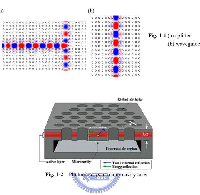
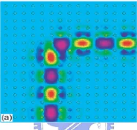
During the past decade the use of photonic crystals (PhCs) has been studied and risen from an indistinct technology to a prominent field of research [1,2]. This is mainly because of their potential ability to well control the propagation of light. Eli Yablonovitch [3] and Sajeev John [4] initially predicted the idea that a periodic structure consisting of materials with different dielectric constants possesses bandgaps for certain ranges of the frequency, in much the same way as an electronic bandgap exists in semiconductor materials. Photonic crystal with defects can be found much more applications. Defects in photonic crystals means the points or places different from perfectly arrayed structures. Defects just like missing a point, line or dislocations can create defect modes within the photonic band gap. Using this property, photonic crystals can modify the spontaneous emission efficiency and the propagation of light, leading to novel applications in splitter, waveguides (Fig. 1-1), defect-mode light-emitters, electro-optical switch [5], Mach-Zehnder interferometer [6], and micro-cavity lasers (Fig. 1-2) [7–10], etc. This is why many scholars believe that the PhCs bring us a possible solution and unlimited vision of creating large-scale photonic integrated circuits (PICs) in the future and have done more and more studies on photonic crystals. Numbers of reports focusing on the design of PhC’s devices in PICs have been published in the last few years [11].
(a) (b)
Fig. 1-1 (a) splitter
(b) waveguide
Fig. 1-2 Photonic-crystal micro-cavity laser
Two-dimension photonic crystals are regarded as the hottest topic nowadays, because they offer the possibility of fabricating high-Q cavities [12-13] and waveguide devices [14] on the scale of the wavelength in the semiconductor-based structures (i.e. GaAs/AlGaAs or SOI). Photonic integrated circuits of similar integration density so far only known as electronic VLSI (Very Large Scale Integrated Circuits) can be imagined. Photonic crystal waveguide (PCW) is an important basic element in PICs [15, 16] as important as the electric wire in the electric circuits. It is the key component of interconnect between optical circuits. Optical waveguiding in two-dimension photonic crystals is achieved by introducing line defects in the structure that is otherwise periodic in two dimensions.
When we take photonic crystal as basic structure of waveguide, another important characteristic of photonic crystal is its unusual dispersion property. Group velocity
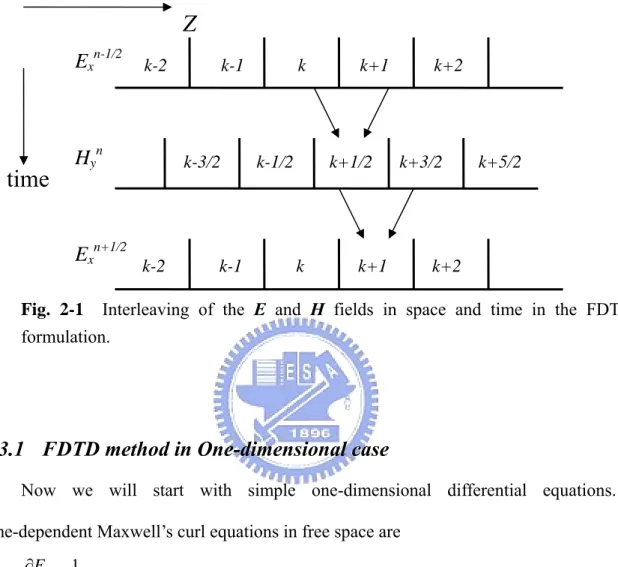
dispersion of line defect in photonic crystal slabs is experimentally proved to be extremely large, and can be tuned via adjusting the widths of defects [17]. In conventional total internal reflection (TIR) waveguide, the bending angle for changing light propagation direction cannot be over 1o, otherwise the loss will be quite big. Different from the conventional waveguides, photonic crystal band gap (PBG) and large group velocity of PCWs can still keep well guiding the signal even if they form sharp-bend, as shown in Fig. 1-3.
Fig. 1-3 Distribution of the real part of electric field in a 90o bend of
the dielectric rods PCs. The red color shows positive
amplitude of electric field and the blue for negative amplitude.
Two closely parallel waveguides can be used as a directional waveguide coupler [18-22]. A directional waveguide coupler is also one of key components for optical communication. They can be used as wavelength-selective power dividers, switches, modulators, etc. [23, 24] Besides, it might be desirable to decouple the two waveguides to minimize cross talk between them, for example, when envisioning closely packed photonic wires in integrated optical circuits [25].
Other phenomena of two-dimension PhCs had also been widely discussed, including coupling/decoupling, energy flow [26], and extremely low group velocity [27-28]. All of those researches make us getting closer and closer to entirely grasp this new technologies.
1-2 Motivation
In order to prepare for arrival of the next-generation optical communication, many scholars try to develop new optical devices which possess tiny scale, high efficiency, integrabilility and easy fabrication. Fortunately, people found some kinds of man-made materials called photonic crystals that make all our imagination realizable. By introducing different defects into perfect photonic crystals, many abilities such as wave-guiding, light-trapping, filtering, slowing light and light coupling could all be generated at will. With integrating such devices in a single chip, large photonic integrated circuits provide a wide view of future information technology. People even predict the coming of the photonic computer in the next ten years.
For optical communication systems used now, the size of the wavelength dependent power splitter is about hundreds of micrometer. If one can reduce the size of photonic crystal directional coupler devices to ten of micrometers, it should provide a great advantage for wavelength division multiplexing (WDM) systems. This provides the motivation to develop an effective numerical method for analyzing coupling between channel waveguides in a two-dimension photonic crystal. In the previous research, a photonic crystal waveguide is formed by a chain of point defects, so the waveguide can be regarded as a coupled-cavity waveguide (CCW), in which the energy can hop from a cavity to the neighbor one. The propagation of wave through a CCW is exactly the classical wave analog of the tight-binding (TB) method in solid state physics. It also indicates that there exists a large potential in designing various compact photonic devices by using the large dispersion of coupled mode splitting. According to this idea, we can do the design of PhC devices applying in optical communication with micrometer scale. In the following chapter, we will present two topics focusing on physical insight in PhC waveguides with tight-binding theory and optical devices
such as WDM based on photonic crystal with silicon rod array. In order to design WDM, we need to know the coupling length at each frequency. According to the coupling length formula L=π/Δk, we must know the value of Δk in order to calculate the coupling length. Although we can obtain a band structure through the plane wave expansion (PWE) method, it needs to extensive calculation to generate good resolution of dispersion curve, especially for the decoupling point of two identical photonic crystal waveguides (PCWs). By using the dispersion function derived from the tight-binding theory, we can well fit the calculated dispersion curves of the derived dispersion function. In turn, we can easily calculate the coupling length at corresponding frequency using the dispersion relation function. Therefore, few data of dispersion relation calculated from the PWE are enough to determine the dispersion function and the decoupling point.
1-3 Organization of the thesis
We divided this thesis into four chapters. We have narrated a brief statement to the background and history of the photonic crystal and also our research motivations in chapter 1. The main theory and numerical analysis methods we depended will put in chapter 2. After that, in the chapter 3 we will describe our approaches to the coupling problem between PCWs and our PhC optical device design and the simulation results. In the end, the final conclusion will be presented in chapter 4.
Chapter 2 Calculation Method and Theory
As same as all studies of the electromagnetism, analyses to the propagation of light in a photonic crystal also start with four macroscopic Maxwell’s equations. In cgs units, they are
πρ 4 0 = ⋅ ∇ = ⋅ ∇ D B , 4 1 0 1 J c t D c H t B c E π = ∂ ∂ − × ∇ = ∂ ∂ + × ∇ (2.1)
where E and H are the macroscopic electric and magnetic fields, D and B are the electric displacement and magnetic induction fields, and ρ and J are free charge and current densities, respectively. Here we are concerned with the behavior of an electromagnetic wave in a source-free region where free charge ρ and free current J in Eq. (2.1) are both zero.
2-1 Introduction
In order to solve the wave equations derived from Maxwell’s equations, we need the constitution equations relating D to E and B to H. Since we do not deal with magnetic material, we assume the magnetic permeability µ is very close to unity and we may set
. ) , ( ) , (r t H r t Bv v = v v
As for D and E, quite generally the components Di of the displacement field are related
to the electric field components Ei by the following power series [1]:
.) ( 3
∑
+∑
+Ο = j j k j ijk j ij i E k E E E D ε χ (2.2)To simplify the question, we make four assumptions. First we usually assume the field strengths are small enough so that we are in the linear regime. It means χ and all higher order terms can be ignored. Second, we assume the material is macroscopic and isotropic, so that E(r,ω) and D(r,ω) are related by a scalar dielectric constant ε(r,ω). Third, any explicit frequency dependence of the dielectric constant are also been ignored. The last
assumption is that we focus only on low-loss dielectrics, which means ε(r) is treated as pure real. Hence, we have a brief expression relating D and E fields as
). ( ) ( ) (r r E r D =ε (2.3)
With four assumptions above, the Maxwell’s equations [Eq. (2.1)] become
0 ) , ( ) ( 0 ) , ( = ⋅ ∇ = ⋅ ∇ t r E r t r H ε . 0 ) , ( ) ( ) , ( 0 ) , ( 1 ) , ( = ∂ ∂ − × ∇ = ∂ ∂ + × ∇ t t r E c r t r H t t r H c t r E ε (2.4)
The field functions E and H generally are both complicated functions of time and space, but thanks to the linearity of Maxwell's equation, it is convenient to look for solutions in form of harmonic fields: t i t i e r E t r E e r H t r H ω ω ) ( ) , ( ) ( ) , ( = = . (2.5)
Because there is no free charge and current, the electromagnetic waves considered to be transverse. By substituting Eq. (2.5) into Eq. (2.4) we can obtain the following equations:
) ( )} ( { ) ( 1 ) ( 2 2 r E c r E r r E E v v v v v v v ω ε ∇× ∇× = ≡ Θ (2.6) ) ( )} ( ) ( 1 { ) ( 2 2 r H c r H r r H H v v v v v v v ω ε ∇× = × ∇ ≡ Θ . (2.7)
Solving Eqs. (2.6) and (2.7) is to solve the eigen-value problems, and is a Hermitian operator. The eigenvectors H(r) and
H Θ ) ( ~ r
E (whereE~(r)= ε(r)E(r)) are the field patterns
of the harmonic modes, and the eigenvalues ( )2
c ω
are proportional to the square frequencies of those modes.
The Maxwell’s equations are the most important kernel of following calculations (both PWE and FDTD) and analyses in the next chapter except only the tight-binding approximation by solid-state physics that we’ll discuss later.
2-2 Plane-wave expansion method
Photonic crystals is a periodically arranged structure (i.e., its dielectric constant is periodic distributed), so we assume that the dielectric constant is real, isotropic, perfectly periodic with the spatial coordinate rv , and does not depend on frequency. Hence we can write its dielectric function as
( )r (r i)
ε v =ε v+ av , i=1,2,3, (2.8) where are the primitive lattice vectors of the photonic crystal. Because of the spatial
periodicity, we introduce the primitive reciprocal lattice vectors {b { }avi
i ; i=1,2,3} and the reciprocal lattice vector can be defined as {G}:
2
i⋅ j = πδij
a b
and G=l1 1b +l2 2b +l3 3b , (2.9) where { } are arbitrary integers and li δ is the Kronecker’s delta function. We can expand ij
into Fourier series as ) ( 1 rv − ε
∑
⋅ = G r iG G r) ( )exp( ) ( 1 κ ε . (2.10)Because ε is a periodic function of the spatial coordinate r, we can apply Bloch’s theorem to Eqs. (2.6) and (2.7). and are thus characterized by a wave vector k in the first Brillouin zone and a band index n and expressed as
) (r E H(r) r ik kn kn r u r e E r E( )= ( )= ( ) ⋅ (2.11) r ik kn kn r v r e H r H( )= ( )= ( ) ⋅ , (2.12) where and ukn(r) vkn(r) are periodic vectorial functions:
) ( ) (r a u r ukn + i = kn (2.13) ) ( ) (r a v r vkn + i = kn , for i=1,2,3. (2.14)
These periodic functions can be expanded in Fourier series as 1( ) in Eq. (2.10). The r
−
two Fourier expansions of the fields can be derived as the following form of the eigenfunctions: } ) ( exp{ ) ( ) (r E G i k G r E G kn kn =
∑
+ ⋅ (2.15) } ) ( exp{ ) ( ) (r H G ik G r H G kn kn =∑
+ ⋅ . (2.16)The expansion coefficients in reciprocal lattice space, i.e., and are denoted by the same symbols as the original ones in real space. Substituting Eq. (2.15), (2.16), (2.11) and (2.12) into (2.6) and (2.7), we obtain the following eigenvalue equations for the expansion coefficients { } and { }:
( ) kn E G Hkn( )G ( ) kn E G Hkn( )G ) ( )} ' ( ) ' ( ) ' ){( ' ( 2 2 ' G E c G E G k G k G G kn kn kn G ω κ − + × + × = −
∑
(2.19) ) ( )} ' ( ) ' {( ) )( ' ( 2 2 ' G H c G H G k G k G G kn kn kn G ω κ − + × + × = −∑
, (2.20)where ωkn denotes the eigen-angular frequency of and . The vector
electromagnetic field in the 2D photonic lattice can be decomposed into two independent polarization components, i.e., an E polarization (TM mode) for which the electric field is parallel to the rod axis (E
) (r
Ekn Hkn(r)
z only), and an H polarization (TE mode) for which the magnetic
field is parallel to the rod axis (Hz only). In two-dimensional photonic crystals, Eq. (2.19)
and Eq. (2.20) reduce to 2 1 2 ' | ' || | ( ') ( ')} kn ( kn kn G k G k G G G E G E G c ω ε− + + − =
∑
) , (2.21)where Eq. (2.21) is the master equation of TM mode. Similarly, the master equation of TE mode can be written as
2 1 2 ' ( ') ( ) ( ') ( ')} kn ( kn kn G k G k G G G H G H G c ω ε− + + − =
∑
) . (2.22)For the photonic band calculating, the expansion coefficients { } in Eq. (2.10) is necessary to be calculated by the plane-wave expansion method. The inverse Fourier transform gives 1( ) G ε− 1( ) 1 1( ) exp( ) V G dr r iG V ε− = ε−
∫
− r , (2.23)where V is the volume of the unit cell of the photonic crystal. In general, this integral should be numerically evaluated by FFT method. However, if the shapes of the dielectric components in the unit cell are simple enough, we can calculate it analytically.
2-3 Finite-difference time domain method (FDTD) [29]
The finite-difference time-domain method is introduced by Yee in 1966 [30]. During the 1970s and 1980s, several defense agencies working in the areas motivated large-scale solutions of Maxwell’s equations. The entire field of computation electrodynamics is shifting rapidly in high-speed communications and computing. In 1990, engineers in the general electromagnetic community became aware of the modeling capabilities afforded by FDTD and related techniques, and the interest in this area has expanded well beyond defense technology. The main reason to introduce FDTD method to solve photonic crystal is that when the structure is too complex, it is hard to solve Maxwell’s equation in frequency domain. FDTD provide a straight forward way to solve it in time domain. With this method, we can see the field distribution in photonic crystals. In addition, there are several advantages in FDTD method. First, FDTD is accurate and robust. The sources of error are well known. Second, being a time domain technology, FDTD treats impulsive behavior and nonlinear behavior naturally. Third, FDTD uses no linear algebra. Being a fully explicit computation, FDTD avoids the difficulties with linear algebra that limit the size of frequency-domain integral-equation.
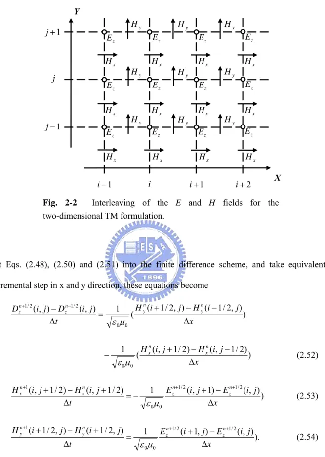
When the differential forms of Maxwell's equations are examined, it can be seen that the time derivative of the E field is related to the curl of the H field ( ). This can be simplified to state that the rate of the change in the E field (the time derivative) depends on the change in the H field across space (the curl). The results in the basic FDTD equations are that the new value of the E field is related to the old value of the E field (hence the
H × ∇
difference in time) and the difference of old values of the H fields on either side of the E field point in space. Naturally, this is a simplified description as illustrated in Fig. 2-1.
Z
E
xn-1/2 k-2 k-1 k k+1 k+2H
y n k-3/2 k-1/2 k+1/2 k+3/2 k+5/2time
E
x n+1/2 k-2 k-1 k k+1 k+2Fig. 2-1 Interleaving of the E and H fields in space and time in the FDTD
formulation.
2-3.1 FDTD method in One-dimensional case
Now we will start with simple one-dimensional differential equations. The time-dependent Maxwell’s curl equations in free space are
H t E = ∇× ∂ ∂ 0 1 ε (2.24) . 1 0 E t H =− ∇× ∂ ∂ µ (2.25)
Here E and H are vectors in three dimensions. When we consider only in one dimension
case, E and H simply have Ex and Hy components, so Eq. (2.24) and (2.25) become
z H r t Ex y ∂ ∂ − = ∂ ∂ 0 ) ( 1 ε ε (2.26) . 1 0 z E t Hy x ∂ ∂ − = ∂ ∂ µ (2.27) Above equations mean the electric field oriented in the x direction and the magnetic field
oriented in the y direction both traveling in the z direction. Taking the central difference approximation for both the temporal and spatial derivatives gives
z k H k H r t k E k E ny n y n x n x ∆ − − + − = ∆ − − + ( 1/2) ( 1/2) ) ( 1 ) ( ) ( 0 2 / 1 2 / 1 ε ε (2.28) . ) ( ) 1 ( 1 ) 2 / 1 ( ) 2 / 1 ( 1/2 1/2 0 1 z k E k E t k H k H n x n x n y n y ∆ − + − = ∆ + − + + + + µ (2.29)
In these two equations, “n” actually means a time t=∆t⋅n. The term “n+1” means one time step later; “k” actually means the distance z=∆z⋅k. The formula of Eqs. (2.28) and (2.29) assume that E and H fields are interleaved in both space and time. H uses the arguments and to indicate that the H field values are assumed to be located between the E field values. Similarly, superscript
2 / 1 + k k−1/2 2 / 1 + n or indicates
that it occurs slightly after or before n, respectively. Eq. (2.28) and (2.29) can be rearranged as 2 / 1 − n )] 2 / 1 ( ) 2 / 1 ( [ ) ( ) ( ) ( 0 2 / 1 2 / 1 + − − ∆ ⋅ ∆ − = − + k H k H z r t k E k Exn xn yn yn ε ε (2.30) )]. ( ) 1 ( [ ) 2 / 1 ( ) 2 / 1 ( 1/2 1/2 0 1 k E k E z t k H k H xn n x n y n y + + + + − ∆ ⋅ ∆ − + = + µ (2.31)
The calculations are interleaved in both space and time. This is the fundamental paradigm of the finite-difference time-domain (FDTD) method. Eqs. (2.30) and (2.31) are very similar, but because ε0 and µ0 differ by several orders of magnitude. This is circumvented by making the following change of variables:
. ~ 0 0 E E µ ε = (2.32)
Substituting (2.32) into (2.30) and (2.31) gives
)] 2 / 1 ( ) 2 / 1 ( [ 1 ) ( ~ ) ( ~ 0 0 2 / 1 2 / 1 + − − ∆ ∆ − = − + k H k H z t k E k Exn xn yn yn µ ε ε (2.33) )]. ( ~ ) 1 ( ~ [ 1 ) 2 / 1 ( ) 2 / 1 ( 1/2 1/2 0 0 1 k E k E z t k H k Hny+ yn xn+ + − xn+ ∆ ∆ − + = + µ ε (2.34)
If the cell size ∆z is chosen, the time step ∆ can be determined by t 0 2 z t c ∆ ∆ ≥ ⋅ (2.35) where c0 is the light speed in free space. The reason why we determined the time step t∆
to Eq. (2.30) related to the stability of the FDTD method. An electromagnetic wave propagating in free space cannot go faster than the speed of light. To propagate a distance of one cell ∆z needs a minimum time of
0
c z t = ∆
∆ . When we get to two-dimensional
simulation, we have to allow for the propagation in the diagonal direction, which brings the time requirement to
0
2c z t= ∆
∆ . Obviously, three-dimensional simulation requires
0
3c z t = ∆
∆ . This is summarized by the well-known “Courant Condition” [31, 32]:
, 0 c d z t ⋅ ∆ ≤ ∆ (2.36)
where d is the dimension of the simulation. Hence we will determine in Eq. (2.37). This is not necessarily the best formula! Therefore,
t ∆ 2 1 2 / 1 0 0 0 0 = ∆ ⋅ ∆ ⋅ = ∆ ∆ z c z c z t µ ε (2.37)
Substituting (2.35) into (2.33) and (2.34), those equations become
1/ 2( ) 1/ 2( ) 0.5( ( 1/ 2) ( 1/ 2)) n n n n x x y y E k E k H k H k ε + = − − + − − % % (2.38) 1( 1/ 2) ( 1/ 2) 0.5[ 1/ 2( 1) ( )] n n n n y y x x H + k+ =H k+ − E% + k+ −E% +1/ 2 k (2.39) Besides the last two iterative equations, we still need to add incident wave source condition and absorbing boundary condition. It is a great subject in dealing with the wave source condition. For simplicity, we divide it into two categories in 1-D case: hard source and soft source. In a hard source, a propagation wave will see that value and be reflected, because the hard value of Ex looks like a metal wall to FDTD. However a soft source is added to Ex at a certain point and a propagating pulse will just pass through. In calculating
photonic crystal, we must consider the field scattering from the material. Therefore we use a soft source.
sin(2
* * )
x xpulse
f
dt t
E
E
pulse
π
=
=
+
(2.40)In order to keep outgoing E and H fields from being reflected by the calculation boundary and back into the problem space, so the absorbing boundary conditions (ABC) are necessary to consider. The fields at the edge must be propagating outward. In one time step of the FDTD algorithm it travels
distance = 2 2 0 0 0 x c x c t c = ∆ ⋅ ∆ ⋅ = ∆ ⋅ . (2.41)
This equation basically explains that it takes two time steps for a wave front to cross one cell. So a common sense approach tells us that an ABC might be
2 2 (0) (1) ( ) ( 1), n n x x n n x x E E E k E k − − = = − (2.42)
where 0 and k are the end points and n is a time step. Simply store a value of Ex(1) two time
steps before in Ex(0). Boundary conditions such as these have been implemented at both
ends of the Ex array. Below are the examples of C computer code in one-dimensional
absorbing boundary conditions. Additional parameters are used to store the boundary value for two time steps during the calculation loop.
ex[0] = ex_low_m2; ex_low_m2 = ex_low_m1; ex_low_m1 = ex[1]; (243) ex[KE-1] = ex_high_m2; ex_high_m2 = ex_high_m1; ex_high_m1 = ex[KE-2];
2-3.2 Two-dimensional photonic crystal formulation and perfectly matched
layer (PML) boundary condition
We start again with the normalized Maxwell’s equations:
H t D × ∇ = ∂ ∂ 0 0 1 ~ µ ε (2.45) ) ( ~ ) ( ) ( ~ ω ε ω ω E D = r ⋅ (2.46) . ~ 1 0 0 E t H × ∇ − = ∂ ∂ µ ε (2.47) where E Ev 0 0 ~ µ ε = and D Dv 0 0 1 ~ µ ε
= . In two dimension cases, there exist two groups of
six different fields. One is the transverse magnetic (TM) mode, which is composed of E~z, , and . Another is the transverse electric (TE) mode, which is composed of ,
x
H Hy E~x E~y,
andHz. In TM mode, therefore, Eq. (2.44) ~ (2.47) are reduced to
) ( 1 0 0 y H x H t Dz y x ∂ ∂ − ∂ ∂ = ∂ ∂ µ ε (2.48) ) ( ) ( ) (ω εr ω z ω z E D = ⋅ (2.49) y E t Hx z ∂ ∂ − = ∂ ∂ 0 0 1 µ ε (2.50) . 1 0 0 x E t H z y ∂ ∂ = ∂ ∂ µ ε (2.51)
The two-dimensional systemic interleaving of the calculated fields is more complex than one dimension. That is illustrated in Fig. 2-2 below.
Y
y
H
y
H
Put Eqs. (2.48), (2.50) and (2.51) into the finite difference scheme, and take equivalent incremental step in x and y direction, these equations become
) ) , 2 / 1 ( ) , 2 / 1 ( ( 1 ) , ( ) , ( 0 0 2 / 1 2 / 1 x j i H j i H t j i D j i D ny n y n z n z ∆ − − + = ∆ − − + µ ε ) ) 2 / 1 , ( ) 2 / 1 , ( ( 1 0 0 x j i H j i Hnx xn ∆ − − + − µ ε (2.52) ) ) , ( ) 1 , ( 1 ) 2 / 1 , ( ) 2 / 1 , ( 1/2 1/2 0 0 1 x j i E j i E t j i H j i Hxn xn zn zn ∆ − + − = ∆ + − + + + + µ ε (2.53) ). ) , ( ) , 1 ( 1 ) , 2 / 1 ( ) , 2 / 1 ( 1/2 1/2 0 0 1 x j i E j i E t j i H j i H n z n z n y n y ∆ − + = ∆ + − + + + + µ ε (2.54)
We have briefly mentioned the issue of absorbing boundary conditions (ABCs) in discussion of one dimension. In the two-dimensional simulations, the program contains two-dimensional matrices for the values of all the fields (i.e. dz, ez, hx and hy). Assume we
X 1 + j j 1 − j 1 + i i+2 1 − i i x H z E z E z E z E z E z E z E z E z E z E z E z E y H x H Hx H x y H y H Hy x H Hx Hx H x y H Hy Hy x H Hx Hx H x
Fig. 2-2 Interleaving of the E and H fields for the
are simulating a wave generated from a point source propagating in the free space. As the wave propagates outward, it will eventually come to the edge of the allowable space, which is dictated by how the matrices have been dimensioned in the program. If we had done nothing about this, reflections would be produced and would go back the problem space. Then we will have no way to differentiate between the real wave and the reflected wave. This is why the ABCs must exist. The most effective ABCs is the perfectly matched layer (PML) developed by Berenger [32]. How PML works can be easily understood by the following description. If a wave propagating in medium A and it impinges upon medium B, the amount of reflection can be determined by the intrinsic impedances of two media
B A B A η η η η + − = Γ , (2.55)
where the impedance is . ε µ
η = If µ changed with ε so η still remained a constant, Γ would
be zero and no reflection will occur. But this is still helpless to our problem, because waves will continue propagating in the new medium. We really want is a medium that is also lossy so the wave will decrease before it hits the boundary. Hence we mark both ε and µ of complex due to their imaginary parts causing decay.
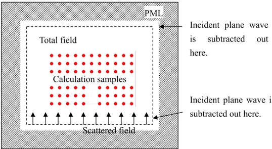
To simulate a plane wave propagating in a 2D FDTD program, the space of problem will be divided into two regions, the total field and the scattered field (Fig. 2-3). There are two reasons for doing this: (1) The propagating plane wave should not interact with the absorbing boundary conditions; (2) the load on the absorbing boundary conditions should be minimized. These boundary conditions are not perfect. By subtracting the incident field, the amount of the radiating field hitting the boundary is minimized, thereby reducing the calculation error.
PML
Incident plane wave is subtracted out here.
Total field
Calculation samples
Incident plane wave is subtracted out here. Scattered field
Fig. 2-3 Total field/scattered field of the two-dimensional problem space.
2-4 Tight binding method in solid state physics
In the later discussion of the coupling between the photonic crystal waveguides we will apply the tight binding approximation to support our argument. So we here do a simple introduction of what is the tight binding method and its meaning in solid state physics [33].
In atoms the electrons are tightly bound to their nuclei. If the atoms are so close that their separations become comparable to the lattice constant in solids, their wave functions will overlap each other. If we consider only two atoms, their combined wave functions are
B
A ψ
ψ ± . The electron energy of state ψA+ψB is lower than one of state ψA−ψB. After they approach to each other, the Coulomb force between nucleuses and electrons can cause the energy level splitting and becomes energy band. The approximation method to obtain the energy band structure by calculating the free atomic wave functions is called tight binding approximation (TB) or linear combination of atomic orbitals (LCAO). In covalently bonded semiconductors the valence electrons are concentrated mainly in the bonds. Therefore the wave functions of valence electrons should be very similar to bonding orbitals
found in molecules. In addition to being a good approximation for calculating the valence bond structure, the TB method has the advantage that the band structure can be defined in terms of a small number of overlap parameters. The overlap parameters have a simple physical interpretation as representing interactions between electrons of adjacent atoms.
Assume that an electron with ground state ϕ(r) exercises within a single atom’s potential U(r), where ϕ(r) denotes as the s state. It is too complex if we solve the energy band problem by using degenerated atomic energy levels. Therefore, we assume that the influence between two atoms is quite small, and then the wave function can be expanded as following:
∑
− = j j kj k(r) C ϕ(r r ) ψ . (2.56)If in Eq. (2.56) is for a crystal with N atoms, the Bloch form of the above equation can be expressed as
j r ik j k N e C , = −1/2 ⋅
∑
⋅ − = − j j k(r) N exp(ik r) (r r ) 2 / 1 ϕ ψ , )ψk(r+T)=exp(ik⋅T)ψk(r , (2.57)where T is the primitive vector connecting two lattice points. To calculate the 1st level energy by doing the Hamiltonian matrix diagonalization as follow:
, )] ( exp[ 1 j m j m m j r H r ik N k H k = −
∑∑
⋅ − ϕ ϕ (2.58) where )ϕm ≡ϕ(r−rm . Let ρm =rm −rj, then∑
⋅∫
− = m m m dV r H r ik k H k exp( ρ ) ϕ*( ρ ) ϕ( ). (2.59)In Eq. (2.59), we do the integration to only an atom and other atoms nearby which are tied up by ρ . We can rewrite it as:
∫
dVϕ*(r)Hϕ(r)= a− ;∫
dVϕ*(r−ρ)Hϕ(r)=−γ (2.60) To set k k =1, the 1st level energy is∑
⋅ = − − = m k m ik a k H k γ exp( ρ ) ε . (2.61)The relation between overlapping energy γ and atomic spacing ρ in two hydrogen atoms which are both in the 1s state can be clearly calculated. Using the Rydberg-energy unit,
, we have 2 4 / h2 me Ry= ) / exp( ) / 1 ( 2 ) (Ry ρ a0 ρ a0 γ = + − . (2.62) Considering to a simple cubic structure, the positions of the closest atoms are
); 0 , 0 , ( a m = ± ρ (0,±a,0); (0,0,±a). (2.63) So Eq. (2.61) becomes ) cos (cos 2 k a k a k a a x y z k =− − γ + + ε . (2.64)
Other example likes the fcc structure which has twelve closest atoms and its band structure can be described as ) 2 1 cos 2 1 cos 2 1 cos 2 1 cos 2 1 cos 2 1 (cos 4 k a k a k a k a k a k a a y z z x x y k =− − γ + + ε . (2.65)
Hence the tight-binding approximation method provides a very simple way to do the atomic energy band structure analysis. This way can also be applied to discussion of the small coupling effect inside a photonic crystal coupled-cavities waveguides (CCWs).
Chapter 3 Simulation and Discussion
In this chapter, we will bring up a series of research focusing on both waveguide properties and 2-D photonic crystals devices. Two subjects have been discussed in the following text, including tight-binding theory of coupling behavior in the PhC waveguides and WDM design using resonant ring devices. Many related and additional points have also been analyzed.
3-1. Long-range interaction of defect modes between coupled
identical photonic crystal waveguides
When two identical photonic crystal waveguides (PCWs) are placed close to each other, a “band-crossing” property could be found in the dispersion relation. We use MIT photonic band code to investigate the band structures with void and reduced line-defects in square and triangular lattices and coupling between two PCWs in silicon rod array. By using the tight-binding (TB) approximation, we fit the dispersion curves very well and accurately define the crossing point of dispersion curves.
3-1.1
Single line defect photonic crystal waveguides and
tight-binding approximation
The PCW couplers consist of plural adjacent PCWs in which the guided modes are overlapped, resulting the splitting of dispersion curves. That is in common with its counterpart built with conventional optical waveguides. However, there is certain fundamental dissimilarity between these two categories of couplers. One remarkable example is the decoupling of the adjacent waveguides. Decoupling occurs where the dispersion curves of the split guided modes cross, namely the degeneracy has not be
removed at a certain frequency. To generate decoupling is an exhausting task to conventional waveguides, but a direct effect for PCWs [35-37].
Typically, the dispersion curves of the PCW couplers can be obtained numerically from the solutions of Maxwell’s equations by the plane wave expansion (PWE) method [38]. However, the PWE does not provide enough insights to the coupling mechanism of PCWs. Also, there are very few literatures discussing this mechanism. In this thesis, we explain the PCW coupling with the long-range interactions among the eigenmodes of individual defects and derive the evolution equation of the guided modes. The split of the dispersion curves is attributed to the cross-waveguide coupling to the nearest neighboring (NN) defects and the next NN defects in the second PCW. The dispersion curves cross due to the cancellation of these two couplings, causing the decoupling of the PCWs.
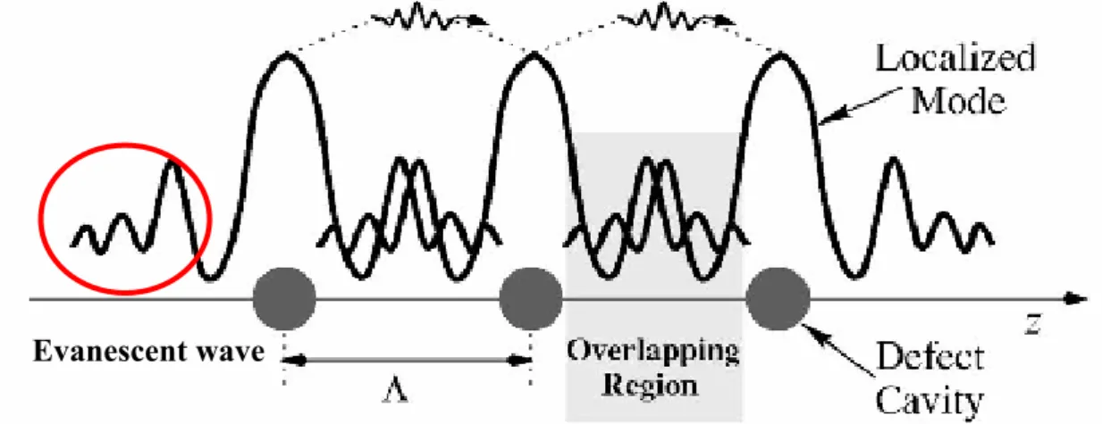
A point defect, acts as an optical resonator (cavity), can be created by introducing a single defect into a photonic crystal that locally trap photons with a certain frequency inside the defect volume (Fig. 3-1(a)). The coupled cavity waveguide (also referred to as coupled resonator optical waveguide) composed of well-separated defects in PhC (Fig. 3-1(b)) has been proposed and demonstrated recently [39, 40]. It is assumed the defects are weakly coupled due to the overlapping of the individual evanescent eigenmodes (here referred to as defect modes) and the dispersion relation can be obtained by the formalism developed from the tight-binding (TB) approximation in solid state physics (Fig. 3-2). Only the couplings with the nearest neighboring (NN) defects are taken into account in this approximation as the defect modes are localized in the defect sites. The defects beyond the NN ones are ignored.
Conceivably, a PCW can be regarded as a chain of consecutive defects, and the dispersion relations of the guided modes result from the superposition of longitudinal shifted defect modes. The coupling concept of the TB approximation is borrowed to model the dispersion relation in PCWs. Notably, the consecutive defects are still too close and the coupling beyond the NN defects is significant, which cannot be ignored in the evolution equation [41]. As the couplings to the remote defects are taken into account, the evolution equation extended from the TB approximation can be written as
Fig. 3-1 (a) A single point defect, in which the photon in resonance
frequency is trapped inside the point defect. (b) A diagram of coupled cavity waveguide (CCW).
Evanescent wave
Fig. 3-2 Schematics of propagation of photons by the coupled
∑
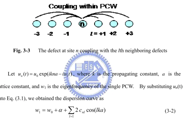
= + − + + + = ∂ ∂ 1 0 ) ( ) ( l l n l n nl n n w u c u u u t i α (3-1)un represents the Bloch function at site n, w0 is the resonant frequency of a single
cavity, α is a small shift (arising from the presence of neighboring defect) in the eigenfrequency of the single point defect and cnl is the coupling coefficient of the
defect at site n with the l-th neighboring defects as illustrated in Fig. 3-3.
Fig. 3-3 The defect at site n coupling with the lth neighboring defects
Let , where k is the propagating constant, is the lattice constant, and w
) exp(
)
(t u0 ikna iw1t
un = − a
1 is the eigenfrequency of the single PCW. By substituting un(t)
into Eq. (3.1), we obtained the dispersion curve as
∑
= + + = 1 0 1 2 cos( ) l nl lka c w wα
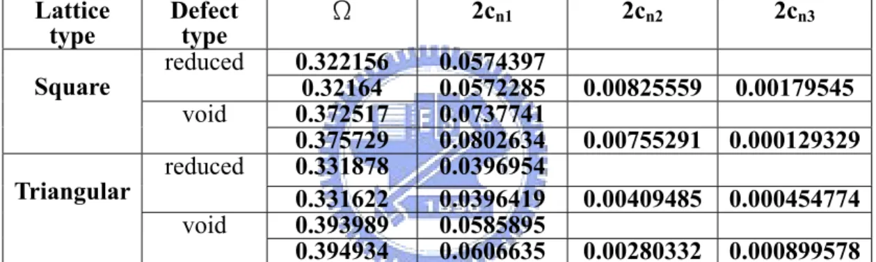
(3-2) The formula is applied to fit the dispersion curve of a single PCW derived from PWE. Two-dimensional (2D) PhCs consisting of a triangular lattice and a square lattice of dielectric rods with the lattice constant in air were considered. Assume the PCW is formed by a line defect of void (Ra
d=0a) and reduced rods (Rd=0.1a) in a two dimensional PhC of both array of circular rods. Let the dielectric constant of the rod is 12 and the radius of the rod is 0.2 . The dispersion curves derived from PWE (the dotted curve in Fig. 3-4) is fitted with Eq. (3-2) (the dash curve) as only the couplings with NN defects (l = 1) are involved. Obviously, the NN couplings are insufficient to accurately determine the dispersion curve, and the mode functions in a
PCW appear not well-localized. The curve is well fitted as long as the long-range couplings up to the third NN defects are taken into account, presented as the solid curve in Fig. 3-5. Therefore, Eq. (2) is recast as
)
3
cos(
2
)
2
cos(
2
)
cos(
2
1 2 3 1c
ka
c
ka
c
ka
w
=
Ω
+
n+
n+
n , (3-3)where is the sum of and α. , , and are the TB parameters determined from splitting of several coupled cavities or the width of defect band. Equation (3.3) states the different strength of each evanescent waves coupling to the neighbors. Each fitting parameters in different orders are shown in Table 3-1 below.
Ω w0 cn1 cn2 cn3
Table 3-1 Fitting curve function of a single PCW Lattice
type Defect type Ω 2cn1 2cn2 2cn3
0.322156 0.0574397 reduced 0.32164 0.0572285 0.00825559 0.00179545 0.372517 0.0737741 Square void 0.375729 0.0802634 0.00755291 0.000129329 0.331878 0.0396954 reduced 0.331622 0.0396419 0.00409485 0.000454774 0.393989 0.0585895 Triangular void 0.394934 0.0606635 0.00280332 0.000899578
Fig. 3-4 (a) (b) The dispersion of the reduce and remove line-defect mode in square
lattice and the fitting curve with NN approximation. (c) (d) The dispersion of the reduce and remove line-defect mode in triangular lattice and the fitting curve with NN approximation. 0 . 1 0 . 2 0 . 3 0 . 4 0 . 5 0 . 2 8 0 . 3 2 0 . 3 4 0 . 3 6 0 .
(a)
3 8 0 . 0 5 0 . 1 0 . 1 5 0 . 2 0 . 2 5 0 . 3 0 . 3 5 0 . 3 2 0 . 3 4 0 . 3 6 0 . 3 8 0 . 4 0 . 4 2(b)
(c)
0 . 1 0 . 2 0 . 3 0 . 4 0 . 5 0 . 3 2 0 . 3 4 0 . 3 6(d)
0 . 0 5 0 . 1 0 . 1 5 0 . 2 0 . 2 5 0 . 3 0 . 3 5 0 . 3 4 0 . 3 6 0 . 3 8 0 . 4 20 . 1 0 . 2 0 . 3 0 . 4 0 . 5 0 . 2 8 0 . 3 2 0 . 3 4 0 . 3 6 0 . 3 8
(a)
Fig. 3-5 (a) (b) The dispersion of the reduce and remove line-defect mode in square
lattice and the fitting curve with NNNN approximation. (c) (d) The dispersion of the reduce and remove line-defect mode in triangular lattice and the fitting curve with NNNN approximation. 0 . 0 5 0 . 1 0 . 1 5 0 . 2 0 . 2 5 0 . 3 0 . 3 5 0 . 3 2 0 . 3 4 0 . 3 6 0 . 3 8 0 . 4 0 . 4 2
(b)
0 . 1 0 . 2 0 . 3 0 . 4 0 . 5 0 . 3 2 0 . 3 4 0 . 3 6(c)
0 . 0 5 0 . 1 0 . 1 5 0 . 2 0 . 2 5 0 . 3 0 . 3 5 0 . 3 4 0 . 3 6 0 . 3 8 0 . 4 2(d)
3-1.2
Tight-Binding Theory of Coupling of Identical Photonic
Crystal Waveguides
The behavior of dispersion relation along the Γ-X direction in single waveguide has been introduced earlier before. Naturally, the coupling concept can be applied to all general case of defects in PhCs such as the coupled PCWs. We applied the long-range coupling to handle the interaction between two coupled identical PCWs when two waveguides are placed in close vicinity. Therefore, the couplings to the defects in the other PCW (referred to as the cross-PCW coupling) are included. We found the interaction is dominated by the cross-PCW coupling of defect at site n with NN defect (l = 0 defect) and the next nearest neighboring defects (l = +1 and -1 defects) in the other PCW as shown in Fig. 3-6. The evolution equations for two coupled parallel identical PCWs are expressed as
3 0 1 1 ( ) ( ) ( n n nl n l n l n n l i u w u c u u v v v t α = + − β + − ∂ = + + + + + + ∂
∑
γ n 1), (3-4) 3 0 1 1 ( ) ( ) ( n n nl n l n l n n l i v w v c v v u u u t α = + − β γ + n 1) ∂ = + + + + + + ∂∑
− , (3-5)respectively, where vn represents the Bloch function in the other PCW, and β and
γ separately represent the cross-PCW coupling coefficients with l = 0 and l = ±1 defects.
Let andun(t)=u0exp(ikna−iw2t) vn(t)=v0exp(ikna−iw2t) with w2 being the eigenfrequency of the coupled PCWs and substituted into Eqs. (3-4) and (3-5), then
Fig. 3-6 The defect at the nth site coupling with the lth defect in the other PCW.
the equations become 0 )] cos( 2 [ ) (w2 −w1 u0− β + γ ka v0 = , and (3-6) 0 )] cos( 2 [ ) (w2 −w1 v0 − β + γ ka u0 = (3-7) Therefore, the dispersion relations of the coupled PCWs can be obtained from the dependent Eqs. (3-6) and (3-7) as
)] cos( 2 [ 1 2 w ka w± = ± β + γ . (3-8) The dispersion curve of w1 is split into two curves denoted as and corresponding to an even and an odd supermode which will be mentioned later, due to the presence of cross-PCW coupling. Obviously, the coupling with l = 0 neighboring defect leads to a vertical shift by β merely, and couplings with l = 1 and -1 neighboring defects lead to the cosine modulation.
+ 2
w w2−
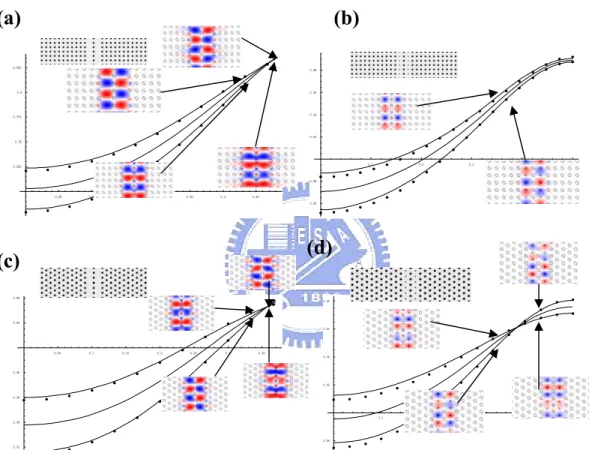
We applied Eq. (3-8) to fit the dispersion curves of the coupled PCWs derived from the PWE method. The coupled reduced-rod PCWs in a square lattices, shown in Fig. 3-7 (b) are treated. Since the coupling coefficients in w1 had been determined from fitting the dispersion curve of a single PCW with Eq. (3-3), the dispersion curves of + and were fitted by Eq. (3-8) with the known w
2
w w2− 1. The cross-PCW
coupling coefficients, β and γ, were obtained as 0.0094 and 0.00375. Evidently, the coupling of PCWs can be represented by cross-PCW couplings with l = 0 and ±1 defects in the second PCW. On the other hand, the curves of and in a triangular lattice can be fitted by the same approach as in Fig. 3-7 (d) to determine the coefficients, β and γ (0.0082 and 0.0054, respectively) as well. Here, we only include the cross-PCW coupling with l = 0 and ±1 defects, since they are dominant for the splitting of the dispersion curve. More cross-PCW coupling with farther defects should be included as more accurate determination of dispersion curves is demanded. It is noteworthy that the curves and in a triangular lattice
+ 2 w w2− + 2 w w2−
intersect, while it does not happen in the square lattice. Actually, all the three curves of w1, and intersect at one point in Fig. 3-7 (d). The triple intersection indicates that the split guided modes are degenerate and the PCWs are decoupled at the crossing point as if the adjacent PCW does not exist. All the fitting parameters of whole cases are shown in Table 3-2.
+ 2 w w2− 0.05 0.1 0.15 0.2 0.25 0.3 0.35 0.325 0.35 0.375 0.4 0.425 0.1 0.2 0.3 0.4 0.5 0.26 0.28 0.32 0.34 0.36 0.38
(a) (b)
0.05 0.1 0.15 0.2 0.25 0.3 0.35 0.32 0.34 0.36 0.38 0.42 0.44(d)
0.1 0.2 0.3 0.4 0.5 0.28 0.32 0.34 0.36 0.38(c)
Fig. 3-7 The energy band structures and their electric field patterns of the
defect modes of two coupled linear PCWs with both cases of remove and reduce rods in square lattice (a) (b) and triangular lattice (c) (d), which are split into two eigenmodes. The center lines are the defect of single PCW.
We conclude that the curves exhibit the competition between β and γ. The intersection occurs at k =[cos−1(−β/2γ)]/a, whereβ +2γ cos(ka)=0that means the effect of the couplings with l = 0 and ±1 defects are cancelled with each other. Accordingly, these three curves of w1, and are bound to intersect at one point. The inequality
+ 2
w w2− γ
β < 2 is a necessity for the intersection, it implies that the sum of
the coupling strength with the l = ±1 neighboring defects surpasses the coupling strength with the l = 0 defect. β (0.0094) > 2γ (0.0075) in the square lattice and
c
(a)
(b)
(d)
( )
Fig. 3-8 The energy band structures and their electric field patterns of the
defect modes of two coupled linear PCWs with both cases of remove and reduce rods in square lattice (a) (b) and triangular lattice (c) (d), which are split into two eigenmodes. The center lines are the defect of two PCWs.
β (0.0082) < 2γ (0.0108) in the triangular lattice support this argument.
Substituting Eq. (3-8) into Eqs. (3-6) and (3-7), we have the Bloch functions, u0 and v0, of w2+and w2− expressed as
⎟⎟ ⎠ ⎞ ⎜⎜ ⎝ ⎛ = ⎟⎟ ⎠ ⎞ ⎜⎜ ⎝ ⎛ + + 1 1 0 0 v u and ⎟⎟, ⎠ ⎞ ⎜⎜ ⎝ ⎛ − = ⎟⎟ ⎠ ⎞ ⎜⎜ ⎝ ⎛ − − 1 1 0 0 v u
respectively. It indicates the functions of appear to be even parity, while that of has the odd parity. The parities are in accordance with the results by the PWE method. In fact, which one of and is the lowest guided mode is determined by the sign of β. The β coefficients are positive in both of the square and triangular lattice cases. Therefore, the lowest guided mode is the odd-parity , opposite to the common understanding to conventional optical waveguides, in which the lowest mode is even. The lowest guided mode is even, if β is negative. The coupling coefficients represent the spatial integrations of the eigenfields involved. Hence, the spatial relationship of the eigenfield patterns can account for the parity of the lowest guided modes of the coupled PCWs.
+ 2 w − 2 w + 2 w w2− − 2 w
Table 3-2 Fitting curve function of two PCWs
Defect type β 2γ Mode
change Crossing point
Sq-reduce-1row 0.0093722 0.00747703 NO NO Sq-reduce-2row 0.00344394 0.00369485 NO NO Sq-remove-1row 0.00914204 0.0131291 Yes 0.373191 Sq-remove-2row 0.00369654 0.00321742 No No Tri-reduce-1row 0.00822751 0.0108092 Yes 0.383087 Tri-reduce-2row 0.00292783 0.0043047 Yes 0.366605 Tri-remove-1row 0.00905432 0.0155465 Yes 0.356311 Tri-remove-2row 0.00113095 0.00692431 Yes 0.287898
3-1.3 Summary
In summary, we have applied the concept of defect mode coupling to formulate the evolution equations of the coupled PCWs. The cross-PCW couplings to the 0th and ±1st neighboring defects in the other PCW account for the splitting of the dispersion curve of the coupled PCWs in both square and triangular lattices. The curves are modulated as a result of the competition between the couplings to the 0th and ±1st neighboring defects. Decoupling exists while those two couplings cancel each other. The parities of the Bloch functions also can be determined from the evolution equations.
3-2
Photonic crystal WDM design for application of coupling
Wavelength division multiplexing (WDM) plays an important role in optical communication. It allows network operators to more efficiently utilize bandwidth by aggregating separate wavelengths or channels onto a single optical fiber and offers an attractive solution to increasing the bandwidth of fiber network without disturbing the existing employed fiber trunk system. In order to develop the photonic integrated circuits (PICs) in the future, the device sizes are expected to be drastically reduced to a scale of a few tens of micrometers. Using photonic crystal devices may be a most possible solution to achieve integrated circuit. In this section, we will make a skeleton design of photonic crystal WDM using resonant rings. The simulation results are obtained using a finite difference time-domain method (FDTD) and a simpler coupled-mode theory.
3-2.1 Coupling of the directional coupler
We start with a device called photonic crystal directional coupler. When two PCWs are brought in close vicinity of each other they will form what is known as a directional coupler, shown in Fig. 3-9. Under proper conditions, the electromagnetic waves launched into one of the PCW can completely couple to the nearby waveguide. Under a precise calculation, two light waves can be split resulting from their own coupling length. According to this, a PhC WDM might be possibly fabricated. Although directional coupler has good transmission, unfortunately, based on the severe standard of extinction ratio in optical communication (20 dB is required in normal application), by using a usual directional coupler is pretty hard to achieve that performance. Figure 3-10 helps to catch on to this argument. In addition, directional coupler having large channel spacing is also a difficult to form WDM with more channels, even DWDM.