實驗及理論探討奈米結構之氧化鋅光學性質研究
177
0
0
全文
(2) 實驗及理論探討奈米結構之氧化鋅光學性 質研究 Experimental and theoretical study on the influence of finite crystallize optical properties in ZnO nanostructures 研 究 生:林 國 峰. Student:Kuo-Feng Lin. 指導教授:謝 文 峰 教 授. Advisor:Dr. Wen-Feng Hsieh. 國 立 交 通 大 學 光 電 工 程 研 究 所 博 士 論 文 A Dissertation Submitted to Department of Photonics and Institute of Electro-Optical Engineering College of Electrical Engineering and Computer Science National Chiao Tung University In Partial Fulfillment of the Requirements for the Degree of Doctor of Philosophy in Electro-Optical Engineering October 2008 Hsinchu, Taiwan, Republic of China 中華民國九十七年十月.
(3)
(4)
(5) 誌謝. 時間的流逝真是快速,轉眼間我即將離開這個具有充滿回憶的地方。回想 過去這幾年,在我腦海裡不斷的浮現出我所經歷的人事物,感覺到所有一切的事 都才剛剛發生而已,沒想到我即將要畢業了要進入我人生的另ㄧ段旅程了。 學習的過程是痛苦的,但是學習結果是甜美的。在這幾年裡,我特別要感謝 的指導老師謝文峰教授在我課業、實驗以及待人處世上的指導及教誨,以及實驗 室的學長們的指導使得我在學習過程中可以輕鬆自在。在我印象中,老師對教導 學生相當的具有有耐心,並且訓練學生養成具有邏輯思考的處事能力。在我的感 覺上老師就像是一位大家的好老爹!!!(雖然我曾被老爹定在黑板上近 2h 左右) 他總是跟我們這群調皮的學生聊一些天南地北的事情。另外,我要感謝口試委員 們對於論文上的指導及建議,使得論文更佳完整與周詳。在來要感謝雷射診斷實 驗室裡曾經陪伴我走過這幾年以來的夥伴們。政哥、信民學長當初在實驗上的指 導,也要感謝黃董、維仁、楊松精神及技術性上的指導。還有實驗室內可愛的學 弟妹們,使得我在這幾年內的生活多采多姿,真是太感謝你們了。還有那些曾經 跟我共存亡的同儕們,我們是共同經歷生死關卡的好同學、好朋友。在此我祝福 你們鵬程萬里、事事如意。 最後我要感謝我的父母親偉大的奉獻與支持,使得我在求學的路程中可以無 後顧之憂。還有感謝在我背後支持我的"那個人",謝謝你ㄧ直在我的背後這麼 的支持我!!!.
(6) 實驗及理論探討奈米結構之氧化鋅光學性質研究. 研究生: 林國峰. 指導教授: 謝文峰 教授. 國立交通大學光電工程學系暨研究所. 摘要. 我們運用實驗及理論探討在有限結構下的氧化鋅的光學性質特性。首先在實 驗部份,我們利用溶膠-凝膠法製備氧化鋅量子點,由拉曼散射與光激發光實驗 研究氧化鋅量子點的晶格動力學、激子相關特性在不同量子點尺寸的變化情形。 我們藉由高解析度穿透顯微鏡與 x-光繞射估計在調配不同溶液濃度下的氧化鋅 奈米晶粒尺寸。而在具有量子尺寸的材料中,電子與電洞的交互影響會隨著尺寸 變小變得越顯著;而電子與聲子的耦合作用亦會隨著尺寸而變化。在拉曼光譜 中,我們發現隨著氧化鋅奈米晶粒尺寸變小 E2 (high) mode 有明顯的紅位移與 不對稱光譜,再由 modified spatial correlation model 探討在不同奈米晶粒尺寸下 的拉曼光譜隨尺寸變化的形為;而此理論模型概念考慮聲子受到奈米晶粒的邊界 與尺寸分布的影響。我們發現在拉曼光譜的紅位移與不對稱光譜都是來自於 optical phonon 在空間中被局限所造成的結果。經由共振拉曼量測,發現電子 與聲子耦合作用亦隨著奈米晶粒尺寸變小而有減緩的趨勢,而其中 Fröhlich I.
(7) interaction 在電子與聲子交互作用中具有決定性的影響能力。另外,在光吸收光 譜與光激發光譜中發現氧化鋅奈米晶粒有明顯的藍位移現象,再利用有效質量模 型可粗略估計其量子侷限效應在不同氧化鋅奈米晶粒尺寸下的結果。經由低溫光 激發光譜探討激子束縛能、激子與縱模聲子的耦合作用在氧化鋅量子點下所受到 的影響,我們發現隨著氧化鋅量子點變小直接影響到激子波爾半徑變小而使得激 子的極化現象變弱,進而導致激子與縱模聲子的 Fröhlich interaction 作用能 力變小。經由上面的實驗,有效質量模型雖可以初步斷定光譜的藍位移現象來自 於量子侷限效應;而有效質量模型在量子點尺寸越小時,過分地計算晶體週遭的 位能,而且也無法得知在具有量子尺寸下詳細的電子行為。因此,我們利用 sp3 緊束縛理論計算氧化鋅在奈米尺寸下的電子結構與其表面能量。 首先,我們計算氧化鎂鋅在不同鎂含量下的電子結構與電子能態密度。發現 隨著鎂含量變高能隙寬度與電子有效質量皆會有效的提升,這現象與實驗量測到 得趨勢相當吻合。由電子能態密度計算結果發現額外鎂的 3s 與 3p 電子軌域造成 陽離子間波函數耦合作用增加,使得電子有效質量變大。另外,我們亦由計算電 子軌域的波函數權重發現氧原子的 2p 電子軌域侷限在氧原子的現象趨緩,因此 減弱了氧原子本身的負電性;而陽離子電子軌域的波函數則有輕微的侷限現象產 生。最後,我們利用 sp3 緊束縛理論計算氧化鋅在奈米尺寸下延著極化面<0001> 與非極化面<1-100>的電子結構與其表面能量。在表面上的 dangling bonds 會在 電子結構中形成各自的表面能帶,而其波函數有明顯侷限在表面的趨勢。另外,. II.
(8) 延著<1-100>方向的非極化面,發現表面的 dangling bonds 的波函數會隨著尺寸 變小而有增大的趨勢,進而導致其表面能帶的 energy splitting 增大。在我們 的計算當中亦發覺到延著極化面的量子侷限效應比其他方向較更為明顯。. III.
(9) Experimental and theoretical study on the influence of finite crystallize optical properties in ZnO nanostructures. Student: Kuo-Feng Lin. Advisor: Dr. Wen-Feng Hsieh. Department of Photonics & Institute of Electro-Optical Engineering National Chiao Tung University. Abstract. We studied optical properties in finite crystallize ZnO nanostructures with Experimental and theoretical method.. In experimental part, ZnO quantum dots were. successfully synthesized from 3.5 to 12 nm via a simple sol-gel method.. The. average size of quantum dots can be tailored using well-controlled concentration of zinc precursor.. In the lattice dynamics, the measured Raman spectral shift and. asymmetry for the E2 (high) mode caused by localization of optical phonons agree well with that calculated by using the modified spatial correlation model.. From the. resonant Raman scattering, the coupling strength between electron and longitudinal optical phonon, deduced from the ratio of the second- to the first-order Raman IV.
(10) scattering intensity, diminishes with reducing the ZnO QD diameter.. The size. dependence of electron-phonon coupling is principally a result of the Fröhlich interaction. Size-dependent blue shifts of photoluminescence and absorption spectra revealed. the. quantum. confinement. effect.. Additionally,. the. exciton-longitudinal-optical-phonon (LO-phonon) interaction was observed to decrease with reducing ZnO particle size to its exciton Bohr radius (aB).. The. unapparent LO-phonon replicas of free exciton (FX) emission and the smaller FX energy difference between 13 and 300 K reveal decreasing weighting of exciton-LO phonon coupling strength.. The diminished Fröhlich interaction mainly results from. the reducing aB with size due to the quantum confinement effect that makes the exciton less polar.. According to the above experiment data, the effective-mass. approximation apparently gives a good understanding of the blue shift of the optical absorption threshold. However, this approach fails for the smallest crystallite sizes because of the oversimplified description of the crystal potential as a spherical well of infinite depth.. A better description of the band structure can be obtained from a. tight-binding (TB) framework.. Since the atomic structure is implicitly considered,. this method is more adequate for small crystallites. In our theoretical part, we used sp3 TB model to calculate the electronic structure and surface states in in ZnO finite crystallize.. V.
(11) Firstly, calculating the electronic structure and the density of states in the wurtzite structure of Zn1-xMgxO (ZMO) alloys using sp3 semi-empirical tight-binding model, we observed increases of both band gap and electron effective mass that agree with the experimental results as increasing Mg composition up to x = 0.3.. From the. calculated total density of states, the increasing electron effective mass is a result of localized orbital overlap of cation sites due to extra density of modes coming from Mg3s and Mg3p orbitals as introducing more Mg composition.. Additionally,. reducing electronegative characteristic of oxygen was caused by the O2p was less localized around the oxygen atom.. Finally, the electronic band structures and. surface states were investigated for ZnO finite wells or slabs grown along <0001> and <1-100> directions using tight binding representation.. The dangling bonds on two. end-surfaces caused surface bands for different directions grown slabs, of which the wavefunctions tend to localize at the end surfaces.. The increasing splitting of the. degenerate surface bands at the Γ point was observed decreasing with the thickness of the nonpolar [1-100] slab. And, we also found that the enhancing the band gap along [0001] polar due to more effective carrier confinement in c-axis.. VI.
(12) Contents Abstract in Chinese………………………………………………………………………..I Abstract in English ……………..……………………………………………………. ...IV Contents……………………………………………………...…………………………..VI List of Figures…………………………………………………………………………....IX List of Tables…………………………………………………………............................XII Chapter 1 Introduction………………………………………………………………….1 1.1 Significance of the dissertation……………………………………………………….1 1.2 Basic properties of ZnO and general review of ZnO nanostructure………………….2 1.3 Motivations…………………………………………………………………………...7 1.4 Organization of the dissertation………………………………………………………9 References………………………………………………………………………………..10 Chapter 2 Theoretical background……………………………………………………15 2.1 Crystal structures and Lattice dynamics…………………………………………….15 2.2 Excitons-related emissions…………………………………………………………..26 2.3 Quantum size effect…………………………………………………………………39 2.4 Tight Binding Method……………………………………………………………….45 References………………………………………………………………………………..53 Chapter 3 Experiment detail and analysis techniques……………………………….58 3.1 Experiment detail……………………………………………………………………58 3.2 Microstructure and lattice dynamics analysis……………………………………….65. VI.
(13) 3.3 Characterization of optical properties……………………………………………….68 References………………………………………………………………………………..71 Chapter 4 Crystal structures and Lattice dynamics in ZnO quantum dots………..72 4.1 Morphology and crystal structures…………………………………………………..74 4.2 Spatial confinement of optical phonon in ZnO quantum dots………………………77 4.3 Electron-phonon coupling in ZnO quantum dots……………………………………82 4.4 Summary…………………………………………………………………………….86 References………………………………………………………………………………..88 Chapter 5 Reducing exciton-longitudinal-optical phonon interaction with shrinking ZnO quantum dots……………………………………………………………………...91 5.1 Band gap variation of size-controlled ZnO quantum dots…………………………..92 5.2 Exciton-longitudinal phonon interaction with shrinking ZnO quantum dots……….97 5.3 Summary…………………………………………………………………………...103 References………………………………………………………………………………106 Chapter 6 Calculations of electronic structure and density of states in the wurtzite structure of Zn1-xMgxO alloys using sp3 semi-empirical tight-binding model……..109 6.1 Theoretical details………………………………………………………………….111 6.2 Band structures of Zn1-xMgxO……………………………………………………..112 6.3 Energy gaps and effective masses………………………………………………….114 6.4 Density of states……………………………………………………………………117 6.5 Summary…………………………………………………………………………...120 References………………………………………………………………………………121. VII.
(14) Chapter 7 Electronic band structures and surface states of ZnO finite well structures………………………………………………………………………………124 7.1 Computation method details and parameters………………………………………126 7.2 Transfer matrix technique and surface states………………………………………131 7.3 Surface states of nanowire with identical lateral facets……………………………136 7.4 Band structures for <0001> and <1-100> directions………………………………140 7.5 Wave function and quantum effect for ZnO finite well……………………………143 7.6 Summary…………………………………………………………………………...147 References………………………………………………………………………………149 Chapter 8 Conclusions and Prospective……………………………………………..152 8.1 Conclusions………………………………………………………………………...152 8.2 Prospective…………………………………………………………………………154 Resume Publication list. VIII.
(15) List of Figures Fig. 1-1 The wurtzite structure model of ZnO…………………………………………….4 Fig. 1.2 Representative scanning electron microscopy images of various ZnO nanostructure morphologies……………………………………………………...6 Fig. 2-1 Stick and ball representation of ZnO crystal structures………………………...16 Fig. 2-2 Schematic representation of a wurtzitic ZnO structure…………………………17 Fig. 2-3 Phonon dispersion curves for ZnO crystal of wurtzite structure………………..24 Fig. 2-4 Displacement vectors of the phonon modes in ZnO wurtzite structure………...25 Fig. 2-5 Bound-excitonic region of the 10 K PL spectrum for the forming gas annealed ZnO substrate…………………………………………………………………...27 Fig. 2-6 Room-temperature PL spectra of various nanostructures in the UV range……..33 Fig. 2-7 Illustration of the calculated defect energy levels in ZnO……………………...35 Fig. 2-8 Room-temperature PL spectra of different nanostructures……………………..36 Fig. 2-9 Hexagonal close-packed structure and the reciprocal lattice…………………...46 Fig. 2-10 Inter-atomic matrix elements………………………………………………….52 Fig. 3-1 Schematic of the rotes that one could follow within the scope of sol-gel processing………………………………………………………………………60 Fig. 3-2 XRD ω-2θ scans geometry for ZnO nanoparticles……………………………..65 Fig. 3-3 Raman detection systems……………………………………………………….68 Fig. 3-4 PL detection systems……………………………………………………………69 Fig. 3-5 Optical absorption systems……………………………………………………...70 Fig. 4-1 HRTEM image and size distribution……………………………………………75 Fig. 4-2 XRD profiles of the ZnO QDs………………………………………………….76. IX.
(16) Fig. 4-3 Typical Raman spectra of different sizes of ZnO QDs…………………………77 Fig. 4-4 Fitting of the modified spatial correlation model……………………………….80 Fig. 4-5 Raman shift and asymmetric broadening of E2 (high) phonon………………...81 Fig. 4-6 Resonant Raman scatterings of ZnO QDs………………………………………83 Fig. 4-7 Ratio between the second- and the first-order Raman scattering cross section as a function of ZnO diameter……………………………………………………….85 Fig. 5-1 PL and absorption spectra near the band edge of various ZnO QD size………..92 Fig. 5-2 Room temperature PL spectra of ZnO QDs with various sizes………………...94 Fig. 5-3 PL spectra of ZnO QDs as a function of excitation laser intensity……………..95 Fig. 5-4 The dependence of the band gap enlargement versus the ZnO QDs diameter as calculated from the effective mass model………………………………………96 Fig. 5-5 PL spectra of different ZnO particle sizes at 13K………………………………98 Fig. 5-6 Temperature-dependence PL spectra of 7.4 nm of ZnO QDs…………………..99 Fig. 5-7 Experimental and calculated exciton energies plotted against inverse temperature for different ZnO particle sizes………………………………………………..101 Fig. 5-8 The relation of α0 QD/α0 Powders and aB QD/aB Powders with different dot sizes…....102 Fig. 6-1 Calculated band structure using semi-empirical tight-binding model………...113 Fig. 6-2 The energy gaps of wurtzite Zn1-xMgxO alloys as a function of Mg………….115 Fig. 6-3 Composition dependence of the electron effective masses……………………116 Fig. 6-4 Total density of states of various Mg concentrations in the wurtzite Zn1-xMgxO alloys…………………………………………………………………………..118 Fig. 7-1 Finite well structures of wurtzite material……………………………………..128 Fig. 7-2 Projected band structure of the ideal [0001] and [000-1] surfaces of ZnO……133. X.
(17) Fig. 7-3 Projected band structure of the ideal surfaces [1-100] of ZnO………………..135 Fig. 7-4 Wurtzite nanowire with identical lateral facets wrapped by a cylinder of radius R equal to the radius of nanowire………………………………………………..137 Fig. 7-5 (Color online) Surface spectrum of GaN nanowire surrounded by identical [1-100] lateral facets…………………………………………………………..139 Fig. 7-6 The band structures of the ZnO slabs with five layers………………………...142 Fig. 7-7 The wave functions of the six bands closest to the middle of the band gap away from Γ point for the slabs of two, five, and ten layers………………………...144 Fig. 7-8 Variations of the band gap as a function of the well thickness………………..147. XI.
(18) List of Tables Table 2-1 Phonon mode frequencies of wurtzite ZnO…………………………………...26 Table 3-1 Shows that chemical reagent was used with sol-gel experiment process……..63 Table 3.2 A flow chart of fabricates ZnO quantum dots (QDS) by sol-gel method……..64 Table 6-1 Anion-atom p-orbitals wave function for top valence band at Γ point………119 Table 6-2 Cation-atom s-orbitals wave function for lowest conduction band at Γ point120 Table 7.1 Tight-binding parameters and lattice parameters for bulk ZnO……………...127. XII.
(19) Chapter 1 Introduction 1.1 Significance of the dissertation The synthesis of semiconductor nanomaterials has aroused worldwide interest in the last few years. Given their large surface area to volume ratios, size effects and possible quantum confinement effects, nanomaterials are predicted to exhibit new and enhanced properties relative to those of the corresponding bulk materials and offer routes to fabricating novel nanodevices.. The wide band gap (3.4 eV at 5K), large exciton binding. energy (60 meV), and radiation hardness of ZnO make it an excellent candidate UV light-emitter [1,2] for use in lasers, light-emitting diodes (LEDs), and other UV light-emitting devices. Under the right preparation conditions, pure excitonic emission from ZnO can be achieved, and UV lasing in bulk and nanowire ZnO have been observed. The size-tunable optical properties of quantum confined semiconductor nanocrystals have motivated further investigations into the luminescence of ZnO nanocrystals (quantum dots). The synthesis of other semiconductors as colloidal nanocrystals has opened up possibilities for their uses in many new applications.. For example, CdSe quantum dots. (QDs) have been prepared showing band-edge emission at a range of wavelengths in the visible with high quantum yields, given proper surface passivation. Strongly emitting CdSe QDs and related materials have been tested for use in biolabelings [50], in LEDs, or as quantum dot lasers [51].. ZnO is particularly attractive for similar applications. because of the current interest in UV emitters, but the luminescence of colloidal ZnO QDs is usually dominated by visible emission from a trap state [52]. High UV emission quantum yields have not yet been observed in ZnO nanocrystals, limiting their potential. 1.
(20) uses. In this dissertation, we fabricated high-quality ZnO QDs by a simple sol-gel method to solve above problem and discussed the optical features of crystal structures and lattice dynamics, Raman vibrational properties, and exciton-LO-phonon coupling in order to completely apply in photonic devices. Furthermore, we theoretically studied the influence of electronic behavior in ZnO finite structures using semi-empirical tight binding (SETB).. 1.2 Basic properties of ZnO and general review of ZnO nanostructures 1.2.1 Basic properties of ZnO Zinc oxide (ZnO) is a material with great potential for a variety of practical applications, such as piezoelectric transducers [53], optical waveguides [54], surface acoustic wave devices [55], varistors [56], phosphors [57], transparent conductive oxides [58], chemical and gas sensors [59], spin functional devices [60], and UV-light emitters [1,2].. The interest in ZnO is fueled and fanned by its prospects in optoelectronics. applications owing to its direct wide band gap (Eg ~ 3.3 eV at 300 K).. Some. optoelectronic applications of ZnO overlap with that of GaN, another wide-gap semiconductor, which is widely used for production of green, blue-ultraviolet, and white light-emitting devices. However, ZnO has some advantages over GaN among which are the availability of fairly high-quality ZnO bulk single crystals and a large exciton binding energy (60 meV). ZnO also has much simpler crystal-growth technology, resulting in a potentially lower cost for ZnO-based devices. The basic materials parameters of ZnO were also shown in Table 1 [3].. To realize any type of device technology, these. parameters were important to have control over the concentration of intentionally. 2.
(21) introduced impurities (dopants), which are responsible for the electrical properties of ZnO.. The dopants determine whether the current (and, ultimately, the information. processed by the device) is carried by electrons or holes.. Wurtzite zinc oxide has a hexagonal structure (space group C6mc) with lattice parameters a = 0.3296 nm and c = 0.52065 nm. The structure of ZnO can be simply described as a number of alternating planes composed of tetrahedrally coordinated O2− and Zn2+ ions, stacked alternately along the c-axis as shown in Fig. 1-1, in which a1, a2, and c are the unit vectors in a unit cell, the open and closed circles show the cation and. 3.
(22) anion atoms, respectively.. The tetrahedral coordination in ZnO results in non-central. symmetric structure and consequently possesses piezoelectricity and pyroelectricity.. Fig. 1-1 The wurtzite structure model of ZnO.. Another important characteristic of ZnO is containing polar surfaces. common polar surface is the basal plane.. The most. The oppositely charged ions produce. positively charged Zn-[0001] and negatively charged O-[000-1] surfaces, resulting in a normal dipole moment and spontaneous polarization along the c-axis as well as a divergence in surface energy.. To maintain a stable structure, the polar surfaces. generally have facets or exhibit massive surface reconstructions, but ZnO ±[0001] are exceptions: They are atomically flat, stable and without reconstruction [4, 5].. Efforts. to understand the superior stability of the ZnO ±[0001] polar surfaces are at the forefront of research in today’s surface physics [6-9].. The other two most commonly observed. facets for ZnO are [1120] and [1-100], which are non-polar surfaces and have lower energy than the [0001] facets. 4.
(23) 1.2.2 General review of ZnO nanostructures Nanostructured ZnO materials have received broad attention due to their distinguished performance in electronics, optics and photonics.. From the 1960s,. synthesis of ZnO thin films has been an active field because of their applications as sensors, transducers and catalysts [58].. In the last few decades, a variety of ZnO. nanostructure morphologies, such as nanowires [10-12], nanorods [13-16], tetrapods [17-19], nanoribbons/belts [20-22], and nanoparticles [23, 24] have been reported. ZnO nanostructures have been fabricated by various methods, such as thermal evaporation [16-21], metal–organic vapor phase epitaxy (MOVPE) [15], laser ablation [16], hydrothermal synthesis [13, 14], sol-gel method [23, 24] and template-based synthesis [12].. Recently, novel morphologies such as hierarchical nanostructures [25],. bridge-/nail-like nanostructures [26], tubular nanostructures [27], nanosheets [28], nanopropeller arrays [29, 30], nanohelixes [29, 31], and nanorings [29, 31] have, amongst others, been demonstrated. Some of the possible ZnO nanostructure morphologies are shown in Fig. 1.2.. Several recent review articles have summarized progress in the. growth and applications of ZnO nanostructures [32–34].. 5.
(24) Fig. 1.2 Representative scanning electron microscopy images of various ZnO nanostructure morphologies [32-34].. Additionally, as the dimensions of semiconductors are reduced to the nanometer scale, the optical properties of these are much different from their bulk materials [35-37]. There are two incompatible physical mechanisms in modifying the energy band structure of nanostructures, i.e., the quantum confinement effect (QCE) and surface states [38]. These two mechanisms compete with each other to influence PL spectra.. For nanodots. or nanostructures in ZnO system with diameters less than 10 nm, the QCE plays a dominant role as has been much reported [39, 40].. On the other hand, the. surface-to-volume ratio also brings much influence on the system’s Hamiltonian when the material size is reduced to the nanometer scale [41, 42]. The predominance of surface states is responsible for many novel physical features of nanomaterials [43, 44]. Recently, Guo et al. [45] exhibited significantly enhanced UV luminescence, diminished visible luminescence and excellent third-order nonlinear optical response with poly (vinyl. 6.
(25) pyrrolidone) (PVP) modified surface of ZnO nanoparticles. Norberg and Gamelin [46] observed that changes in nanocrystal size, shape, and luminescence intensities have been measured for nanocrystals capped by dodecylamine (DDA) and trioctylphosphine oxide after different growth times. They explained the green trap emission intensities show a direct correlation with surface hydroxide concentrations.. Contrary to expectations, there. is no direct correlation between excitonic emission quenching and surface hydroxide concentrations. The nearly pure excitonic emission observed after heating in DDA is attributed to the removal of surface defects from the ZnO nanocrystal surfaces and to the relatively high packing density of DDA on the ZnO surfaces. Furthermore, Shaish et al. [47] showed that intensity relations of below-band-gap and band-edge luminescence in ZnO nanowires depend on the wire radius. The weight of this surface luminescence increases as the wire radius decreases at the expense of the band-edge emission.. Pan et. al. [48] also predicated a significant increase in the intensity ratio of the deep level to the near band edge emission is observed with ever-increasing nanorod surface-aspect ratio. Thus, in quantum-size nanostructures, surface-recombination may entirely quench band-to-band recombination, presenting an efficient sink for charge carriers that unless deactivated may be detrimental for electronic devices.. Although there were many. experiments to describe the influence of surface states and electronic behavior in ZnO nanostructure, it is still lack of experimental and theoretical studies [61, 62] of the influences of crystalline size on electronic structure and surface states in ZnO.. 7.
(26) 1.3 Motives In this dissertation, we experimentally and theoretically study the influences of finite crystallize on optical properties and electronic behavior of ZnO quantum structures. In experiment, we first show how to grow high-quality ZnO QDs by a simple sol-gel method.. The average size of nanoparticles can be tailored by the appropriate. concentration of zinc precursor. For optical properties analysis, Raman scattering can yield important information about the nature of the solid on a scale of the order of a few lattice constants, it can be used to study the microscopic nature of structural and/or topological disorder. Raman scattering thus has been widely used to study the influence of phonon demeanor in finite size of ZnO crystalline.. Furthermore, PL measurement is. a suitable tool to determine the crystalline quality and the presence of impurities in the material as well as exciton fine structures. It is imperative to fully characterize the excitons in ZnO since not only are excitons a sensitive indicator of material quality but also they play an important role in the stimulated emission and gain processes in real device structures.. Especially, the exciton-phonon interaction has significant influence. on the optical properties of nanostructure semiconductors.. The influence of crystal. structure and morphology were studied in detail recently in ZnO nanostructure system, but the effects on the optical properties of fabricated nanostructures are still unknown. Since, we will investigate the interesting optical features of crystal structures and lattice dynamics, Raman vibrational properties, and exciton-LO-phonon coupling in use of Raman and PL spectroscopy. In theoretical, we present the electronic band structure and total density of states (DOS) of ZnO and ZMO compound crystallization using the nearest- and the. 8.
(27) 3. next-nearest-neighbor SETB approach sp model.. We limit the number of nonzero. tight-binding parameters to one-center on-site integrals and the nearest neighbor two-center integrals, as discussed by Slater and Koster [49].. We also used SETB. method to investigate the electronic stricture and surface states of ZnO finite well structure considering non-relaxed and non-reconstructed surfaces with growth different directions.. 1.4 Organization of the dissertation This dissertation is organized as follows. Chapter 2 presents a general concept of crystal structures, lattice dynamics, fundamental optical transitions, and tight binding method.. In Chapter 3, we demonstrated the synthesis of the ZnO QDs and show the. brief illustrations of characterization techniques. In Chapter 4, the morphology, crystal structures, and lattice dynamics were discussed with difference crystallize size of ZnO QDs. Chapter 5 elucidates the increase of exciton binding energy may result from the decrease of exciton Bohr radius making the exciton less polar thereby reducing the coupling to LO phonons. Chapter 6 and Chapter 7 we calculated the electronic structure and surface states in the wurtzite structure of ZnO from bulk to nanostructures using sp3 semi-empirical tight-binding model.. Finally, in Chapter 8, we conclude the studies on. the ZnO finite structures and propose several topics of the future works.. 9.
(28) References 1. D. EzgFr, Ya. I. Alivov, C. Liu, A. Teke, M. A. Reshchikov, S. Dogan, V. Avrutin, S. J. Cho, H. MorkoA, J. Appl. Phys 98, 041301 (2005). 2. R. Triboulet, J. Perriere, Prog. Cryst. Growth Charact. Mater 47, 65 (2003). 3. D. P. Norton, Y. W. Heo, M. P. Ivill, K. Ip, S. J. Pearton, M. F. Chisholm, and T. Steiner, Materials Today 7, 34 (2004). 4. O. Dulub, L. A. Boatner and U. Diebold, Surf. Sci 519, 201 (2002). 5. B. Meyer and D. Marx, Phys. Rev. B 67, 035403 (2003). 6. P. W. Tasker, J. Phys. C: Solid State Phys 12, 4977 (1979). 7. O. Dulub, U. Diebold and G. Kresse, Phys. Rev. Lett 90, 016102 (2003). 8. A. Wander, F. Schedin, P. Steadman, A. Norris, R. McGrath, T. S. Turner, G. Thornton and N. M. Harrison, Phys. Rev. Lett 86, 3811 (2001). 9. V. Staemmler, K. Fink, B. Meyer, D. Marx, M. Kunat, G. S. Gil, U. Burghaus and C. Woll, Phys. Rev. Lett 90, 106102 (2003). 10. M. H. Huang, S. Mao, H. Feick, H. Yan, Y. Wu, H. Kind, E. Weber, R. Russo, P. Yang, Science 292, 1897 (2001). 11. M. H. Huang, Y. Wu, H. Feick, N. Tran, E. Weber, P. Yang, Adv. Mater 13, 113 (2001). 10.
(29) 12. C. Liu, J. A. Zapien, Y. Yao, X. Meng, C. S. Lee, S. Fan, Y. Lifshitz, S. T. Lee, Adv. Mater 15, 838 (2003). 13. B. Liu, H. C. Zeng, J. Am. Chem. Soc 125, 4430 (2003). 14. M. Guo, P. Diao, S. Cai, J. Solid State Chem 178, 1864 (2005). 15. W. I. Park, Y. H. Jun, S.W. Jung, G.-C. Yi, Appl. Phys. Lett 82, 964 (2003). 16. A. B. Hartanto, X. Ning, Y. Nakata, T. Okada, Appl. Phys. A 78, 299 (2003). 17. Y. Dai, Y. Zhang, Z. L. Wang, Solid State Commun 126, 629 (2003). 18. V. A. L. Roy, A. B. Djurisic, W. K. Chan, J. Gao, H. F. Lui, C. Surya, Appl. Phys. Lett 83, 141 (2003). 19. H. Yan, R. He, J. Pham, P. Yang, Adv. Mater 15, 402 (2003). 20. Z.W. Pan, Z. R. Dai, Z. L. Wang, Science 291, 1947 (2001). 21. H. Yan, J. Johnson, M. Law, R. He, K. Knutsen, J. R. McKinney, J. Pham, R. Saykally, P. Yang, Adv. Mater 15, 1907 (2003). 22. Y. B. Li, Y. Bando, T. Sato, K. Kurashima, Appl. Phys. Lett 81, 144 (2002). 23. K. F. Lin, H. M. Cheng, H. C. Hsu, L. J. Lin, and W. F. Hsieh, Chem. Phys. Lett 409, 208 (2005). 24. C. J. Pan, K. F. Lin, W. T. Hsu, and W. F. Hsieh, J. Appl. Phys 102, 123504 (2007). 25. J. Y. Lao, J. G. Wen, Z. F. Ren, Nano Lett 2, 1287 (2002). 11.
(30) 26. J. Y. Lao, J. Y. Huang, D. Z. Wang, Z. F. Ren, Nano Lett 3, 235 (2003). 27. Y. J. Xing, Z. H. Xi, X. D. Zhang, J. H. Song, R. M. Wang, J. Xu, Z. Q. Xue, D. P. Yu, Solid State Commun 129, 671 (2004). 28. J.-H. Park, H.-J. Choi, Y.-J. Choi, S.-H. Sohn, J.-G. Park, J. Mater. Chem 14, 35 (2004). 29. Z. L. Wang, X. Y. Kong, Y. Ding, P. Gao, W. L. Hughes, R. Yang, Y. Zhang, Adv. Funct. Mater 14, 943 (2004). 30. P. X. Gao, Z. L. Wang, Appl. Phys. Lett 84, 2883 (2004). 31. X. Y. Kong, Z. L. Wang, Nano Lett 3, 1625 (2003). 32. Z. Y. Fan, J. G. Lu, J. Nanosci. Nanotechnol 5, 1561 (2005). 33. G. C. Yi, C. R. Wang, W. I. Park, Semicond. Sci. Technol 20, S22 (2005). 34. Y.W. Heo, D. P. Norton, L. C. Tien, Y. Kwon, B. S. Kang, F. Ren, S. J. Pearton, J. R. LaRoche, Mater. Sci. Eng 47, 1 (2004). 35. X.Y. Kong, Y. Ding, R. Yang and Z. L. Wang, Science 303, 1348 (2004). 36. S. Nakamura, M. Senoh, N. Iwasa, T. Yamada, T. Matsushita, Y. Sugimoto, H. Kiyoku, Appl. Phys. Lett 69, 1568 (1996). 37. L. Bergman, X.B. Chen, J.L. Morrison, J. Huso, A.P. Purdy, J. Appl. Phys 96, 675 (2004). 12.
(31) 38. L.T. Canham, Appl. Phys. Lett 57, 1046 (1990). 39. Y. Kayanuma, Phys. Rev. B 38, 9797 (1988). 40. M.D. Mason, G.M. Credo, K.D. Weston, S.K. Buratto, Phys. Rev. Lett 80, 5405 (1998). 41. F. Koch, V. Petrova-Koch, T. Muschit, J. Lumin 57, 271 (1993). 42. J.B. Xia, K.W. Cheah, Phys. Rev. B 59, 14876 (2003). 43. J.C. Tsang, M.A. Tischler, R.T. Collins, Appl. Phys. Lett 60, 2279 (1992). 44. I. Shalish, H. Temhin, V. Narayanamurti, Phys. Rev. B 69, 245401 (2004). 45. L. Guo, S. Yang, C. Yang, P. Yu, J. Wang, W. Ge, and G. K. L. Wong, Appl. Phys. Lett 76, 2901 (2000). 46. N. S. Norberg and D. R. Gamelin, J. Phys. Chem. B 109, 20810 (2005). 47. I. Shalish, H. Temkin, and V. Narayanamurti, Phys. Rev. B 69, 245401 (2004). 48. N. Pan, X. Wang, M. Li, F. Li, and J. G. Hou, J. Phys. Chem. C 111, 17265 (2007). 49. J. C. Slater and G. F. Koster, Phys. Rev 94, 1498 (1954). 50. K. Boldt, O. T. Bruns, N. Gaponik, and A. Eychmuller, J. Phys. Chem. B 110, 1959 (2007). 51. A. Nemchinov, M. Kirsanova, and N. N. Hewa-Kasakarage, J. Phys. Chem. C 112, 9301 (2008). 13.
(32) 52. A. B. Djurisic and Y. H. Leung, small. 2, 944 (2006). 53. Z. L. Wang, Appl. Phys. A. 88, 7 (2007). 54. E. Hutter, and J. H. Fendler, Adv. Mater 16, 1685 (2004). 55. C. R. Gorla, N. W. Emanetoglu, and S. Liang, J. Appl. Phys 85, 2595 (1999). 56. G. G. Zhao, R. P. Joshi, H. P. Hjalmarson, Journal of the American Cermaic Society 91, 1188 (2008). 57. G. X. Hu, B. Kumar, H. Gong, E. F. Chor, and P. Wu, Appl. Phys. Lett. 88, 101901 (2006). 58. R. Martins, P. Barquinha, I. Ferreira, L. Pereira, G. Goncalves, and E. Fortunato, J. Appl. Phys 101, 044505 (2007). 59. Y. Sun, G. M. Fuge, N. A. Fox, D. J. Riley, and M. N. R. Ashfold, Adv. Mater 17, 2477 (2005). 60. S. J. Pearton, D. P. Norton, K. Ip, Y. W. Heo, and T. Steiner, Pross. Mater. Sci. 50, 293 (2005). 61. J. W. Chiou, J. C. Jan, H. M. Tsai, C. W. Bao, W. F. Pong, M. H. Tsai, I. H. Hong, R. Klauser, J. F. Lee, J. J. Wu, and S. C. Liu, Appl. Phys. Lett. 84, 3462 (2004). 62. J. W. Chiou, H. M. Tsai, C. W. Bao, F. Z. Chien, W. F. Pong, C. W. Chen, M. H. Tsai, J. J. Wu, C. H. Ko, J. F. Lee, and J. H. Guo, J. Appl. Phys 104, 013709 (2008). 14.
(33) Chapter 2 Theoretical background. In this chapter, we will discuss in detail the crystal structures, lattice dynamics, excitons-related emissions, quantum size effect and tight binding method.. Lattice. dynamics corresponding to the selection rules, lattice vibrational properties, and polar-optical phonon scattering mechanism are discussed. Optical transitions in ZnO have been studied by a variety of experimental techniques such as optical absorption, transmission,. reflection,. photoluminescence. (PL),. and. cathodoluminescence. spectroscopies, etc. In Section 2.2, we reviewed some fundamental issues related to the optical properties of ZnO single crystal by PL measurement.. In Section 2.3, the. quantum effect was described in nanostructures using effective mass model.. Finally, we. 3. detail the SETB approach sp model of wurtzite semiconductors.. 2.1 Crystal structures and Lattice dynamics 2.1.1 Crystal structures [1] Most of the group II-VI binary compound semiconductors crystallize in either cubic zinc-blende or hexagonal wurtzite structure in which each anion is surrounded by four cations at the corners of a tetrahedron, and vice versa. This tetrahedral coordination is 15.
(34) typical of sp3 covalent bonding, but these materials also have a substantial ionic character. ZnO is a II-VI compound semiconductor whose ionicity resides at the borderline between covalent and ionic semiconductor. The crystal structures shared by ZnO are wurtzite (B4), zinc blende (B3), and rocksalt (B1), as schematically shown in Fig. 2-1.. At. ambient conditions, the thermodynamically stable phase is wurtzite. The zinc-blende ZnO structure can be stabilized only by growing on cubic substrates, and the rocksalt structure may be obtained at relatively high pressures.. Fig. 2-1 Stick and ball representation of ZnO crystal structures: blende (B3), and (c) hexagonal wurtzite (B4).. (a) cubic rocksalt (B1), (b) cubic zinc. The shaded gray and black spheres denote Zn and O atoms,. respectively.. 16.
(35) The wurtzite structure has a hexagonal unit cell with two lattice parameters, a and c,. in the ratio of. c / a = 8 = 1.633 C4 3 and belongs to the space group of 6v or P63mc.. schematic representation of the wurtzitic ZnO structure is shown in Fig. 2-2.. A The. structure is composed of two interpenetrating hexagonal-close-packed (hcp) sublattices, each of which consists of one type of atom displaced with respect to each other along the threefold c-axis by the amount of u = 3/8 = 0.375 in an ideal wurtzite structure. The fractional coordinate, the u parameter, is defined as the length of the bond parallel to the c axis in unit of c.. Each sublattice includes four atoms per unit cell and every atom of one. kind (group-II atom) is surrounded by four atoms of the other kind (group VI), or vice versa, which are coordinated at the edges of a tetrahedron.. Fig. 2-2 Schematic representation of a wurtzitic ZnO structure having lattice constants a in the basal plane and c in the basal direction; u parameter is expressed as the bond length or the nearest-neighbor distance b divided by c, and α and β are the bond angles. 17.
(36) In a real ZnO crystal, the wurtzite structure deviates from the ideal arrangement, by changing the c/a ratio or the u value.. It should be pointed out that a strong correlation. exists between the c/a ratio and the u parameter when the c/a ratio decreases.. The u. parameter increases in such a way that those four tetrahedral distances remain nearly constant through a distortion of tetrahedral angles due to long-range polar interactions. The lattice parameters of a semiconductor usually depend on the following factors:. (i). free-electron concentration acting via deformation potential of a conduction-band minimum occupied by these electrons; (ii) concentration of foreign atoms and defects and their difference of ionic radii with respect to the substituted matrix ion; (iii) external strains (for example, those induced by substrate); and (iv) temperature.. The lattice. parameters of any crystalline material are commonly and most accurately measured by high resolution x-ray diffraction (HRXRD). For the wurtzite ZnO, the lattice constants at room temperature determined by various experimental measurements and theoretical calculations are in good agreement. The lattice constants mostly range from 3.2475 to 3.2501 Å for the a parameter and from 5.2042 to 5.2075 Å for the c parameter.. The c/a. ratio and the u parameter vary in a slightly wider range, from 1.593 to 1.6035 and from 0.383 to 0.3856, respectively.. The deviation from that of the ideal wurtzite crystal is. probably due to lattice stability and ionicity. It has been reported that free charge is the 18.
(37) dominant factor responsible for expanding the lattice proportional to the deformation potential of the conduction-band minimum and inversely proportional to the carrier density and bulk modulus.. The point defects such as zinc antisites, oxygen vacancies,. and extended defects, such as threading dislocations, also increase the lattice constant, albeit to a lesser extent in the heteroepitaxial layers.. 2.1.2 Symmetry properties and phonon modes of inelastic cross sections [2, 3] The symmetry properties of the scattering cross sections are determined by the symmetry properties of second-order susceptibility for the excitation concerned. The spatial symmetry properties of the scattering medium lead to further connections between the cross section measured in different experiments on the same sample. The Stokes cross section for different polarization of the incident and scattered light are often related by the spatial symmetry, and the cross section is sometimes required to vanish for certain polarizations that depend on the nature of the excitation. The spatial symmetry of the scattering medium is formally specified by its symmetry group, the group of all spatial transformations that leave the medium invariant. Individual atoms and molecules have spatial symmetries characterized by a point group consisting of rotations and reflections that leave the atom or molecule invariant. The 19.
(38) atomic arrangements in a regular crystal lattice are characterized by a space group that contains translations in addition to rotations and reflections.. The effects of the. translational invariance of a crystal are largely accounted for in the momentum conservation conditions, and the residual effects of the spatial symmetry derive from the crystal point group that remains on removal of translations from the space group.. There. are 32 different crystal point groups. The effects of spatial symmetry are particularly important for scattering by crystal samples, and the anisotropy of the cross section is generally different for the different crystal symmetries. We consider in the present section the restrictions imposed on the cross section by the point symmetry of a crystal. The spatial properties of the excitations of the scatter are described by irreducible representations of its symmetry group.. Let Γ X be the irreducible representation. appropriate to the excitation; we callΓX the excitation symmetry. theory with an initial state i. of symmetry Γi and a final state. the excitation symmetry is that of the operator. In the microscopic f. of symmetryΓf ,. f i , which projects the initial state onto. the final state. Thus ΓX = Γ f × Γi* ,. where the asterisk denotes complex conjugation.. (2-1) The transformation properties of the. incident and scattered light are described by the three-dimensional polar-vector 20.
(39) representation ΓPV of the point group considered, since the quantities incident field (EI), Stokes field (ES), and Stokes polarization (PS), which characterize the light, are all polar vectors. The relation between Stokes polarization, excitation amplitude, and incident field must be invariant under all the spatial transformations of the symmetry group of the scattering. This invariance condition (for detailed discussion, see Nye 1957 [4]) is common to all equations that relate properties of a system with given spatial symmetry. It has two main consequences for light scattering. The first consequence is the existence of selection rules.. In group theoretical. language, only thoseΓX are allowed for which the direct product ΓX × ΓPV includes the polar vector representationΓPV (or an irreducible part of it) in its decomposition. An * × ΓPV are equivalent statement is that those ΓX that occur in the decomposition of ΓPV. the allowed excitation symmetries. The scattering of light by all excitations whose symmetries do not satisfy this condition is a forbidden process. The second consequence of the invariance condition is the imposition of restrictions on the components of the second-order susceptibility for those excitation symmetries that allowed in light scattering.. For each allowed ΓX, some of the Cartesian components, i. and j, are required to have related values. 21. Nye (1957) gives details of similar.
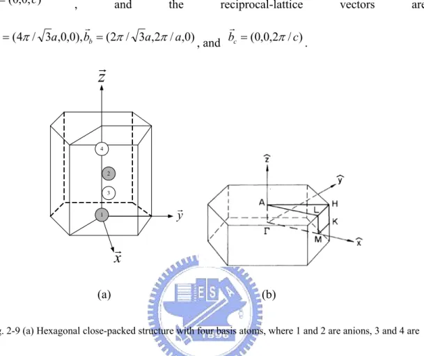
(40) determinations of the symmetry properties of a wide range of tensor quantities in various crystal symmetries. Poulet and Mathieu [5] give the fullest account of the calculation of selection rules and symmetry properties of second-order susceptibilities for inelastic light scattering. These calculations are not repeated here, but the main results for the 32 crystal point groups are set out in Ref. 5, which were divided into three parts, for crystals with biaxial, uniaxial, and isotropic dielectric properties. GaN-, AlN- and InN-based materials are highly stable in the hexagonal wurtzite structure (uniaxial) although they can be grown in the zinc blende phase and unintentional phase separation and coexistence may occur. The wurtzite crystal structure belongs to the space group zone-center optical modes are A1, 2B1, E1 and 2E2.. C6v4 and group theory predicts. The A1 and E1 modes and the two E2. modes are Raman active while the B modes are silent.. The A and E modes are polar,. resulting in a splitting of the LO and TO modes (Hayes and Loudon, 1978 [6]). The Raman tensors for the wurtzite structure are as follows:. 22.
(41) ⎛ a 0 0⎞ ⎜ ⎟ ⎜ 0 a 0⎟ ⎜ 0 0 b⎟ ⎝ ⎠. A1 (z) mode,. ⎛0 0 c⎞ ⎜ ⎟ ⎜ 0 0 0⎟ ⎜ c 0 0⎟ ⎝ ⎠. E1 (x) mode,. ⎛ 0 0 0⎞ ⎜ ⎟ ⎜0 0 c⎟ ⎜ 0 c 0⎟ ⎝ ⎠. E1 (y) mode,. ⎛f ⎜ ⎜0 ⎜0 ⎝. 0 −f 0. 0⎞ ⎛ 0 ⎟⎜ 0⎟ ⎜ − f 0 ⎟⎠ ⎜⎝ 0. −f 0 0. 0⎞ ⎟ 0⎟ 0 ⎟⎠. E2 mode.. Here x, y or z in brackets after an irreducible representation indicates that the vibration is also infra-red active and has the direction of polarization indicated. Such vibrations occur only in piezo-electric crystals (i.e. crystals with no center of inversion symmetry). In crystals which do have a center of inversion symmetry, only even-parity vibrations, whose representations have a subscript g, can be Raman active and only odd-parity (subscript u) vibrations can be infrared active.. This fact leads to the important. complementary nature of infra-red absorption and Raman effects measurements. Directly above each irreducible representation is a matrix, which gives the non-vanishing μ components of the Raman tensor, i.e., of α ρσ , μ or Rρσ .. The different elements of the. matrices are the nine components of the tensor obtained by allowing both ρ and σ to take 23.
(42) on the values x, y and z.. Here x, y, and z are the crystal principal axes chosen to be. identical with the principal axes x1, x 2 and x3 defined for all the crystal classes by Nye. The component μ of the phonon polarization for the case of infrared-active vibrations is the quantity given in brackets after the irreducible representation symbol.. Fig. 2-3 Phonon dispersion curves for ZnO crystal of wurtzite structure. (after Calleja et al. [7]). The vibrational modes in ZnO wurtzite structures are given in Figure 2-3. At the Γ point of the Brillouin zone, it can be seen that the existence of the following optic phonon modes:. A1+2B1+E1+2E2; A1 and E1 modes are both Raman and infrared active; and B1. (low) and B1 (high) modes are silent.. For the lattice vibrations with A1 and E1. 24.
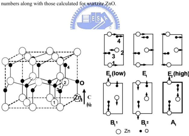
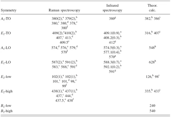
(43) symmetries, the atoms move parallel and perpendicular to the c axis, respectively. The low-frequency E2 mode is associated with the vibration of the heavy Zn sublattice, while the high-frequency E2 mode involves only the oxygen atoms.. The displacement vectors. of the phonon normal modes are illustrated in Fig. 2-4. In the case of highly oriented ZnO films, if the incident light is exactly normal to the surface, only A1 (LO) and E2 modes are observed, and the other modes are forbidden according to the selection rules.. Raman. Table 2-1 gives a list of observed zonecenter optical-phonon wave. numbers along with those calculated for wurtzite ZnO.. Fig. 2-4 Displacement vectors of the phonon modes in ZnO wurtzite structure. (after Jephcoat et al. [8]). 25.
(44) Table 2-1 Phonon mode frequencies of wurtzite ZnO at the center of the Brillouin zone obtained from infrared spectroscopic ellipsometry and Raman scattering measurements in comparison with theoretical predictions [1].. 2.2 Excitons-related emissions Optical properties of a variety of forms of ZnO, including ZnO nanostructures, have been studied by PL spectroscopy. ZnO. nanostructures. have. The majority of the reported luminescence spectra of. been. measured. at. room. temperature,. although. variable-temperature PL studies have been performed on some of the samples. Room-temperature PL spectra of ZnO typically consist of a UV emission and possibly 26.
(45) one or more visible bands due to defects and/or impurities.. 2.2.1 UV Emission [1, 29] Low-temperature. PL. measurements. of. different. nanostructures,. such. as. nanowire/nanowall systems, nanosheets, nanowalls, nanowires, nanorods, faceted nanorods, nanoparticles, nanoblades and nanoflowers have been reported [9-13].. Low. temperature (4-10 K) PL spectra of ZnO typically exhibit several peaks (labeled I0-I11), which correspond to bound excitons [14].. An example of a low-temperature PL. spectrum of a ZnO sample exhibiting a number of bound-exciton peaks is shown in Fig. 2-5.. Fig. 2-5 Bound-excitonic region of the 10 K PL spectrum for the forming gas annealed ZnO substrate [15]. 27.
(46) The number of observed bound-exciton peaks in ZnO nanostructures is typically lower than that in ZnO single crystals. An example of a low-temperature and their capture cross sections, [15] variable-temperature PL measurements can provide useful information about the optical and structural properties of ZnO.. However, the. assignment of the bound-exciton peaks in ZnO is, in general, controversial for all forms of the samples, namely, ZnO single crystals, epitaxial films, and nanostructures. For example, it was proposed that the emission lines I5 to I11 in the lower part of the energy spectrum can be attributed to excitons bound to neutral acceptors [16].. However, other. reports in the literature attributed some of these lines to donor bound excitons [15, 17]. The chemical identity of the donors and acceptors responsible for different bound-exciton lines still remains unclear (for a complete list of the bound-exciton peaks generally observed in ZnO, and a summary of the possible identification of the donors and acceptors, see Ref.1 and Ref.15]).. One of the commonly observed bound-exciton lines. in ZnO nanostructures is the I4 line at near the 3.3628 eV [18].. This emission is. typically attributed to the donor bound exciton, and the donor has been identified as hydrogen [14, 19]. Theoretical calculations predict hydrogen to be a shallow donor in ZnO and it is reasonable to expect that an unintentional incorporation of hydrogen could frequently happen in ZnO nanostructure synthesis. 28. While in general there is a.
(47) consensus in assigning the I4 line to hydrogen donors [14, 19], the chemical identity of donors responsible for other donor bound-exciton lines remains unclear. For the acceptor bound excitons, the most commonly reported peak is located at 3.3564 eV. This peak is commonly attributed to excitons bound to Na or Li acceptors [1].. Alkali metals are predicted to produce shallow acceptors on the cation site, but the. experimental results demonstrate that doping with group Ι ions produces complex results [20]. However, other acceptor levels have also been proposed, such as an acceptor complex involving a N impurity on an O site [21]. donor bound exciton instead.. Some authors attribute this line to a. Bound-exciton lines I6, I8, and I9 have been assigned to. excitons bound to Al, Ga, and In donors, respectively [14].. On the other hand, Thonke. et al. [18] proposed that the weak 3.357 eV line corresponds to the acceptor bound exciton, while the I8 line at 3.3597 eV was found to be a donor bound-exciton line. In addition to commonly observed acceptor bound-exciton lines, emission at 3.332 eV (labeled as Ia) was recently observed in low-temperature PL spectra of ZnO epilayers grown on CaF2(111) [22].. Since this peak occurs in the spectral region where. two-electron satellites (TES) of donor bound-exciton peaks are expected to occur [18], careful examination of the peak position in respect to known bound-exciton positions and 29.
(48) expected TES peaks (see Ref. [14] for the positions of TES lines for different bound-exciton peaks) is necessary. In addition, the occurrence of peak near 3.333 eV may indicate excitons bound to structural defects [14].. Therefore, further work is. needed for conclusive identification of the origin of different bound-exciton lines in ZnO. The assignment of several bound-exciton lines, especially I9, is still controversial and conclusive chemical identification of the majority of donors and acceptors has not been accomplished. At low temperatures, in addition to bound-exciton peaks, TES transitions can be observed in the spectral region 3.32–3.34 eV [15].. These transitions correspond to a. radiative recombination of donor bound excitons, which leaves the donor in an excited state.. Thus, they are located at energy lower by an amount equal to the difference. between the first excited and ground states of the donor, so that their position in respect to the donor bound-exciton peaks can be used to estimate donor-binding energies.. Finally,. low-temperature PL spectra can also contain donor-acceptor pair transitions and longitudinal optical (LO) phonon replicas. phonon replicas can typically be observed.. The first-, second-, and third-order LO The LO phonon energy can be determined. from the separation between the exciton peaks and their LO phonon replicas, and for ZnO it is 71-73 meV. Since donor-acceptor pair transitions and some of the LO phonon 30.
(49) replicas occur in the same spectral region (3.218-3.223 eV), care needs to be taken in assigning the peaks observed in this region. With regard to the temperature dependence of the observed peaks, a red shift of the free-exciton emission with increasing temperature occurs.. The intensity of the. bound-exciton peaks and the LO phonon replicas decreases with increasing temperature, and only free-exciton emission can be observed at room temperature.. In ZnO epilayers,. free-exciton emission was found to dominate the spectra above ~80 K [23].. Similar. behavior, with the disappearance of bound-exciton peaks above 150 K, was also observed in ZnO single-crystal samples. The bound-exciton line for ZnO nanoparticles embedded in alkali halide crystals also disappeared at ~125 K [24].. The exact temperature at. which the bound-exciton line will disappear depends on the identity of the donors or acceptors, since different donors/acceptors will be thermally ionized at different temperatures.. It should be noted that in the case of donor-acceptor pair transition,. disappearance of this peak with increasing temperature can be accompanied by the appearance of acceptor bound-exciton peaks if the acceptors are thermally ionized at higher temperature than the donors [25]. However, what all ZnO samples (single crystals, films, and nanostructures) have in common is the disappearance of bound-exciton peaks at temperatures in the range 50-150 31.
(50) K, while at room temperature only free-exciton emission is observed. The presence of free-exciton emission at low temperatures, as well as a distinction between A and B exciton peaks, is usually considered to indicate high quality in ZnO samples.. It should. be noted that this criterion for sample quality is less arbitrary than the ratio between UV and defect emission, which is sometimes used to estimate sample quality, and which is dependent on excitation area and power. Additionally, biexciton emission was observed at ~77 K in high-quality epitaxial ZnO films and nanopowder [23, 26].. The biexciton. binding energy was estimated to be 15 meV. Clear observation of free-exciton and biexciton lines at low temperatures is usually considered as an indication of very good sample quality. In room-temperature PL spectra, some variation of the position of the PL peak can be observed for different nanostructures.. This is illustrated in Fig. 2-6, where different. UV peak positions (387 nm for tetrapods, 381 nm for needles, 397 nm for nanorods, 377 nm for shells, 379 nm for faceted rods, and 385.5 nm for ribbons/combs) can be observed. These differences in the peak positions of individual nanostructures, which are sufficiently large so that there could be no quantum confinement effects, indicate that there is likely a different explanation for the variation in the band-edge emission in ZnO nanostructures reported in different studies. Even though quantum confinement has 32.
(51) been proposed as a cause of the blue shift of the band-edge emission with decreasing size, any shift due to quantum confinement in nanocrystals with diameters of 57, 38, and 24 nm were not likely considering the fact that the Bohr radius of ZnO is 2.34 nm [27].. Fig. 2-6 Room-temperature PL spectra of various nanostructures in the UV range [29]: 1) Tetrapods, 2) needles, 3) nanorods, 4) shells, 5) highly faceted rods, 6) ribbons/combs.. One possible reason for the variations in the position of the band-edge emission in various ZnO nanostructures with relatively large dimension is different concentrations of native defects.. Since the defect density on the surface is higher than in the bulk, spectral. shifts due to different defect concentrations are expected to occur in nanostructures with different sizes due to different surface-to-volume ratios [28].. The fact that the decay. times in time-resolved PL from ZnO nanorods are size dependent is in agreement with 33.
(52) the assumption of different defect levels/concentrations for structures with different surface-to-volume ratios.. Thus, the defects could affect the position of the band-edge. emission as well as the shape of the luminescence spectrum.. Although there have been. several reports with strong UV and weak defect emission in ZnO nanostructures, in some cases only defect emission is observed or the UV emission is much weaker compared to the defect emission.. Therefore, clarifying the origins of different defect emissions is an. important issue. However, it should be noted that the ratio of the intensity of UV and defect emission is dependent on the excitation density, as well as the excitation area. Thus, the ratios of these two emissions cannot be used as an absolute determining factor of the crystalline quality of ZnO, although they are useful in comparing the quality of different samples when the measurements are performed under identical excitation conditions.. 2.2.2 Defect Emission [29] Room-temperature PL spectra from ZnO can exhibit a number of different peaks in the visible spectral region, which have been attributed to the defect emission. Emission lines at 405, 420, 446, 466, 485, 510, 544, 583, and 640 nm have been reported. Several calculations of the native defect levels in ZnO have been reported [30, 31] as summarized 34.
(53) in Fig. 2-7. An example of defect emissions (normalized PL spectra) from different ZnO nanostructures is shown in Fig. 2-8.. Fig. 2-7 Illustration of the calculated defect energy levels in ZnO [29].. Green emission is the most commonly observed defect emission in ZnO nanostructures, similar to other forms of ZnO. The intensity of the blue-green defect emission was found to be dependent on the nanowire diameter, [32, 33] but both increased [32] and decreased [33] defect emission intensity with decreased wire diameter were reported.. 35.
(54) Fig. 2-8 Room-temperature PL spectra of different nanostructures [29]:. 1) Tetrapods, 2) needles, 3). nanorods, 4) shells, 5) highly faceted rods, 6) ribbons/combs.. Several hypotheses have been proposed:. Green emission is often attributed to. singly ionized oxygen vacancies, although this assignment is highly controversial. Other hypotheses include antisite oxygen, which was proposed by Lin et al. [31] based on the band structure calculations. and zinc interstitials [34].. Green emission was also attributed to oxygen vacancies. Cu impurities have been proposed as origin of the green. emission in ZnO. Blue-green defect emission was also reported in Cu doped ZnO nanowires [35]. Although Cu was identified as a possible cause of green emission in ZnO, this cannot explain the defect emission in all ZnO nanostructure samples, especially those where defect emission exhibits strong dependence on annealing temperature and 36.
(55) atmosphere which would be more consistent with an intrinsic defect rather than Cu impurity. Other hypotheses include various transitions related to intrinsic defects, such as donor-acceptor transitions, recombination at Vo** centers (where these centers are generated by surface trapping of photogenerated holes, followed by recombination with electron in an oxygen vacancy Vo* [36]), zinc vacancy [37], and surface defects [38]. Although the singly ionized oxygen vacancy is a commonly cited hypothesis, which is supported by reports of the enhancement of the green defect by annealing at temperatures above 600℃ (attributed to out-diffusion of O), this assignment has been questioned recently. On the other hand, while the Zn vacancy hypothesis is supported by the study of the effect of O and Zn implantation [39], a blue rather than green emission would be expected based purely on the theoretically predicted energy levels for Zn vacancy. Therefore, the origin of the green emission is still an open and controversial question and the identification of the exact origin of this emission requires further study.. While the. type of defect responsible for the green emission has not yet been conclusively identified, there is convincing evidence that it is located at the surface. It was shown that coating ZnO nanostructures with a surfactant suppressed green emission.. Polarized. luminescence experiments from aligned ZnO nanorods also indicated that green emission originated from the surface of the nanorods [40]. 37. The surface recombination layer.
(56) responsible for visible emission in ZnO nanowires was estimated to be ~30 nm in thickness.. Also, the possible presence of Zn(OH)2 at the surface, especially for. nanostructures prepared by solution methods, could affect the emission spectra from ZnO nanostructures. Yellow defect emission is also commonly reported in ZnO nanostructures [41, 42], and it represents a common feature in samples prepared from aqueous solutions of zinc nitrate hydrate and hexamethylenetetramine. This emission is typically attributed to oxygen interstitial, although a Li impurity represents another possible candidate. The deep levels responsible for green and yellow emissions were found to be different; unlike the defect responsible for the green emission, the defect responsible for the yellow emission is not located at the surface. In addition to green and yellow emissions, orange-red emissions are often also observed. Fan et al. [43] reported that the visible emission in ZnO dendritic wires and nanosheets consisted of two components centered at ~540 and ~610 nm.. The intense. visible emission in ZnO nanosheets was tentatively attributed to surface dislocations. Orange-red emission at ~626 nm in ZnO nanorods was attributed to oxygen interstitials. In addition, orange emission at ~640-650 nm in ZnO needles and nanowires [44] was proposed to be due to oxygen-rich samples, in agreement with a previous study on ZnO 38.
數據
![Fig. 1.2 Representative scanning electron microscopy images of various ZnO nanostructure morphologies [32-34]](https://thumb-ap.123doks.com/thumbv2/9libinfo/8421096.180522/24.892.174.697.158.509/representative-scanning-electron-microscopy-images-various-nanostructure-morphologies.webp)

+7
![Fig. 2-5 Bound-excitonic region of the 10 K PL spectrum for the forming gas annealed ZnO substrate [15]](https://thumb-ap.123doks.com/thumbv2/9libinfo/8421096.180522/45.892.157.726.523.1048/fig-bound-excitonic-region-spectrum-forming-annealed-substrate.webp)
![Fig. 2-6 Room-temperature PL spectra of various nanostructures in the UV range [29]: 1) Tetrapods, 2)](https://thumb-ap.123doks.com/thumbv2/9libinfo/8421096.180522/51.892.130.751.368.697/fig-room-temperature-spectra-various-nanostructures-range-tetrapods.webp)
![Fig. 2-7 Illustration of the calculated defect energy levels in ZnO [29].](https://thumb-ap.123doks.com/thumbv2/9libinfo/8421096.180522/53.892.182.725.332.730/fig-illustration-calculated-defect-energy-levels-zno.webp)
![Fig. 3-1 Schematic of the rotes that one could follow within the scope of sol-gel processing [8]](https://thumb-ap.123doks.com/thumbv2/9libinfo/8421096.180522/78.892.193.694.377.744/fig-schematic-rotes-follow-scope-sol-gel-processing.webp)
相關文件
For example, Liu, Zhang and Wang [5] extended a class of merit functions proposed in [6] to the SCCP, Kong, Tuncel and Xiu [7] studied the extension of the implicit Lagrangian
Then, we tested the influence of θ for the rate of convergence of Algorithm 4.1, by using this algorithm with α = 15 and four different θ to solve a test ex- ample generated as
Numerical results are reported for some convex second-order cone programs (SOCPs) by solving the unconstrained minimization reformulation of the KKT optimality conditions,
Particularly, combining the numerical results of the two papers, we may obtain such a conclusion that the merit function method based on ϕ p has a better a global convergence and
Then, it is easy to see that there are 9 problems for which the iterative numbers of the algorithm using ψ α,θ,p in the case of θ = 1 and p = 3 are less than the one of the
By exploiting the Cartesian P -properties for a nonlinear transformation, we show that the class of regularized merit functions provides a global error bound for the solution of
volume suppressed mass: (TeV) 2 /M P ∼ 10 −4 eV → mm range can be experimentally tested for any number of extra dimensions - Light U(1) gauge bosons: no derivative couplings. =>
For ASTROD-GW arm length of 260 Gm (1.73 AU) the weak-light phase locking requirement is for 100 fW laser light to lock with an onboard laser oscillator. • Weak-light phase
