The increasing complexity and miniaturization of modern inte-grated circuits (ICs) demand a higher device yield and hence lower defect density in the active region of silicon devices.1For a deep-submicrometer device, a single metal precipitate could cause a dis-tortion of electrical properties and result in a faulty IC.2-5For exam-ple, metals can degrade the dielectric properties of gate oxide, caus-ing premature breakdown. They can also diffuse into the bulk of the silicon substrate, resulting in increased junction leakage as well as reduced minority carrier lifetime. Therefore, a better knowledge of the diffusion route and behavior of impurities introduced into the sil-icon substrate during device fabrication could help to control conta-mination and thus promote circuit yield.
The control of fabrication processes involved in device manufac-turing becomes more and more crucial due to increasing complexity of the materials and tools. Among them, lithography plays a very important role because it is applied repeatedly to the wafer surface during device manufacturing. Many lithographic models have been developed and applied for the photoresist profile simulation,6-8 how-ever, to the best of our knowledge, the effects of impurity segrega-tion and diffusion of Mn and Zn impurities in the deep ultraviolet (DUV) photoresist have not yet been reported. The behavior of metallic contaminants in DUV photoresist and their migration into the underlying substrate is of eminent importance, because proper control of elemental impurity levels in the “high-purity” DUV pho-toresist would be very crucial for fast proliferation of DUV photore-sist in the IC industry in the coming years.9Although it is always safer to demand an unnecessarily high degree of purity for DUV photoresist (i.e., 50-100 ppb for i-line and 10-30 ppb for DUV pho-toresist), the resulting cost would be extremely high and unneces-sary. As this would require tedious sample pretreatment procedures, including matrix decomposition by hot plate or microwave oven, separation, preconcentration, and control of sample handling and analytical environment.10-12 Therefore, a systematic study of the impurity diffusion behavior from DUV photoresist into the underly-ing substrate is technologically important and urgent from the view-point of setting the proper standard level of tolerable impurities in DUV photoresist for ultralarge-scale integrated (ULSI) industrial application.
To evaluate the ratios of metallic impurities diffusing from DUV photoresist into the underlying substrate during lithographic process-ing, e.g., bakprocess-ing, various analytical methods are required for de-termining the impurities in the resist layer and in the underlying
sub-strate.13Methods that have been developed for detecting Mn and Zn impurities include graphite furnace atomic absorption spectrometry (GFAAS), inductively coupled plasma mass spectrometry (ICP-MS), total reflection X-ray fluorescence (TXRF) spectrometry, and sec-ondary ion mass spectrometry (SIMS).14-17However, these methods suffer from the shortcomings11,18,19of the need to develop the de-composition method for the photoresist. They also require high sen-sitivity for the instrument and are cumbersome in determining spec-troscopic interference. In addition, the required blank control can seriously affect the analytical reliability during measurement.20,21
The radioactive tracer technique22-24has proved very suitable for studying element migration in materials, environment, and biochem-istry. In semiconductor fabrication, the well-known RCA cleaning method,25 universally applied in wafer processing for removing impurities from silicon wafers, was originally developed based on the radioactive tracer method by Kern and Puotinen in 1970. It is still in wide use today and forms the basis of many so-called modified RCA cleaning methods for wafer cleaning. The effectiveness of the RCA cleaning method was first established by deliberately contam-inating the wafer surface with radioactive nuclides of 64Cu and 198Au. Gamma radioactivity was then recorded before and after RCA cleaning to monitor cleaning efficiency. The advantages of the radioactive tracer technique are well recognized; they include high throughput, easy operation, interference-free from stable isotope, and reliability. Despite the versatility of the radioactive tracer tech-nique, it has not yet been applied to study the impurity behavior dur-ing lithographic and subsequent cleandur-ing processes.
In this work, the radioactive tracer method is first introduced to investigate the migration ratio of Mn and Zn impurities from DUV photoresist into the underlying substrate. The effects of various bak-ing temperatures are evaluated. Furthermore, a diffusion model, to-gether with a newly proposed parameter, K, is suggested to describe the impurity diffusion in the photoresist layer and its subsequent dif-fusion into the underlying substrate. In addition, by using the same radioactive tracer method, the impurity cleaning efficiency of vari-ous wet chemical cleaning recipes is also evaluated in this work. Possible mechanisms relevant to impurity diffusion associated with various underlying substrates are discussed.
Experimental
Materials.—p-Type <100> wafers with 15 cm diam were
passi-vated with various films (i.e., polysilicon, silicon dioxide, silicon nitride, and nonpassivated or bare silicon control). They were cut into 2 3 2 cm pieces to serve as test samples. The samples were then
Characterization and Modeling of Out-Diffusion of Manganese and Zinc
Impurities from Deep Ultraviolet Photoresist
Mei-Ya Wang,
aFu-Hsiang Ko,
b,zTien-Ko Wang,
aChin-Cheng Yang,
band Tiao-Yuan Huang
baDepartment of Engineering and Systems Science, National Tsing Hua University, Hsinchu 300, Taiwan bNational Nano Device Laboratories, National Chiao Tung University, Hsinchu 300, Taiwan
The radioactive tracer technique was applied to investigate the out-diffusion of manganese and zinc impurities from deep-ultravi-olet (DUV) photoresist. Two important process parameters, viz., baking temperature and the type of substrate (i.e., bare silicon, polysilicon, oxide, or nitride), were evaluated. Our results indicated that diffusion ratios were all below 6%, irrespective of the sub-strate type and baking temperature. The subsub-strate type did not appear to strongly affect the metallic impurity out-diffusion from DUV photoresist. However, solvent evaporation was found to have a significant effect on impurity diffusion. A new model, togeth-er with a new paramettogeth-er, was proposed to describe the out-diffusion behavior of impurities from DUV photoresist. This model could explain the diffusion ratio of metallic impurities in photoresist layers under various baking conditions. The effectiveness of various wet cleaning recipes in removing metallic impurities such as manganese and zinc was also studied. It was found that (i) bath life due to temperature change can considerably affect the cleaning efficiency, and (ii) hot water immersion can effectively dissolve the impurities from the wafer surface.
© 1999 The Electrochemical Society. S0013-4651(98)11-080-7. All rights reserved. Manuscript submitted November 25, 1998; revised manuscript received June 3, 1999.
S0013-4651(98)11-080-7 CCC: $7.00 © The Electrochemical Society, Inc. processed through various lithographic and cleaning processes to
study the contaminants as introduced by the lithographic process and the effectiveness of removing these contaminants by the subsequent cleaning method. Carrier-free radioactive tracers from DAMRI (France) were used in this study. Their composition was 37 mg/g of 54MnCl
2(0.838 M Bq/g) and 10 mg/g of 65ZnCl2(0.857 M Bq/g) in 0.1 N hydrogen chloride solution.
The photoresist used in this work was SEPR-401H positive-type photoresist from Shin-Etsu Chemical (Japan). This particular pho-toresist was chosen because it is a popular phopho-toresist for gate and metal-layer applications in state-of-the-art ULSI manufacturing. It can be used in KrF excimer-laser exposure at 248 nm wavelength. The photoresist stripper was 1-methyl-2-pyrrolidone (NMP) from E. Merck (Germany).
Various popular wet cleaning recipes, including SC1, H2O, SC2, DHF (dilute hydrogen fluoride) SPM (sulfuric acid-hydrogen perox-ide mixture), and BOE (buffered oxperox-ide etch), were studied in this work. The chemical composition of SC1 solution was ammonium hydroxide, hydrogen peroxide, and water with a volume ratio of 1:1:5. The chemical composition of SC2 solution was hydrogen chloride, hydrogen peroxide, and water with a volume ratio of 1:1:6. The chemical composition of DHF solution was hydrogen fluoride and water with a volume ratio of 1:50. The chemical composition of SPM solution was sulfuric acid and hydrogen peroxide with a vol-ume ratio of 4:1. The chemical composition for BOE solution was hydrogen fluoride and ammonium fluoride with a volume ratio of 1:6. All reagents used were of analytical or higher grade from E. Merck. Water was treated by reverse osmosis and mixed-bed ion exchange to ensure a resistivity of at least 18 MV cm.
Film-formation process.—To prepare different underlying
sub-strates for study, films of polysilicon, silicon oxide, and silicon nitride were deposited on various starting silicon wafers by low-pressure chemical vapor deposition (LPCVD) in a quartz reactor. Polysilicon film was deposited with silane gas (SiH4) in 60 sccm and 6208C. Silicon oxide layer was grown by wet oxidation with a mix-ture gas of hydrogen (8 slm) and oxygen (4999 sccm) at 9788C. Sil-icon nitride film was deposited with a mixture gas of ammonium (130 sccm) and dichlorosilane (SiH2Cl2, 30 sccm) at 7808C.
Afterward, wafers were cut into 2 3 2 cm pieces to serve as test samples. Photoresist layer was then coated on each sample. This was accomplished by first holding the test sample on the chuck by vacu-um and then 1 mL of radioactive photoresist was dispensed on the sample surface by the pipette. The coating process was performed by spinning at 1500 rpm for 0.5 min. Samples were then split to bake at 80, 100, and 1208C for 2 min by a hot plate.
Film thickness was measured using either a Nanospec optical film thickness monitor manufactured by Nanometrics Incorporated (USA) or an N&K analyzer (USA).
Radioactive tracer experimental procedure.—To prepare the
radioactive photoresist, one volume of diluted radioactive tracer (0.005 N) was mixed with five volumes of photoresist, and the radioactive photoresist solution was well shaken to ensure homoge-neous distribution. The radioactive photoresist was then applied to the test sample by the spin-coating process as mentioned previously. After solvent evaporation, the test sample was counted by a high-res-olution gamma-ray spectrometer. The counting system consists of an HPGe detector coupled with a multichannel analyzer (Canberra AccuSpec) and the usual electronics. The energy resolution of the system was 2.4 keV at 1332 keV. The intensity of the gamma ray for 54Mn (t1/25 312.2 d) and 65Zn (t1/25 243.9 d) was monitored at 1115.5 and 834.8 keV, respectively. After counting, the photoresist layer was removed by dipping in a 100 mL NMP solution at 608C for 5 min and dried by a hot plate. The radioactivity of the impuri-ties left on the wafer was then checked by the same HPGe detection system. The diffusion ratio of Mn and Zn impurities from photore-sist into the underlying substrate was determined by the ratio of the time-averaged counts before and after the photoresist stripping.
To study the effectiveness of wet cleaning recipes, radioactive tracer solution was added to the test samples. Then the samples were dried on a hot plate at 508C. The radioactivity was recorded by the gamma-ray counting system mentioned previously. Afterward, test samples were immersed in the respective wet solutions, i.e., SC1, H2O, SC2, DHF, SPM, and BOE, at various temperatures for 5 min to dissolve or desorb the impurities. Samples were then taken out of the solution, immersed in room-temperature water solution to remove the residual chemical, and dried by hot plate. The radioac-tivity emitted from the residual impurities was measured again. The effectiveness of various wet cleaning recipes could thus be assessed based on the ratio of the radioactivities counted before and after the wet chemical immersion.
Results and Discussion
Out-diffusion of Mn and Zn from DUV photoresist.—Impurities in DUV photoresist.—Various possible behaviors, including
diffu-sivity, solubility, precipitation, and gettering, have been proposed previously for the impurities existing in the silicon substrate during thermal treatment.26,27However, little has been reported about the behavior of metallic impurities in DUV photoresist.
Since the photoresist layer after baking is an amorphous polymer, it is suitable to use the diffusion model for predicting impurity be-havior. Theoretically, the out-diffusion of impurity from photoresist should continue until equilibrium is reached. However, two features should be noted in describing the diffusion process. First, the impu-rity diffusion coefficient in the photoresist is normally much higher than that in the underlying substrate. Second, the underlying sub-strate can act as a gettering-like region; therefore, the impurity dif-fusing from the photoresist would mostly appear in the upper region of the substrate (<20 nm). 27
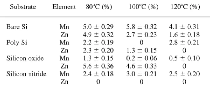
Table I summarizes the diffusion ratios of Mn and Zn impurities from DUV photoresist into various underlying substrates for three dif-ferent baking temperatures (i.e., 80, 100, and 1208C). It can be seen that the (percentage) diffusion ratios are all below 6%, irrespective of the underlying substrates and baking temperatures. This shows that both Mn and Zn have low diffusion ability in the DUV photoresist at the normal baking temperatures used in this study. It is generally anticipated that the diffusion may be promoted by elevating the reac-tion temperature. However, as can be seen from Table I, the diffusion ratio does not show this dependency. The data for Zn decreases with temperature regardless of substrate, whereas Mn goes up then down for substrates of bare Si and silicon nitride, and down then up for sub-strates of poly Si and silicon oxide. This tendency can be explained by the metallic ion migration mechanism proposed as follows.
It is reasonable to consider that metallic ion can be solvated with the residual H2O or photoresist solvent to form M(H2O)xn1or M(sol-vent)xn1in the photoresist layer. As the film is heated, two pathways are possible, as illustrated in Fig. 1a. The baking temperature induces the metallic ion to move toward the substrate, while the sol-vated H2O or solvent evaporates in the opposite direction. The net driving force of impurity changes with temperature and the impuri-ty diffusion can be classified into four impuri-types, as shown in Fig. 1b. Type I describes the condition when the effect of impurity migration
Table I. The diffusion ratio for impurities transported from DUV photoresist into underlying substrates at various baking temperatures. Substrate Element 808C (%) 1008C (%) 1208C (%) Bare Si Mn 5.0 6 0.29 5.8 6 0.32 4.1 6 0.31 Zn 4.9 6 0.32 2.7 6 0.23 1.6 6 0.18 Poly Si Mn 2.2 6 0.19 0 2.8 6 0.21 Zn 2.3 6 0.20 1.3 6 0.15 0 Silicon oxide Mn 1.3 6 0.15 0.2 6 0.06 0.5 6 0.10 Zn 5.6 6 0.36 4.6 6 0.33 0 Silicon nitride Mn 2.4 6 0.18 3.0 6 0.21 2.5 6 0.20 Zn 0 0 0
dominates while the effect of H2O or solvent evaporation is negligi-ble; as a result, the diffusion ratio increases as temperature goes up. Type II is H2O or solvent evaporation dominates while the effect of impurity migration is insignificant; therefore, the diffusion ratio decreases as temperature goes up. Type III has a turnover tempera-ture Ti. In the temperature region when T < Ti, the impurity migra-tion is dominating and the net diffusion behaves like type I; where-as, when T > Ti, it behaves like type II. Type IV shows the opposite tendency as compared with type III.
Based on the proposed model shown in Fig. 1, the experimental data appearing in Table I can be realized. The tendency of Mn diffu-sion for substrates of bare Si and silicon nitride can be attributed to type III, whereas for substrates of poly Si and silicon oxide it be-longs to type IV. It is interesting to find that Zn has type II diffusion regardless of the substrate type. The diffusion ratio for Zn in silicon nitride substrate is near null, which is a special case of type II. This indicates that H2O and solvent evaporation can effectively restrict the Zn impurity from reaching the substrate.
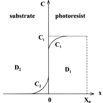
Diffusion model.—A semi-empirical diffusion model for the
migra-tion of metallic impurities from DUV photoresist into the silicon substrate is described in Fig. 2. The initial concentration of metallic impurity in the photoresist layer is assumed to be Ciat various cross sections. Equations 1 and 2, which describe the relationship for the impurity in the photoresist and the underlying substrate at time t and location x, can be expressed as follows
[1] ∂ ∂ ∂ ∂ C t D C x 1 1 2 1 2 5 [2] where C1and C2denote the concentrations of metallic impurity in the photoresist layer and the underlying substrate, respectively, and D1, D2are the diffusion coefficients for the metallic impurity in the photoresist and the substrate, respectively.
Two conditions are assumed for the diffusion equations. The ini-tial condition (t5 0) gives C15 Ciand C25 0. Afterward, a diver-gent behavior in the boundary condition is expected as diffusion pro-ceeds (t > 0). By assuming there is no accumulation or adsorption of the diffusing impurity at the interface, the interface boundary condi-tion gives at x5 0
[3] A solution to meet the diffusion model can easily be obtained by combining the semi-infinite medium assumption and the initial and boundary conditions.28The solutions are
[4]
[5] where k5 C2/C1(at x5 0) is the impurity segregation coefficient at the interface, erf(z) is the error function, and erfc(z) 5 1 2 erf(z). The semi-infinite medium assumption needs X0 > 4(D1t)1/2; it is valid only at relatively short diffusion time (X0is the thickness of the pho-toresist layer). This assumption of short impurity diffusion length can also be verified by the small percentage of diffusion ratio of ex-perimental results as in Table I. As diffusion proceeds, the impurity concentration at the interface (x = 0) remains constant at the values
[6] [7] C C k D D 1 2 1 1 2 0 ( ) ( / )/ 5 1 i 1 C kC k D D 2 2 1 1 2 0 ( ) ( / ) / 5 1 i 1 C kC k D D x D t 2 2 11 2 2 2 5 1 i 1 ( / ) / erfc C C k D D k D D x D t 1 2 1 1 2 2 11 2 1 1 2 5 1 1 i 1 ( / ) / ( / ) erf / D C x D C x 1 1 2 2 ∂ ∂ ∂ ∂ 5 ∂ ∂ ∂ ∂ C t D C x 2 2 2 2 2 5
Figure 1. (a) The effect of photoresist baking on impurity migration. (b) Four types of impurity diffusion.
Figure 2. Diffusion model for impurity migration from photoresist to substrate.
S0013-4651(98)11-080-7 CCC: $7.00 © The Electrochemical Society, Inc. The parameter K.—Figure 3 illustrates the relationship of
concen-tration gradient and location obtained by the semi-empirical model for the impurity of the underlying substrate and the photoresist layer. The concentration at the interface is always fixed at C1(0) and C2(0) as described by Eq. 6 and 7. In addition, this figure demonstrates the trend of impurity-concentration change as impurities diffuse from the photoresist layer, with initial concentration Ci, into the underly-ing substrate.
It is difficult to investigate the concentration gradient (C1or C2) for impurity in the photoresist or substrate by experimental measure-ment, while in this work the radioactive tracer method can easily obtain the diffusion ratio without systematic error. With this advan-tage, a proposed model is derived as follows.
The rate of impurity migration through the interface is depicted by
[8] The total amount of impurity diffusing into the substrate in time t can be obtained by integrating
[9]
where A denotes the total area which is coated with DUV photore-sist, and Q(t) is the number of impurities in unit area.
Since the total amount of impurity (QiA) in the experiment is
equal to CiX0A, the diffusion ratio of diffusant after the bake can be
expressed by the following
[10] with
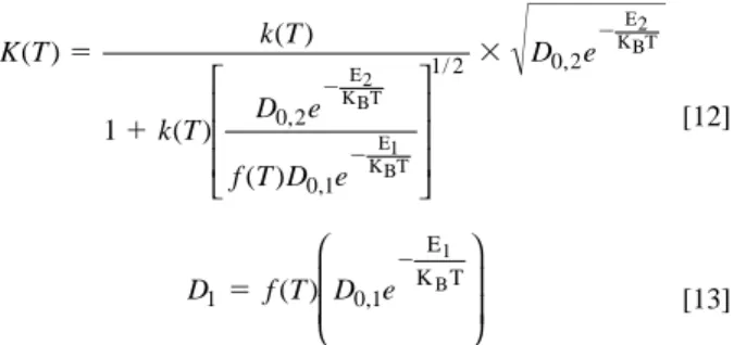
[11] The parameter K is first proposed and defined in the impurity diffusion model, which is dependent on substrate type, impurity structure, pho-toresist behavior, and temperature. In addition, the parameter is in-dependent of the baking time and impurity concentration. To describe the effect of temperature on K, the following equation is considered
K k k D D D 5 1 1 ( 2/ 1)1 2/ 2 Q t A Q A k k D D D t X t X K ( ) ( / ) / i 5 3 1 3 5 3 2 1 2 2 1 1 2 2 0 0 p p AQ t A Jdt kC k D D D t A t ( ) ( / ) / 5 5 3 1 3 3 0 2 11 2 2 2 1
∫
p i J D C x D C x kC k D D D t x x 5 2 5 2 5 1 5 5 1 1 0 2 2 0 2 1 1 2 2 1 ∂ ∂ ∂ ∂ ( i/ ) / p [12] [13] where k(T ) and f (T ) are unknown functions, T is the temperature in kelvin, D0,1and D0,2are the pre-exponential factors dependent on the vibration frequency of atoms in the lattice or interstitial sites, E1and E2are the binding energies at such sites, and kBis Boltzmann constant. The f (T ) function used to modify the impurity diffusion coefficient in the photoresist may be influenced by the heating type, evaporation pathway for photoresist solvent, and structure for photoresist layer.The D0,1e2E1/KBTterm in Eq. 13 increases with increasing tem-perature, while f (T ) might decrease with elevating baking tempera-tures, since the structure of the photoresist layer would become more condensed during baking. In addition, Fig. 1 also shows that H2O or solvent evaporation may also cause f (T ) to decrease with increasing temperature. Therefore, D1does not have to increase with increasing temperature. This is supported by the experimental observations pre-sented in Table I that the diffusion ratios for Mn and Zn impurities from DUV photoresist into the underlying substrate did not show significant temperature dependency.
Application of parameter K.—For the diffusion coefficient, the value reported in literature is always focused on high-temperature process-es (>6008C). Due to the substantially smaller value and restricted instrumental method, little is reported regarding the diffusion coeffi-cient at low temperature. Therefore, in this work we propose the parameter K to describe and simplify the diffusion model.
From Eq. 10, the parameter K can be rewritten as
[14] With this equation one may estimate the value of K for various types of impurity diffusion based on the experimental results (e.g., Table I). Small K represents low impurity diffusion, while large K represents high impurity diffusion. The resulting K values based on the data list-ed in Table I are illustratlist-ed in Table II. The change of K value with temperature might be relevant to the model proposed in Fig. 1. Fur-thermore, if we assume that the diffusion coefficient for the impurity in the photoresist is much larger than that in the solid silicon substrate (D1>> D2) at the normal baking temperature near 1008C, a simplified representation for the parameter K can also be obtained from Eq. 11
[15]
If either k or D2is found, the other parameter can also be predicted from Eq. 15 with K value known. The value of either k or D2can describe the out-diffusion of metallic ion from the photoresist.
Surface impurities in wet cleaning processes.—As reported, Mn and Zn impurities would migrate from the photoresist into the under-lying substrate during lithographic processing. Wet processing plays a fundamental role with respect to metallic contamination and its prevention. It has been reported29,30that the electrochemical segre-gation of metallic ions at the interface between cleaning solution and silicon substrate can be attributed to the following three possible mechanisms. The first is related to electronegativity. However, be-cause both Mn and Zn have lower electronegativity when compared with silicon (i.e., 1.65 and 1.55 on the Pauling scale for Mn and Zn,
K k D k D D k D 5 1 2 2 1 1 2 2 1 / > K Q t A Q A X t 5 ( ) 3 3 i 0 2 p D1 f T D0 1e 1 5 ( ) , 2 E K TB K T k T k T D e f T D e D e ( ) ( ) ( ) ( ) , , / , 5 1 3 2 2 2 1 0 2 0 1 1 2 0 2 E2 KBT E1 KBT E2 KBT
respectively, compared with 1.9 for silicon31), cations of Mn and Zn cannot be neutralized by taking electron from silicon. Therefore, electronegativity is ruled out as the segregation mechanism respon-sible for Mn and Zn. The second is related to the difference in the enthalpy of oxide formation for metal and silicon. Table III summa-rizes the standard molar enthalpy of oxide formation for various Mn and Zn complexes.31It indicates that manganese metasilicate, man-ganese orthosilicate, and zinc orthosilicate are the possible structures for postsegregation due to their lower enthalpy with respect to sili-con dioxide. The third sili-considers the effect of surface adsorption for the metal ions. This effect depends on the concentration of the metal
but also on the electrochemical potential state and solution pH con-dition. The latter two might be considered as the possible reasons for Mn and Zn in cleaning solution.
Six wet cleaning processes, i.e., SC1, H2O, SC2, DHF, SPM, and BOE, are commonly applied in wafer fabrication. Generally, the wet cleaning process is used to overcome the contamination problem after pattern definition. Mixtures of HF and NH4F, known as BOE, are used for etching oxide film to avoid loss of photoresist pattern that would not withstand the strong HF acid solution. Removal or cleaning of heavy organic, such as photoresist and its by-product, can be accomplished with SPM. However, the extent of residual metallic impurities remaining after BOE and SPM cleaning should still be carefully evaluated. This can help one understand the resid-ual impurity level by standard cleaning processes. The cleaning sequence DHF-H2O-SC1-H2O-SC2-H2O, modified from the con-ventional RCA clean, is well accepted because it shows better per-formance on light organic, particle, and metal cleaning. In this work, various wet processes were tested against their impurity removal efficiency by radioactive tracer technique. Among those prominent factors affecting the impurity removal efficiency, substrate type and the cleaning temperature were studied.
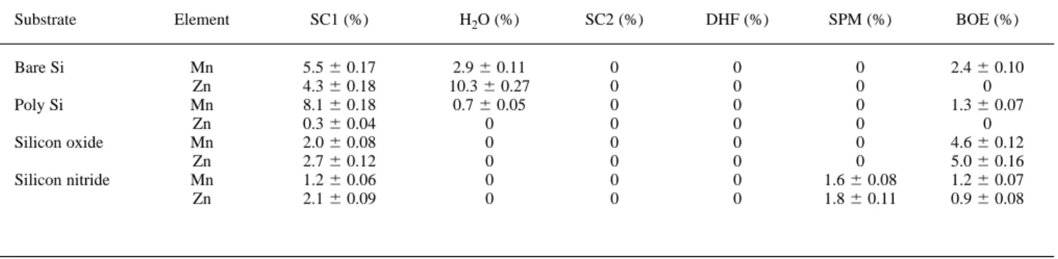
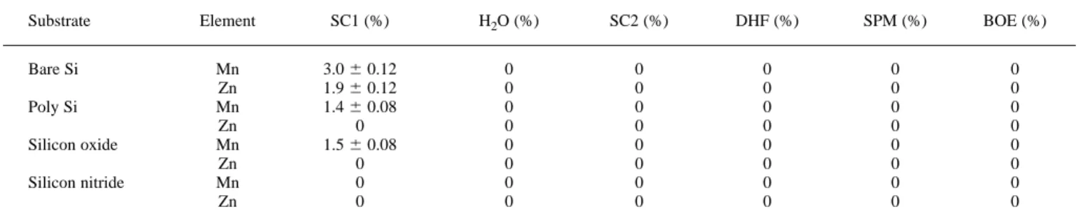
Tables IV to VI list the (percentage) remaining ratios of radioac-tive tracers Mn and Zn after 5 min dipping by various cleaning re-cipes at temperatures of 25, 47, and 828C, respectively. It can be seen that while SC2 and DHF are effective in impurity removal, irrespec-tive of the substrate types and solution temperature, residual Mn and Zn are found after an SC1 clean at room temperature for various sub-strates. This indicates that SC1 is the least effective, among all the cleaning solutions studied, for metallic impurity removal at room temperature.
Comparing Table IV (258C) with Table V (478C), the residual metallic impurities after SC1 treatment decrease at elevated treatment temperature, suggesting that the impurity diffusion between the sub-strate and SC1 solution increases at higher temperature. However, the cleaning efficiency at 828C appears to be poorer instead of better than that at 478C, as indicated by Table VI. This could be explained by the change of cleaning composition in the solution and the bath life of the chemical involved. The temperature strongly affects the lifetime of SC1, especially at higher temperature. It has been reported that hydrogen peroxide is thermally unstable and ammonium hydroxide is easily evaporated at higher temperature.32For SC1 reaction
mecha-Table II. K values for impurity diffusion at various baking temperatures.
808C 1008C 1208C Substrate Element (mm min21) (mm min21) (mm min21)
Bare Si Mn 0.0229 0.0265 0.0188 Zn 0.0224 0.0124 0.0073 Poly Si Mn 0.0101 — 0.0133 Zn 0.011 0.0062 — Silicon oxide Mn 0.0094 0.0014 0.0036 Zn 0.0404 0.0332 — Silicon nitride Mn 0.0075 0.0094 0.0078 Zn — — —
Table III. Standard molar enthalpy of oxide formation at 258C in kJ/mol.
Formula Name DH
MnO Manganese oxide 12385.2
MnSiO3 Manganese metasilicate 21320.9
Mn2SiO4 Manganese orthosilicate 21730.5
ZnO Zinc oxide 12350.5
Zn2SiO4 Zinc orthosilicate 21636.7
Zn(OH)2 Zinc hydroxide 12641.9
SiO2 Silicon dioxide 12910.7
Table IV. The remaining ratio of radioactive tracer after 5 min dipping by various cleaning recipes at 258C.
Substrate Element SC1 (%) H2O (%) SC2 (%) DHF (%) SPM (%) BOE (%)
Bare Si Mn 5.5 6 0.17 2.9 6 0.11 0 0 0 2.4 6 0.10 Zn 4.3 6 0.18 10.3 6 0.27 0 0 0 0 Poly Si Mn 8.1 6 0.18 0.7 6 0.05 0 0 0 1.3 6 0.07 Zn 0.3 6 0.04 0 0 0 0 0 Silicon oxide Mn 2.0 6 0.08 0 0 0 0 4.6 6 0.12 Zn 2.7 6 0.12 0 0 0 0 5.0 6 0.16 Silicon nitride Mn 1.2 6 0.06 0 0 0 1.6 6 0.08 1.2 6 0.07 Zn 2.1 6 0.09 0 0 0 1.8 6 0.11 0.9 6 0.08
Table V. The remaining ratio of radioactive tracer after 5 min dipping by various cleaning recipes at 478C.
Substrate Element SC1 (%) H2O (%) SC2 (%) DHF (%) SPM (%) BOE (%)
Bare Si Mn 0.3 6 0.04 16.7 6 0.29 0 0 0 1.0 6 0.06 Zn 0.5 6 0.06 20.0 6 0.42 0 0 0 0.9 6 0.08 Poly Si Mn 0 06.6 6 0.17 0 0 0 1.2 6 0.07 Zn 0 17.4 6 0.39 0 0 0 0.8 6 0.07 Silicon oxide Mn 0.4 6 0.04 0 0 0 0 0 Zn 0 0 0 0 0 0 Silicon nitride Mn 0 1.7 6 0.08 0 0 0 0 Zn 0 0 0 0 0 0
S0013-4651(98)11-080-7 CCC: $7.00 © The Electrochemical Society, Inc.
nisms, hydrogen peroxide serves as an oxidant, while ammonium hydroxide serves to etch away the grown oxide. With a constant com-position, the etching rate of various substrates by SC1 increases with elevating temperature. However, etching rate could be influenced and restricted by the effect of bath life.
H2O is generally used to rinse off chemicals from the previous cleaning step in wet wafer processing. It is found that the remaining ratios of Mn and Zn become zero for all underlying substrates at 828C, indicating that hot water immersion is very effective in dis-solving Mn and Zn impurities onto the wafer surface. It is noted that the diffusion length of these metals into the substrate is very small and therefore can easily be dissolved by hot water. However, it should be cautioned that this may be true only for Mn and Zn, other impurities may need further verification.
SC2 solution is found to be satisfactory as a cleaning recipe for removing Mn and Zn impurities. Our results clearly show that Mn and Zn impurities can be fully removed at all three different temperatures for any substrate. This can be explained by the chemical behavior of SC2 solution; its strong acid (H1) competition effectively replaces the metallic ions (i.e., Mn21, and Zn21) on the wafer surface. The same behavior can be found in the case of DHF solution. This result appar-ently is consistent with that of Anttila et al., who predict that the con-taminant of Zn should be removed in DHF,33despite the fact that thou-sands of particles may be added onto the wafer surface. The SPM solution also has a strong acid composition; therefore, the result is similar to SC2 and DHF, except for the case of silicon nitride at 258C. The cleaning ability of BOE solution to these metals is only efficient-ly found in 828C. At room temperature, part of the metal ions appears on the wafer. This can be explained by the formation of metal complex with ammonium, M(NH3)126 , which tends to adsorb on the surface of the substrate, but as the clean temperature increases, the driving force of ammonium evaporation (Fig. 1a) reduces the surface metal.
Conclusion
Characterization and modeling of impurity out-diffusion have been established to describe the mobility of manganese and zinc im-purities from DUV photoresist for baking temperatures ranging from 80 to 1208C. Only a limited amount of metallic impurity in the inter-face can diffuse. The diffusion ratio does not show strong baking tem-perature dependency. The diffusion behavior can be explained by the net driving force of impurity diffusion and solvent evaporation using the model proposed in this work.
The concentration level of metallic impurity in the photoresist and underlying substrate can be calculated with the proposed diffu-sion model. The diffudiffu-sion ratio can be expressed by a newly pro-posed parameter, K. With the prior assumption for the relationship of diffusion coefficients (D1>> D2), K is proportional to the segrega-tion coefficient and the square root of the impurity diffusion coeffi-cient of the underlying substrate. This model also indicates that as diffusion proceeds, the impurity concentrations at the interface re-main constant.
The mechanisms related to the differences in the enthalpy of oxide formation and the surface adsorption can be used to explain the metallic impurity removing ability of various wet cleaning solu-tions. The cleaning efficiency for SC1 solution on manganese and
zinc impurities is strongly temperature dependent. The hot water and BOE immersion at 828C can effectively remove manganese and zinc contaminants for any substrate. SC2 and DHF solutions are found to be the two most effective in metallic impurities removal. SPM is found to be almost as effective.
Acknowledgment
The authors thank the National Science Council, Taiwan, for financially supporting this research through contract NSC88-3011-B-007-009-NU.
National Tsing Hua University assisted in meeting the publication costs of this article.
References
1. S. M. Sze, VLSI Technology, p. 623, McGraw-Hill, New York (1988).
2. C. Y. Chang and S. M. Sze, ULSI Technology, p. 680, McGraw-Hill, New York (1996).
3. P. J. Ward, J. Electrochem. Soc., 129, 2573 (1982).
4. M. Miyazaki, M. Sano, S. Sumita, and N. Fujino, Jpn. J. Appl. Phys., 30(2B), L295 (1991).
5. A. L. P. Rotondaro, T. Q. Hurd, A. Kaniava, J. Vanhellemont, E. Simoen, M. M. Heyns, and C. Claeys, J. Electrochem. Soc., 143, 3014 (1996).
6. F. H. Dill, W. P. Hornberger, P. S. Hauge, and J. M. Shaw, IEEE Trans. Electron Devices, ED-22, 445 (1975).
7. D. J. Kim, W. G. Oldham, and A. R. Neureuther, IEEE Trans. Electron Devices, ED-31, 1730 (1984).
8. C. A. Mack, J. Electrochem. Soc., 134, 148 (1987).
9. The National Technology Roadmap for Semiconductors, p. 93, Semiconductor Industry Association, San Jose, CA (1997).
10. J. Schram, Fresenius’ J. Anal. Chem., 343, 727 (1992).
11. L. Fabry, S. Pahlke, L. Kotz, and G. Tolg, Fresenius’ J. Anal. Chem., 349, 260 (1994).
12. F.-H. Ko and M.-H. Yang, J. Anal. At. Spectrom., 11, 413 (1996).
13. J. S. Crighton, J. Carroll, B. Fairman, J. Haines, and M. Hinds, J. Anal. At. Spec-trom., 11, R461 (1996).
14. G. R. Fuchs-Pohl, K. Solinska and H. Feig, Fresenius’ J. Anal. Chem., 343, 711 (1992).
15. M. D. Argentine and R. M. Barnes, J. Anal. At. Spectrom., 9, 1371 (1994). 16. M. B. Shabani, T. Yoshihiro, and H. Abe, J. Electrochem. Soc., 143, 2025 (1996). 17. M. G. Dowsett, R. D. Barlow, and P. N. Allen, J. Vac. Sci. Technol., B12, 186
(1994).
18. E. H. Evans and J. J. Giglio, J. Anal. At. Spectrom., 8, 1 (1993). 19. R. N. Sah and P. H. Brown, Microchem. J., 56, 285 (1997). 20. G. Tolg, Talanta, 21, 327 (1974).
21. J. W. Mitchell, Talanta, 29, 1035 (1982).
22. R. J. Borg and G. J. Dienes, An Introduction to Solid State Diffusion, p. 255, Aca-demic Press, CA (1988).
23. I. P. Glekas, Water Sci. Technol., 32, 179 (1995).
24. G. R. Choppin and J. Rydberg, Nuclear Chemistry, p. 425, Pergamon Press, Oxford (1980).
25. W. Kern and D. A. Puotinen, RCA Rev., 31, 187 (1970).
26. K. Graff, Metal Impurities in Silicon-Device Fabrication, p. 7, Springer, Berlin (1995).
27. J.-P. Joly, Microelectron. Eng., 40, 285 (1998).
28. J. Crank, The Mathematics of Diffusion, p. 38, Oxford University Press, Oxford (1976).
29. T. Ohmi, T. Imaoka, I. Sugiyama, and T. Kezuka, J. Electrochem. Soc., 139, 3317 (1992).
30. M. Sano, in Proceedings of the 10th Workshop on ULSI Ultra Clean Technology, Tokyo, Japan, p. 55, Ultra Clean Society of Japan (1991).
31. D. R. Lide, CRC Handbook of Chemistry and Physics, pp. 9-74 and 5-1, 79th. ed., CRC Press, Boca Raton, FL (1998).
32. W. Kern, Semicond. Int., 7, 94 (1984).
33. O. J. Anttila, M. V. Tilli, M. Schaekers, and C. L. Claeys, J. Electrochem. Soc., 139, 1180 (1992).
Table VI. The remaining ratio of radioactive tracer after 5 min dipping by various cleaning recipes at 828C.
Substrate Element SC1 (%) H2O (%) SC2 (%) DHF (%) SPM (%) BOE (%)
Bare Si Mn 3.0 6 0.12 0 0 0 0 0 Zn 1.9 6 0.12 0 0 0 0 0 Poly Si Mn 1.4 6 0.08 0 0 0 0 0 Zn 0 0 0 0 0 0 Silicon oxide Mn 1.5 6 0.08 0 0 0 0 0 Zn 0 0 0 0 0 0 Silicon nitride Mn 0 0 0 0 0 0 Zn 0 0 0 0 0 0