國立交通大學
材料科學與工程學系
博士論文
聚(3-己基噻吩)/硫化鎘複合物用於異質接面
太陽能電池上之合成與特性研究
In-situ Synthesis and Characterization of P3HT/CdS
nanocomposites for Heterojunction Solar Cell
Applications
研 究 生 : 廖泓洲
指導教授 : 陳三元 教授
i
聚(3-己基噻吩)/硫化鎘複合物用於異質接面
太陽能電池上之合成與研究
In-situ Synthesis and Characterization of P3HT/CdS
nanocomposites for Heterojunction Solar Cell
Applications
學生: 廖泓洲
Student: Hung-Chou Liao指導教授: 陳三元
Advisor: Prof. Dr. San-Yuan Chen國立交通大學 材料科學與工程學系
博士論文
A Dissertation
Submitted to Department of Materials Science and Engineering College of Engineering
National Chiao Tung University
In Partial Fulfillment of the Requirements for the Degree of Doctor of Philosophy in
Materials Science and Engineering
June 2010
Hsinchu, Taiwan, Repubile of China
ii
Contents
Acknowledgments ...v
摘要
... vi
Abstract... viii
Chapter 1 Introduction...1
Chapter 2 Theory and Literature Review ...6
2.1 Electrical Characteristics of a Solar Cell...6
2.2 Hybrid Conjugated Polymer-Semiconductor Solar Cells ...8
2.2.1 General Principles of Polymer-Semiconductor Solar Cells ...9
2.2.2 Competitive processes in the hybrid systems ...12
2.3 Materials used in the photoactive layer ...13
2.3.1 Conducting Polymers used in the photoactive layer...13
2.3.2 Inorganic Nanoparticles used in the photoactive layer ...16
2.4 Methods of preparation of polymer-semiconductor solar cells ...19
2.4.1 Bilayer heterojunctions ...20
2.4.2 Bulk heterojunctions...21
2.4.3 Porous and Vertically ordered semiconductor–polymer systems.. 26
Chapter 3 Experimental Section ... 30
3.1 Characterization ...30
3.2 Material fabrication...31
3.2.1 Chemical growth of ZnO nanorods...31
3.2.2 MgO Coating on ZnO nanorods and annealing treatments ...31 3.2.3 Synthesis of CdS QDs and attachment of CdS QDs on ZnO
iii
nanorods...32
3.2.4 Synthesis of CdS-P3HT composites...33
3.2.5 F-doped SnO2 deposition on ZnO nanorods...33
3.2.4 Fabrication of solar cells...33
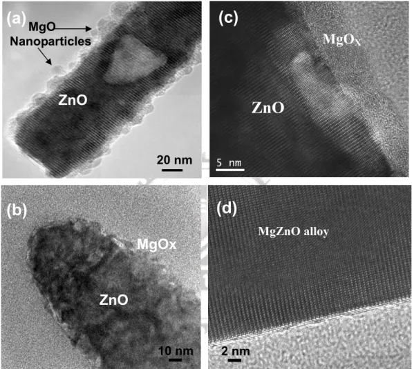
Chapter 4 Fabrication and characterization of MgO-doped ZnO
nanorod arrays... 34
4.1 Introduction...34
4.2 Surface morphologies after annealing treatments ...36
4.3 Annealing effect on photoluminescence...39
4.4 Summary...41
Chapter 5 Improvement of charge injection in nanostructured
ZnO/P3HT hybrid solar cells... 42
5.1 Introduction...42
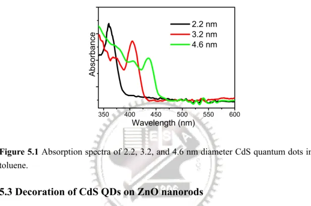
5.2 Optical properties of CdS QDs ...43
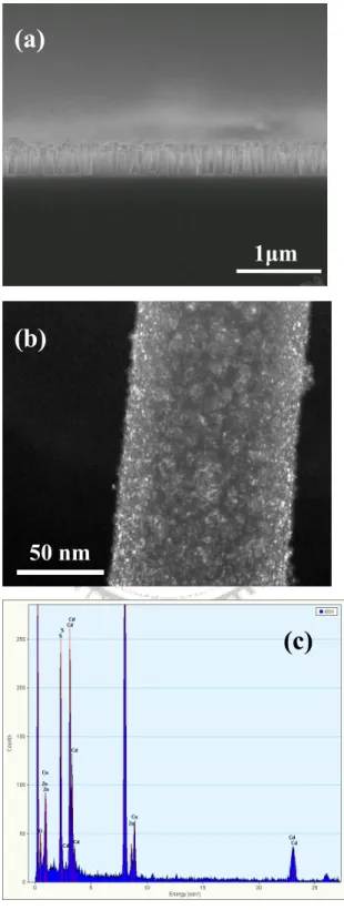
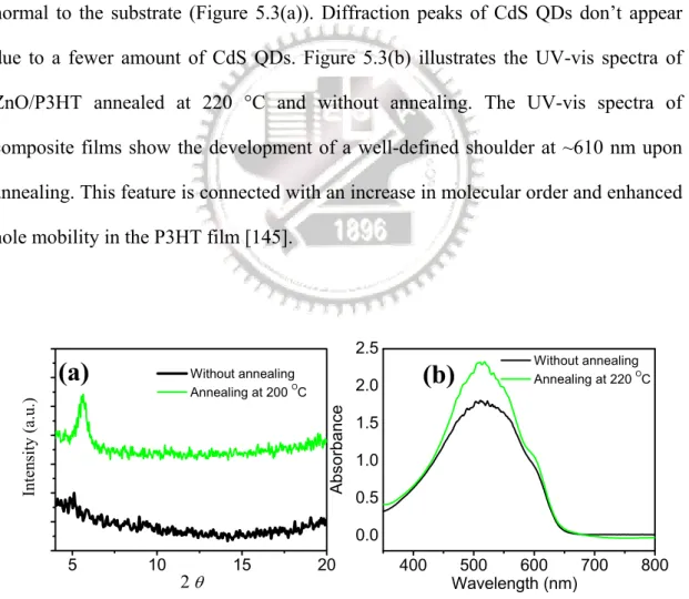
5.3 Decoration of CdS QDs on ZnO nanorods ...44
5.4 Annealing effect on P3HT ...46
5.5 Effect of CdS QD size ...47
5.6 Summary...51
Chapter 6 In-situ Growing CdS Single-Crystal Nanorods via
P3HT Polymer as a Soft Template... 52
6.1 Introduction...52
6.2 Effect of temperature...55
6.3 Effect of concentration ...56
6.4 Mechanism of CdS growth...59
6.5 Effect of solvent ratio...62
iv
6.7 Summary...67
Chapter 7 Annealing effect on Photovoltaic Performance for
Hybrid P3HT/Elongated CdS Nanocrystals Solar Cell ... 69
7.1 Introduction...69
7.2 Annealing effect on optical properties ...71
7.3 Annealing effect on thermal properties ...75
7.4 Annealing effect on photovoltaic performance ...77
7.5 Interaction between P3HT and CdS surface...78
7.6 Summary...84
Chapter 8 Improvement in Photovoltaic Performance for Hybrid
P3HT/elongated CdS nanocrystals solar cells with F-doped SnO
2Arrays ... 85
8.1 Introduction...85
8.2 Microstructure of FTO-coated ZnO nanorods...87
8.3 Effects of ZnO nanorod length and FTO thickness...91
8.4 CdS nanocrystal effect...97 8.5 Summary...100
Chapter 9 Conclusions... 101
References ... 104
Curriculum Vitae ... 133
Publication list... 134
v
Acknowledgments
First of all, I am greatly indebted to my advisor Prof. San-Yuan Chen for his kindness advices and useful discussions during my study period. He guided and encouraged me to use my potential to finish this thesis. Moreover, he taught me to how to research independently and deeply so I learned very much from him in academic research. In addition, I also have benefited much from his philosophy of life. I also sincerely thank Prof. Dean-Mo Liu for his fruitful discussions and constructive suggestions in thesis work. Moreover, Prof. Liu’s assistance in editing of the English led my papers to much less errors and fluency.
I would like to thank the colleagues in my lab. They always inspired and accompanied me through any difficulty that I have to be overcome. I cannot finish this thesis without them. Finally, I want to thank my family for their unconditional supports during my study period.
vi
摘要
太陽能電池的種類繁多,若以材料種類分類,可以分成:矽太陽能電池、無機 化合物太陽能電池、染料敏化太陽能電池、有機太陽能電池等。其中是以單晶 矽太陽能電池效率最高,但是其製作成本高,不符合經濟效益。而有機太陽能 電池的 在能源危機的世代,研究出適合的再生能源是當務之急。而再生能源中又以太 陽能電池受到大眾矚目。在太陽能電池領域中,矽太陽能電池一直是主要的發 展對象。雖然它的轉換效率相當的高,但是價格卻不便宜且需要耗費大量能量 來製造。因此發展大面積、低成本和低耗費量能的技術就顯得越來越重要。近 年來,一種由有機物和無機物所組成的太陽能電池開始被大量的研究,其優點 在於製作成本低,只需旋轉塗佈機便可以塗佈上作用層,再用加熱板加熱結晶, 屬於低溫製程。造價低加上厚度薄,若是用於塑膠基板上變成可橈式太陽能電 池,十分具有實用價值。因此在本論文主要在探討此一類型的太陽電池。 聚(3-己基噻吩)是目前最被廣泛被使用,因為其具有適合的能帶寬,高 吸收係數和電洞的傳導係數。在本論文中,聚(3-己基噻吩)/硫化鎘複合物的 合成,光學特性與太陽能電池元件的應用是主要的探討的部分。本論文首先利 用水溶液法合成氧化鋅奈米柱,接著包覆一層氧化鎂,再利用熱處理得到氧化 鎂摻雜的氧化鋅奈米柱。其光學和結構特性以 X 光繞射儀、穿透式電子顯微鏡、 光激發光譜來鑑定。接著合成不同直徑的硫化鎘量子點修飾在氧化鋅奈米柱上 再灌入聚(3-己基噻吩)製成太陽電池元件,發現因為量子侷限效應造成能階 位移而促使電子躍遷變容易所以元件的效率升提 4 倍相較於沒有量子點的元 件。然而雖然效率獲得提升,但是仍是太低,所以我們發展 in-situ 方法合成 聚(3-己基噻吩)/硫化鎘複合物,在此方法中我們利用聚(3-己基噻吩)的分vii 子鏈作為模板,藉由改變實驗條件合成出不同長寬比的單晶硫化鎘,接著探討 其太陽能轉換效率,發現轉換效率隨著長寬比而增加,當長寬比條件為 16 時可 得最佳效率達到 2.9%。另外,我們也開始經由熱處理來研究聚(3-己基噻吩) 和硫化鎘複之間的作用力和元件效率之間的關係。我們從聚(3-己基噻吩)/ 硫化鎘複合物的紫外光-可見光吸收光譜中發現藍位移且隨著長寬比增加而增 加。此外聚(3-己基噻吩)/硫化鎘複合物的熱性質也會受到長寬比影響。因此 可以推論硫化鎘的存在會減少聚(3-己基噻吩)的結晶度,而結晶度是可以經 由熱處理得到回復,因此轉換效率有隨著熱處理的溫度和時間增加明顯的提 升,然而過久的熱處理使得硫化鎘過度的聚集而造成轉換效率的衰退,而且此 現象隨到長寬比減少而更明顯。從核磁共振光譜得知聚(3-己基噻吩)分子鏈 和硫化鎘之間的作用力隨著長寬比而增強也因此因造成硫化鎘的聚集速率較 慢,而使得元件效率對熱的穩定性較佳。 最後我們嚐試利用三維的電極取代平面電極來提升轉換效率,因此我們利 用噴霧裂解法在氧化鋅奈米柱上製備具備低電阻率與高可見光穿透率的含氟氧 化錫透明導電薄膜。由結果得知,當奈米柱的長度增長時,轉換效率隨著提升, 但當長度長於 320 nm,高分子會有填充於奈米柱間隙不完全,造成轉換效率衰 退。當使用三維的電極時對具有較長長寬比的硫化鎘而言會有填充於奈米柱間 隙的問題,因此最佳的效率為 2.6%當長寬比條件等於 4。
viii
Abstract
Conventional solar cells were built from inorganic materials such as silicon. Although the efficiency of such conventional solar cells is high, very expensive materials and energy intensive processing techniques are required. The need to develop and deploy large-scale, cost-effective, renewable energy is becoming increasingly important. In recent years, a hybrid solar cell consisting of a combination of both organic and inorganic materials has achieved good power conversion efficiencies (PCE), which will become the focus in this thesis.
A series of P3HT/CdS composites have been synthesized to study the photovoltaic characteristics with ZnO nanorod arrays. First of all, we synthesize highly arrayed ZnO nanorod arrays via chemical process and attempt to fabricate MgO-doped ZnO nanorod arrays. The MgO-doped behavior and PL properties of single-crystal ZnO nanorods were investigated in terms of the annealing temperatures. Second, we evaluate an ordered organic-inorganic solar cell architecture based on CdS QD-decorated ZnO nanorod arrays encased in the hole-conducting polymer P3HT. A photovoltaic device based that has been decorated with CdS QDs yields power conversion efficiency over 4 times greater than that for a similar device without CdS QDs. The best device yields a short circuit current density of 1.38 mAcm-2 under Air Mass (A.M.) 1.5 illumination (100 mW cm-2), resulting in a power conversion efficiency of 0.21%. Third, we developed a novel method used to synthesize CdS single-crystal nanorods directly in the presence of conjugated polymer poly(3-hexylthiophene- 2,5-diyl) (P3HT), where the P3HT is acting as a molecular template for geometrical manipulation of CdS nanocrystals and in the meantime, as an
ix
efficient charge conductor in composite form. The mechanism of in-situ growth of high-aspect-ratio CdS nanorod is proposed based on spectroscopic analysis. A considerably improved PL quenching was detected for the nanorods and suggested a result of electronic coupling between the high-aspect-ratio CdS nanorods and the conducting polymer matrix. A photovoltaic device consisting of CdS nanorods with aspect ratio (AR) of ca. 16 and the conjugated polymer poly-3(hexylthiophene) was well assembled and showed a power conversion efficiency of as high as 2.9% under A.M. 1.5 Global solar conditions. We found that the interaction between polymer chains and the CdS nanocrystals increased with the aspect ratio and thus the optical and thermal properties of P3HT/CdS composites change with the aspect ratios. The interaction also affected changes in the morphology of the active layer upon thermal treatment. Therefore, the performances of P3HT/CdS nanocrystals devices dramatically depended on annealing condtions. Finally, hybrid CdS/P3HT photovoltaic devices using F-doped SnO2 (FTO)-coated ZnO nanorod arrays as electrodes were studied. The crystalline FTO made using the low-cost spray pyrolysis deposition (SPD) displayed a nominally complete and uniform coating over the entire outer surface of the ZnO nanorods. The incorporation of CdS into the P3HT much enhanced the Jsc of the devices with a nanorod FTO electrode. The PCE of the device with a ZnO nanorod length of 320 nm was increased from 0.37% for P3HT without CdS to 1.8% with CdS of aspect ratio=1 (spherical shape). With a further increase the AR of CdS nanocrystal to 4, the PCE was further increased up to 2.6%. Longer CdS nanocrystals conversely caused deterioration in PCE as result of the nanorod array morphology. These results indicate that, although increased nanorod length could improve the photocurrent and efficiency, other factors, such as P3HT infiltration, nanorod array morphology and CdS nanocrystal length are required for obtaining optimal performance of these devices.
1
Chapter 1
Introduction
Development of devices for conversion of solar energy into electricity has attracted a great attention in recent years due to strong interest in renewable energy and the problem of global climate changes. For many decades the solar cell industry has been dominated by inorganic solid-state devices, mainly based on silicon. Energy conversion efficiency of the best monocrystalline Si photovoltaic cells is nearly 25% [1, 2]. However, manufacturing of Si-based devices is very expensive due to strong requirement to the high purity of the crystalline semiconductor. Therefore, new ways of manufacturing solar cells that can scale up to large volumes and low cost are required. New materials or fabrication procedures that could reduce the cost of photovoltaic electricity substantially could help drive a rapid expansion in implementation of photovoltaic technology. Organic semiconductors such as conjugated polymers, small molecules and dyes, are particularly interesting for this purpose, largely because of the potential for processing such materials directly from solution, and so enabling low-cost manufacture of large-area thin semiconductor films. Because polymer cells have higher optical absorption coefficients than silicon, they are more efficient at absorbing light, which means that much thinner photovoltaic cells are required, such as poly(3-hexylthiophene- 2,5-diyl) (P3HT) and poly[2-methoxy-5-(3′,7′-dimethyloctyloxy)-1,4-phenylenevinylene] (MDMO-PPV). These conjugated molecules are electronically active because of their highly polarizable π-systems, which are hybridized orbitals based on the constituent p atomic orbitals. The π−π* optical transitions are strong (absorption coefficients greater than
2
~105 cm-1), typically fall in the visible, and can be tuned synthetically through
molecular design. Charge carrier mobilities as high as 10 cm2/V.s made them
competitive with amorphous silicon. Furthermore, organic semiconductors have several advantages: (1) low-cost synthesis and (2) easy manufacture of thin film devices by vacuum evaporation/sublimation or solution cast or printing technologies.
Polymer-based devices based on the use of bulk heterojunctions can provide a large contact area between the donor and acceptor species. Bulk heterojunctions are formed by spin casting the polymer and an electron acceptor from a common solvent. Common acceptors used in polymer bulk heterojunctions are fullerenes, polymers, and n-type inorganic nanoparticles. Up to now, most of the literature has focused on blends of P3HT and the n-type inorganic nanoparticles. In general, high-quality nanocrystals of II–VI semiconductors such as CdS and CdSe can be prepared by chemical synthesis. However, a high surface energy of the small-sized semiconductor crystals often leads to their aggregation or oxidation. Therefore, an organic layer is required for surrounding the nanoparticles to prevent such processes. One of the most popular method is pyrolysis of organometallic precursors (Cd(CH3)2, bis(trimethylsilyl)sulfide or bis(trimethylsilyl)selenium) in a mixture containing trioctylphosphine oxide (TOPO), tributhyl- or trioctylphosphine (TOP) and small amount of various phosphonic acids as a strong ligand for cadmium ions [3–6]. The organic ligand also ensures solubility of the nanocrystals in organic medium which is highly important for preparation of the nanoparticle–polymer blends. However, the organic ligand inhibits charge transfer between the polymer and the nanocrystals [7], resulting in a decreased power conversion efficiency. Therefore, an in-situ synthetic method was developed to directly grow CdS nanocrystals in a conducting polymer (P3HT) solution without surfactants or ligands and investigated the optical and photovoltaic properties of the P3HT/CdS composites in the thesis.
3
Another important polymer-based device technology stems from replacing
nanoparticle with a vertically aligned inorganic semiconductor nanostructure, e.g.
nanorod and nanotube arrays. The nanorods can help improve electron transport by
avoiding the particle-to-particle hopping that occurs in the n-type inorganic nanoparticles. Furthermore, nanorods provide direct conduction pathways for the electrons from the point of injection to the collection electrode. Most successful
organic/inorganic hybrid cells use transparent metal oxides, such as TiO2 or ZnO, as
the n-type semiconductor because of their high electron mobility, transparency, and
ease of processing. Groups at NREL [8] and Imperial College London [9] have
demonstrated EQE values of over 15% for P3HT–ZnO nanorod devices. Comparison with devices based on ZnO nanoparticles of similar diameter showed superior performance for the nanorod devices, apparently due in part to slower interfacial charge recombination in the nanorods than in the particles [9]. These polymer–ZnO nanorod devices have so far been limited by the relatively large rod diameters and correspondingly large pore volumes, which limit the efficiency of exciton dissociation, and by exciton harvesting, charge transport and Voc. Except creating the ideal nanostructure that enables maximum efficiency, we improved the charge transports between ZnO nanorod and P3HT by decorating CdS QDs to ZnO nanorods. Moreover, hybrid CdS/P3HT photovoltaic devices using F-doped SnO2 (FTO)-coated ZnO nanorod arrays as electrodes were studied in this thesis.
An improvement of the photovoltaic efficiency requires a clear understanding of structure–properties relationships and numerous challenges related to synthesis of the composite materials and fabrication procedure of the device still remain to be overcome. In this way, the thesis is organized as follows. In Chapter 2, we will give a general introduction to the materials,working principles and literature reviews of the polymer solar cells. The experiment steps and characterization techniques employed
4
in this work were outlined in Chapter 3, that is, X-ray diffraction (XRD), transmission electron microscope (TEM), ultraviolet-visible (UV-vis), photoluminescence emission (PL), Raman, DSC, and scanning electron microscopy (SEM) for structure and morphology characterization, and optical and thermal properties, and I-V curve measurement for efficiency. In Chapter 4, we synthesize highly arrayed MgO-coated ZnO nanorod arrays via wet-chemical process. The MgO-doped behavior and PL properties of single-crystal ZnO nanorods were investigated in terms of the annealing temperatures. In Chapter 5, we study the photovoltaic characteristics of P3HT/ZnO nanorod solar cells by decorating CdS quantum dots (QDs) with different sizes on ZnO nanorods. The modification with CdS QDs can serve not only as a photosensitizer but mainly as an energy funnel and/or an electronic mediator to significantly improve the electron injection efficiency from P3HT to ZnO nanorods. The power conversion efficiency of the photovoltaic device based on that decorated with CdS QDs will be studied and compared with that for a similar device without CdS QDs.
In Chapter 6, we report a novel in-situ method to synthesize CdS single-crystal nanorods directly in the presence of conjugated polymer P3HT, where the P3HT is acting as a molecular template for geometrical manipulation of CdS nanocrystals and in the meantime, as an efficient charge conductor in composite form. Such a templating process allows the CdS nanorods with various aspect ratios to be easily manufactured via a controlled solvency of a co-solvent mixture, under which the conformational variation of the P3HT chain can be manipulated.
In Chapter 7, we focus on interaction between the P3HT and the CdS surface. 1H NMR analysis indicates physical attachment between the CdS nanocrystals and the thiophene ring of P3HT; the interaction strength between the P3HT and CdS surface increases with the AR. The UV-vis spectra of the P3HT/CdS composite films show a
5
blue shift with an increasing AR of the CdS nanocrystals because CdS nanocrystals destruct the ordered structure of polymer chains as evidenced by the decrease in the melting point of P3HT main chain crystals. Atomic force microscope measurements on P3HT/CdS film demonstrate the aggregation of CdS nanocrystal in the P3HTmatrix is more apparent for the CdS nanocrystals of AR=4 than that of AR=16. It is concluded that upon annealing, a stronger interaction between P3HT and CdS for a larger AR (16) tend to reduce the CdS aggregation, which is favorable for the network structure and formation of percolation paths to increase the transport properties of the P3HT/CdS solar cells. Therefore, the PCE of the in-situ-growth P3HT/CdS with AR=16 composite shows a higher Photovoltaic performance.
In Chapter 8, we reported hybrid CdS/P3HT photovoltaic devices using F-doped SnO2 (FTO)-coated ZnO nanorod arrays as electrodes using the low-cost spray pyrolysis deposition (SPD). The photovoltaic performance of CdS/P3HT photovoltaic devices was studied as a function of FTO-coated ZnO nanorod length and thickness of the FTO layer. However, although increased nanorod length could improve the photocurrent and efficiency, other factors, such as P3HT infiltration, nanorod array morphology and CdS nanocrystal length are required for obtaining optimal performance of these devices. Finally, conclusion and future researches will be summarized in Chapter 9.
6
Chapter 2
Theory and Literature Review
2.1 Electrical Characteristics of a Solar Cell
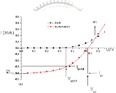
In Figure 2.1, the current-voltage characteristics are shown for a solar cell in the dark and under illumination. In the dark, there is almost no current flowing, until the contacts start to inject heavily at forward bias for voltages larger than the open circuit voltage. Under illumination, the current flows in the opposite direction than the injected currents. At (a) the maximum generated photocurrent flows under short-circuit conditions; at (b) the photogenerated current is balanced to zero (flat band condition). Between (a) and (b), in the fourth quadrant, the device generates power (i.e., current × voltage). At a certain point, denoted as maximum power point (MPP), the product between current and voltage and hence the power output is largest. The photovoltaic power conversion efficiency (ηe) of a solar cell is determined by:
e η = in SC OC P FF I V × × (2.1) FF = OC SC mpp mpp V I V V × × (2.2) where VOC is the open circuit voltage, Isc is the short-circuit current, FF is the fill
factor and Pin is the incident light power density, which is standardized at 1000 W/m2 for solar cell testing with a spectral intensity distribution matching that of the sun on the earth’s surface at an incident angle of 48.2o, which is called the AM 1.5 spectrum [10]. Impp and Vmpp are the current and voltage at the maximum power point in the fourth quadrant of the current–voltage characteristics.
7 I= PH SH S S I R IR U IR U nkT e I0⋅{exp( ( − ))−1}+ − − (2.3)
where I0 is the dark current, e the elementary charge, n the diode ideality factor, U the applied voltage, RS the series, RSH the shunt resistance, and IPH is the photocurrent. The corresponding equivalent circuit is depicted in Figure 2.2. For a high FF, two things are required: (1) that the shunt resistance is very large to prevent leakage currents and (2) that the series resistance is very low to get a sharp rise in the forward current. The series resistance simply adds up from all series resistance contributions in the device, that is, from bulk transport, from interface transfer and from transport through the contacts.
Figure 2.1 Current–voltage (I–V) curves of an organic solar cell (dark, dashed; illuminated, red, full line).
Figure 2.2 Equivalent circuit for a solar cell.
RS
RSH
IPH
8
2.2 Hybrid Conjugated Polymer-Semiconductor Solar Cells
A key development for polymer-based photovoltaic (PV) cells came from Tang [11] when he demonstrated the concept of bringing two semiconductors into contact to increase the power conversion efficiency (PCE). This interface is known as a heterojunction. The first dispersed polymer heterojunction PV cell was demonstrated by Yu et al. [12] in 1994. Nanoparticle–polymer cells generally have a photoactive layer consisting of interconnected semiconducting nanoparticles in a solid semiconducting polymer phase [13]. Crystalline inorganic nanoparticles have several attributes as electron acceptors, including relatively high electron mobility, high electron affinities, and good physical and chemical stability. The nanoparticles have at least one dimension within the range of 1 nm to ca. 100 nm that they are colloids. It combines the unique properties of inorganic semiconductors with the film-forming properties of the conjugated polymers [14]. Organic materials usually are inexpensive, easily processable, and their functionality can be tailored by molecular design and chemical synthesis. On the other hand, inorganic semiconductors can also be manufactured as processable nanoparticulate colloids and solution-processible nanocrystalline semiconductors that can be prepared in different morphologies offer the potential for a large area interface when combined with a solution-processed organic component.
Excitons created upon photoexcitation are separated into free charge carriers at interfaces between a conjugated polymer and inorganic semiconductors. Electrons will then be accepted by the material with the higher electron affinity (electron acceptor, inorganic semiconductors), and the hole by the material with the lower ionization potential, which also acts as the electron donor. The solubility of the n-type and p-type components is an important parameter of the construction of hybrid solar
9
cells processed from solutions. By varying the size of the nanoparticles, their band gap can be tuned and their absorption/emission spectra can be tailored [15].
2.2.1 Working Principles of Polymer-Semiconductor Solar Cells
The energy levels for a general polymer cell are shown in Figure 2.3. The photoactive layer contains a light harvesting material which acts as a photon absorber. Photons with energy greater than the band gap (Eg) are absorbed by the photoactive layer to create a neutral exciton by promotion of an electron from the highest occupied molecular orbital (HOMO) to the lowest unoccupied molecular orbital (LUMO) of the light harvesting polymer. An exciton can be considered as a bound electron-hole pair. The average length over which the exciton can diffuse within the polymer before recombination of the hole and electron occurs is the exciton diffusion length, Lex (⋍10 nm for P3HT). Exciton dissociation can take place at a suitable junction provided that recombination does not compete. (Recombination, which is the process whereby an electron and hole combine, results in annihilation of the charge carrier.) After dissociation the charges migrate to their respective electrodes as a result of an internal electric field generated by the difference in their Fermi levels.
Figure 2.3 Energy levels and the harvesting of energy from a photon for an acceptor/donor interface within a photoactive layer of a PV cell.
Donor Acceptor HOMO (or VB)
LOMO (or CB) h+ e -e -hv Photocathode Photoanode
10
As mention above, each step has different efficiency and their product determines the external quantum efficiency (EQE) [16]:
EQE=ηAηdiffηsepηtrηcc (2.4) In Eq. (2.4) η is the photon absorption yield (the number of generated excitons/the A number of incident photons). This is determined by the optical absorption coefficient of the photoactive layer and its thickness.
The parameter ηdiff is the charge carriers diffusion yield (the number of diffusing excitons to the D–A interface/the number of generated excitons). If the average diffusion length that the exciton must travel to reach a heterojunction is relatively large compared to Lex then recombination of the charge carriers is favored andηdiff<1.
sep
η is the charge carries separation yield (the number of dissociated
excitons/the number of excitons at the interface) which is the probability that the hole and electron will be separated by the internal electric field at a heterojunction. In most polymer semiconductors excitons have a binding energy of a fraction of an eV (below) and it is necessary to incorporate materials with a suitable offset in the energy levels within the photoactive layer to dissociate these excited states. In nanoparticle–polymer PV cells the nanoparticles have a relatively low electron affinity and accept electrons from the polymer under illumination. The electrons are accepted by the LUMO (in the case of organic nanoparticles) or the conduction band (in the case of inorganic nanoparticles) (Figure 2.3). The polymer acts as an electron donor. This process results in exciton dissociation. The energy required to separate the exciton [17] is ca. 0.4 eV in a polymer semiconductor. In a well designed nanoparticle–polymer cell the energy required to separate the exciton is provided by
11
the energy difference (offset) between the LUMOs of the donor and acceptor Figure 2.3).
tr
η is the charge transport yield in the donor and acceptor materials (the number of the free charge carriers transported to the collecting electrode/the number of the charge carriers dissociated at D–A interface). Charge transport involves hopping processes and is affected by traps in the composite film. Traps originate from structural defects or impurity species. They provide localized energy minima of variable depth for charge transport which reduce charge mobility.
cc
η is the charge collection yield (the number of the charge carriers in the external circuit/the number of the charge carriers transported to the electrode). The collection of charge at the electrodes is crucial to overall efficiency. This parameter represents the ability of the charges to be transferred from the photoactive layer to the electrodes. It is a function of the energy levels of the components (Figure 2.3) and the interfacial contacts between the photoactive layer and the electrodes. High ηcc values can occur when (a) the Fermi level of the photoanode is greater than the energy level of the donor's HOMO and (b) the energy level of the acceptor's LUMO is greater than the Fermi level of the photocathode (Figure 2.3).
In photovoltaic p–n junction cells the driving force for the charge transport is a built-in potential Vbi [18]. According to the simplified model, in metal/insulator/metal devices it corresponds to the difference between the work functions of the collecting electrodes and may be estimated by measuring the open circuit voltage, VOC, at high illumination intensity and zero dark current. It turns out, however, that the barrier height only weakly depends on the metal used, because of Fermi level pinning to the semiconductor due to the presence of interface surface states and/or defects [19]. The Fermi level pinning describes a situation where the work function of the metal electrode is pinned to the work function of the semiconductor. Similar approach has
12
been applied to explain an origin of the open circuit potential of organic photovoltaic cells, based on conjugated polymer and fullerene derivatives. Brabec et al. [20–22] have found that the value of VOC in these cells is directly related to the energy
difference of HOMO level of the donor and the LUMO level of the acceptor components. This electrode-insensitive voltage behavior was ascribed to the Fermi level pinning of the negative metal electrode to the reduction potential of fullerene via charged interfacial states. Thus, the VOC value in plastic solar cells is mainly related to
the electronic structure of acceptor and may be tuned by molecular engineering. In addition, the value of VOC is also influenced by an interfacial factor associated with
different morphology of composite films [23]. Moreover, the value of VOC in
semiconductor–polymer hybrid cell may be influenced by the size of nanorod diameter, according to tendency of the increase of the bandgap energy with decrease of the nanostructure size.
2.2.2 Competitive processes in the hybrid systems
A flux of photo-generated charge carriers, responsible for the value of photocurrent may be diminished by several processes: (1) Recombination in the bulk, when the travel path of the excitons is longer than their diffusion length. Since the exciton diffusion lengths in various conjugated polymers ranges from 5 to 20 nm [24], the electron–hole recombination may be diminished by preparation of the bulk heterojunction solar cell with nanostructures well distributed in the polymer phase. (2) Back-transfer recombination, when the hole from the conducting polymer recombines at the interface with the electron from semiconductor [25]. This type of recombination is strongly influenced by unbalanced hole and electrons mobilities in corresponding materials. Since the electron mobility exceeds hole mobility by two orders of magnitude, the improvement of the hole transport mobility in the polymer should
13
significantly improve the PV cell performance [26]. The recombination is also strongly enhanced if the charge transport towards the electrodes is hindered by the domain boundaries between the electron donating and accepting materials [27], leading to a strongly morphology-dependent quantum efficiency of hybrid PV cell [28, 29].
2.3 Materials used in the photoactive layer
2.3.1 Conducting Polymers used in the photoactive layer
Conjugated polymers in the polymer–semiconductor hybrid systems can play both the role of photoactive materials as well as acceptor of holes. The electron transfer from conjugated polymers to the semiconductor phase may be detected by measurement of quenching of photoluminescence from conducting polymer after addition of semiconductor nanocrystals [30–32] or by photoinduced absorption experiments [33].
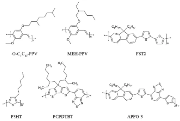
The chemical structures for polymers usually used in nanoparticle– polymer PV cells are shown in Figure 2.4. All of them are hydrophobic and have extensive conjugation. Table 1 gives parameters that are important from the viewpoint of PV cell performance. With the exception of PTAA, the polymers are used for photogeneration as well as charge transport. (PTAA has a relatively large Eg value and is less suited for photogeneration.) P3HT is the most widely used semiconducting polymer for nanoparticle–polymer PVs due to very high value of the hole mobility and good processability.
14
Figure 2.4 Chemical structures of selected polymers commonly used in hybrid solar cells.
Table 1 Selected parameters for conducting polymers used in hybrid polymer–semiconductor PV cells.
Polymer ELUMO (ev) EHUMO (ev) Eg (ev) Hole mobility (cm2V-1s-1) Ref
P3HT (NR) -2.55 -4.65 2.1 10-5 to 10-4 151 P3HT (RR) -3.0 -4.90 1.9 0.05-0.1 155 MEH-PPV -2.9 -5.3 2.4 10-4 to 10-3 156 OC1C10-PPV -3.0 -5.26 2.86 10-6 158 F8T2 -3.1 -5.5 2.4 0.01-0.02 143 APFO-3 -3.53 -5.84 2.31 3.1x10⁻⁵ 148
The characterisation of conjugated polymers used in nanoparticle–polymer PVs usually involves electrical property, structure and chain length measurements. The electrical properties are defined by the energy levels (EHOMO, ELUMO and Eg) as well as the mobility. The position of the HOMO levels is important for the PCE of nanoparticle-polymer PVs as well as its stability to oxygen. The ionisation potential of a conjugated polymer directly affects VOC as well as the stability to air. Previous
studies have shown that the ionisation potential should not be lower than [34] ca. 5.2 eV otherwise the polymers are susceptible to oxidation by O2. Generally the ionisation potential of a polymer can be tailored by adding electron withdrawing or donating substituents to the main chain. An important factor taken into account in choosing the most preferable conducting polymer as the composite material for PV cell is the
15
position of the HOMO and LUMO energy levels with respect to the energy of conducting and valence bands of semiconductor. Because lowering of the Eg allows moving the limit for absorption of photons, a significant increase of the number of excitons created under illumination may be achieved.
The hole and electron mobilities of polymers also affect PCE because high mobilities are essential within polymer-based PVs in order to minimize recombination losses. Mobilities of ca. 10−3 cm2 V-1 s−1 are needed to prevent photocurrent losses for PV cells with thickness of several hundred nanometers. The mobility can be determined by applying a saturation regime equation to the measured I vs. V data [35]. The conducting polymers in the neutral state the typical values range from 10−1 to 10−7 cm2 V-1 s−1 for holes [36, 37] and from 10−4 to 10−9 cm2 V-1 s−1 for electrons [38, 39]. The charge transport in the conducting polymer may be enhanced by the increase of degree of polymer regioregularity (RR) by means of regioselective synthesis of the polymer [40–42]. This relationship has been widely studied for poly(3-alkylthiophenes) (PATs). For example, the hole mobility in the neutral regioregular PATs, with over 95% of head-to-tail couplings, ranges from 10−3 to 10−1 cm2 V-1 s−1 [43–45] compared with 10−5 to 10−4 cm2 V-1 s−1 in regiorandom analogues [46, 47]. This is because the HT coupling of the monomer units in RR polymer essentially favors a rod-like form, in contrast to more twisted chains in regiorandom polymer. In several reports [37, 48, 49] the high mobility of the charge carriers in RR polymers has been ascribed to the interchain π-π stacking, which results in delocalization of the charge carriers over the several neighboring chains. In effect, the charge carriers may easily hope between the chains giving rise to the higher mobility. According to Sirringhaus et al. [48] the interchain π-π stacking leads to the self-organization in P3HT film in a lamella structure with twodimensional conjugated sheets. In addition the mobility generally increases with molar mass because fewer
16
hopping events are required for films composed of longer chains.
The structure investigations involve chain packing and morphology. A combination of out-of-plane and in-plane grazing incidence XRD is well suited to study P3HT matrix structure [35]. The morphology of the films is usually studied by AFM and SEM. These studies have shown that within P3HT films the chains can form well-defined nanorods [35] when the molar mass was less than 4000 g mol−1. A less ordered structure occurred at higher molar masses.
2.3.2 Inorganic Nanoparticles used in the photoactive layer
Conjugated polymer-semiconductor solar cells have been demonstrated in various semiconducting polymer blends containing CdSe [49-51], CdS [52], CuInS2 [14], or PbS [53] nanocrystals. This strategy is promising for several reasons [54]: (1) Inorganic semiconductor materials can have high absorption coefficients and photoconductivity as many organic semiconductor materials. (2) The n- or p-type doping level of the nanocrystalline materials can easily be varied by synthetic routes so that charge transfer in composites of n- or p-type organic semiconducting materials with corresponding inorganic counterparts can be studied. (3) If the inorganic nanoparticles become smaller than the size of the exciton in the bulk semiconductor (typically about 10 nm), their electronic structure changes. The electronic and optical properties of such small particles depend not only on the material, of which they are composed but also on their size [15, 49, 55-57]. Band-gap tuning in inorganic nanoparticles with different nanoparticle sizes can be used for realization of device architectures, such as tandem solar cells in which the different bandgaps can be obtained by modifying only one chemical compound [58, 59]. A substantial interfacial area for charge separation is provided by nanocrystals, which have high surface area to volume ratios [51].
17
High surface tension of very small inorganic nanocrystals makes them unstable, and thus they have a tendency to grow to larger particles by a process called “Ostwald ripening” [60]. Therefore, nanoparticles are synthesized commonly shielded by an organic ligand. For example, nanocrystals of II–VI semiconductors such as CdS and CdSe can be prepared by chemical synthesis. One of the most popular method is pyrolysis of organometallic precursors (Cd(CH3)2, bis(trimethylsilyl)sulfide or bis(trimethylsilyl)selenium) in a mixture containing trioctylphosphine oxide (TOPO), tributhyl- or trioctylphosphine (TOP) and small amount of various phosphonic acids as a strong ligand for cadmium ions [3–5]. A high surface energy of the small-sized semiconductor crystals leads to their aggregation or oxidation. An organic layer surrounding the nanoparticle can prevent such processes and also ensures solubility of the nanocrystals in organic medium which is highly important for preparation of the nanoparticle–polymer blends. However, this organic ligand, on the other hand, is a barrier for transport of charges from nanoparticle to nanoparticle. Therefore, in the hybrid solar cells, such ligands have to be removed to ensure intimate electrical contact between the nanoparticles [56, 61].
The growth conditions and the shape of nanocrystals, from dots to 1D rods of different length (Figure 2.5 (a)–(d)) and to branched structures, may be optimized by manipulating the composition of the reaction solution, concentration of reagents, temperature, as well as the injection method [62–64]. Manna et al. [65] have demonstrated that the formation of CdSe nanocrystals with rod, arrow, snowflake and tetrapod shapes may be controlled by variation of the ratio of trioctylphosphine oxide and hexylphosphonic acid used for synthesis. Recently, Manna and co-workers [66] have reported a more general approach for synthesizing of tetrapod-shaped nanocrystals made of various combinations of II–VI semiconductors. This method, based on a seeded-growth process, allows varying independently the compositions of
18
the core and the arms of tetrapods. The nanoparticle geometry and aspect ratio (AR) have a strong influence on PCE. Nanoparticles with moderate aspect ratios generally increase the PCE for inorganic nanoparticle–polymer PV cells.
Figure 2.5 TEM images of (a) 7 nm×7 nm, (b) 8 nm×13 nm, (c) 3 nm×60 nm, (d) 7 nm×60 nm CdSe nanocrystals and (e) TEM image of a film prepared from 40 wt% 3 nm×60 nm CdSe nanorods in P3HT, spin cast from the mixture of 10 vol% pyridine in chloroform. [69].
In general, the synthesis of CdS nanorods may be also performed by thermal decomposition of single-molecule precursor, Cd(S2CNEt2)2, in the presence of hexadecylamine as surfactant [67]. The use of single precursor has an advantage of avoiding the toxic and explosive cadmium compounds and eliminating the undesired effects of additional ions during the synthesis. The shape and size of nanostructures may be controlled by temperature and precursor concentration. Thermal decomposition method has been also used for synthesis of TOPO-capped CuInSe2 sharp-edged nanoparticles with dimensions of approximately 15nm by 20nm [68, 69]. There are also several other highly perspective methods of obtaining of semiconductor nanorods and/or more complex structures (tetrapods, arrows), like soft template methods (such as liquid crystal [70] and micellar [71–73]), structure-directing
19
coordinate solvent methods (such as solvothermal route [74–76]) and vapor–liquid–solid (VLS) [77] and solution–liquid–solid [78] methods.
The ligand used during synthesis of nanocrystals protects before aggregation of particles but on the other hand, it forms a barrier of several Angstrom thickness around the nanocrystals. Then, after blending with the conjugated polymer, the barrier of ligand may decrease the conversion efficiency of hybrid material by impeding the transport of the electrons between the adjacent nanocrystals [52] and between conducting polymer and nanocrystals. It has been found however, that the surface ligand can be changed without altering the intrinsic electronic properties of nanocrystal. Huynh et al. [64] have shown that the TOPO can be replaced by a weak-binding ligand, as pyridine, allowing also for a uniform distribution of CdSe nanocrystals in poly(3-hexylthiophene) film obtained by spin-coating from pyridine–chloroform solution (containing from 4 to 12 vol% of pyridine, see Figure 2.5 (e)). However, too much pyridine is not recommended to avoid precipitation of P3HT, which is soluble in chloroform but insoluble in pyridine. Moreover, pyridine may also act as non-radiative recombination site leading to decrease of the external quantum efficiency of the PV device and therefore, it should be removed from the hybrid layer by heating.
2.4 Methods of preparation of polymer-semiconductor solar cells
Hybrid polymer–inorganic structures can be prepared in different ways: (1) a planar bilayer structure where an organic layer is deposited on top of an inorganic semiconductor layer, (2) nanostructured porous structures where a connected semiconductor layer is filled with a conjugated polymer, and (3) blends of nanocrystals with polymer where semiconductor nanoparticles and polymer are deposited from the same solution. The inorganic semiconductors studied for hybrid
20
devices have included II–VI and I–III–VI compound semiconductors, which, critically, also offer optical absorption in the red part of the spectrum [52], and metal oxide semiconductors.
2.4.1 Bilayer heterojunctions
The easiest way is to prepare a bilayer heterojunction. In a bilayer heterojunction device, p-type and n-type semiconductors are sequentially stacked on top of each other, as shown in Figure 2.6. The semiconductor may be deposited chemically [79, 80] or electrochemically [81] on the transparent ITO and covered by drop-casting or spin-coating with the conducting polymer. However, due to relatively small area of interfacial surface, this type of hybrid systems is not perspective. The efficiency of bilayer solar cells is limited by the charge generation 5-15 nm (exciton diffuse length) around the donor-acceptor interface. Since a typical absorption depth in conducting polymer is about 100 nm, most of absorbed photons are lost due to recombination of the excitons created at the distance above the diffusion length.
Figure 2.6 Bilayer configuration in organic solar cells.
ITO glass PEDOT-PSS Aluminum Light N-type P-type
21
2.4.2 Bulk heterojunctions
The limitation in a bilayer heterojunction may be overcome by preparation a bulk heterojunction cell. Bulk heterojunction is a blend of the donor and acceptor components in a bulk volume (Figure 2.7). The both components are usually prepared separately, blended in organic solvent and then grafted on the substrate. The blend exhibits a donor-acceptor phase separation in a 5-15 nm length scale. In such a nanoscale interpenetrating network, each interface is within a distance less than the exciton diffusion length from the absorbing site. The bulk heterojunction concept has heavily increased (orders of magnitude) the interfacial area between the donor and acceptor phases and resulted in improved efficiency solar cells [82]. Meanwhile, separated charges require percolated pathways for the hole and electron transporting phases to the contacts. In other words, the donor and acceptor phases have to form a nanoscale, bicontinuous, and interpenetrating network [83]. Therefore, the bulk heterojunction devices are much more sensitive to the nanoscale morphology in the blend. Optimal morphology is achieved by a careful balance between the nanoparticle aggregation needed for good charge transport and phase separation needed for efficient exciton dissociation. Wang et al. [84] have postulated that the capped pyridine molecules at the CdS surface facilitate dissolution of CdS nanocrystals in the pyridine solvent. Moreover, pyridine acts as a surfactant which improves compatibility of CdS nanocrystals with the polymer chains (MEH-PPV) both in the solution and in the solid film. Homogeneous dispersion of nanoparticles in the polymer blends leads to the larger area of donor–acceptor interface which could improve the charge separation efficiency.
22
Figure 2.7 Bulk heterojunction configuration in organic solar cells.
The performance of photovoltaic devices may be also controlled by changing the size, shape and concentration of nanocrystals. The influence of semiconductor nanoparticle content on the efficiency of PV hybrid cell has been studied by Greenham at al. [52]. It has been shown that at low concentrations of spherical 5 nm CdSe nanoparticles in MEH-PPV only part of electrons have a continuous pathway to the external circuit. At higher concentrations (65 wt%) the nanocrystals begin to form a connected network and both components provide continuous ways for the charge carriers to the electrodes. The highest EQE (12%) was obtained at 90 wt% of CdSe. However, even at the optimum concentration, the EQE is still low due to trapping of the electrons at “dead ends” in the nanocrystal network. Therefore, the much effort was focused on preparation of the hybrid cells containing nanorods or branched semiconductor structures.
It has demonstrated that one-dimensional nanorods [50, 64] or branched semiconductors [85–89] are used to create the percolation networks in the polymer/semiconductor blend improving the charge transport through the semiconductor phase to the electrode. Huynh at al. [50, 64] have demonstrated that change of the aspect ratio of CdSe nanocrystals from 1 to 10 results in the increase of
ITO glass PEDOT-PSS Aluminum
Light
23
the external quantum efficiency at the wavelength of 500 nm from about 18% to 54%, respectively (Figure 2.8). By contrast, the cells containing hyperbranched CdSe approached maximum PCE values at lower nanoparticle concentration values than the other nanoparticle geometries [85]. Gur et al. [85] argued this was because of more efficient formation of charge transfer pathways. Furthermore, the cells based on hyperbranched particles revealed near-linear rise of JSC and power conversion
efficiency with increased loading of CdSe, also at a low content of nanostructures. This suggests that single incorporated hyperbranched particle can contribute independently to the output of the cell [85].
In another paper Gur et al. have shown that a unique tetragonal structure of CdTe nanocrystals gives rise to a natural ordering in the deposited films [90, 91]. Namely, three arms of each tetrapod contact the substrate at its base, while the fourth arm points up, perpendicular to the substrate. This ordering remains in the composite films created by spin-coating of the polymer–nanocrystal mixture. However, the efficiency of the device based on CdTe tetrapods and P3HT spin cast from chloroform solution are still low (less than 1%), suggesting the need of further improvement by optimization of device composition and morphology [90].
Figure 2.8 Influence of the increasing length (7, 30 and 60 nm) of 7-nm diameter CdSe nanorods on the external quantum efficiency of CdSe (90 wt%)/P3HT 200-nm thick solar cell. [50]
24
One of the major difficulties in preparation of the bulk heterojunction cell is the phase segregation of organic and inorganic phases. The key parameters are processing conditions as the type of the solvents used for preparation of the polymer/semiconductor mixture and temperature which control the rate of drying of the hybrid system. The influence of the rate of solvent evaporation on the formation of the π-stacked aggregates and in consequence, on the charge carrier mobility, has been also confirmed [92–94]. Yang et al. [94] have shown that drop-casting of P3HT reinforces the lamellar π-π stacking perpendicular to the substrate, depending on the type of solvent. The charge mobility in the film decreases in the order CHCl3 > THF > toluene > CH2Cl2. The significantly lower charge mobility in the films deposited from toluene and dichloromethane was attributed to the formation of distinct grain boundaries and the short nanorod-like structures. In contrast, the polymer chains cast from CHCl3 form highly interconnected nanofibrillar networks without grain boundaries providing fast charge transport through the film.
Solvent evaporation causes a transition from a one phase to a two phase region. Extensive nanoparticle aggregation and phase separation of the polymer phase is favored as nanoparticle and polymer volume fraction increase. In well-controlled solvent evaporation processes this gives a bicontinuous solid dispersion. It is in this way that non-equilibrium morphologies can be frozen (kinetically trapped) into the photoactive layers of nanoparticle–polymer PV cells.
Phase segregation during casting may lead to formation of “dead ends” and isolated domains trapping the charge carriers. The polymer wetting and charge transfer dynamics may be improved by means of interface modifiers. One option is to use a surfactant containing the head group of a high affinity to semiconductor and the end group providing solubility in the chosen solvent. Milliron et al. [95] have
25
demonstrated that pentathiophene phosphonic acid (T5-PA), served as a complexing agent with respect to the CdSe nanocrystals, could be used as a third component in nanocrystal–polymer devices mediating the charge transport between these two materials.
Alternative approach applied by Liu et al. [96] consisted in functionalization of the polymer chain ends with amine groups, which are strongly adsorbed onto CdSe nanoparticles. The endamino groups attached to the P3HT replace the pyridine surfactant on the surface of nanorods and thereby enhance the miscibility of the polymer with the nanocrystals and improve the power conversion efficiency of hybrid device. The ligand-exchange method has been also applied to graft the carbodithioate-containing oligo- and polythiophenes on the CdSe surface [97].
Another strategy, which utilizes direct attachment of P3HT onto the CdSe nanorod surface, has been applied by Zhang et al. [98] by coupling of vinylterminated P3HT to arylbromide-functionalized CdSe. The recent advances in preparation the organic–inorganic nanohybrids through tailoring of semiconductor nanocrystals with conjugated polymers have been discussed by Lin in the review paper [99].
An efficient way of impeding the phase segregation is also to induce strong interaction between organic–inorganic components through molecular recognition phenomena. This concept has been successfully used by De Girolamo et al. [100] in preparation of the composites of diamino-pyrimidine functionalized P3HT with thymine-capped CdSe nanocrystals. This molecular processing method has been also exploited for the alternating deposition of thymine-capped nanocrystals and functionalized polymer monolayers by layer-by-layer assembly [101].
Thermal treatment of the polymer in the vicinity of its melting temperature (Tm) was proven to be an effective method to increase the hole transport velocity due to enhanced chain ordering (π-stacking) [102,103] and self-organization of the polymer
26
[64]. According to Wang et al. [84], improvement of the device performance after annealing is mainly attributed to reorganization of the inorganic nanocrystal/polymer interface, leading to the increase of exciton dissociation efficiency and reduction of the recombination loses. It may be also a result of reduced interface defects [104] and improved phase-structured morphology [105]. Dittmer et al. [106] have postulated that annealing of hybrid system promotes the equilibrium morphology of a spin-coated film, improves crystallinity within the phase-separated networks and thereby facilitates the charge transport to the electrodes. Thermally induced crystallization enhances also of the efficiency of the charge transport across the interface between the bulk of material and the collecting electrode (ηtr). Most of the reports in the literature on the influence of annealing on the efficiency of hybrid cells concern the polymer/PCBM systems but the mechanism of performance enhancement for the polymer/inorganic semiconductor hybrid systems is less clear.
2.4.3 Porous and Vertically ordered semiconductor–polymer systems
There are also several attempts to prepare the PV cells on the base of nanostructured large-band gap semiconductors. This approach was used to combine TiO2 with conjugated polymer [107-109] because TiO2 can be easily obtained in the form of mesoporous material [110] providing the continuous network for electron transport. In PV cell developed by Coakley and McGehee [107] the conducting polymer (P3HT), acting as solid-state sensitizer, was infiltrated into 100nm thick mesoporous TiO2 film. The external quantum efficiency was about 10%, whereas the power conversion efficiency under monochromatic illumination (at 514 nm) was1.5%. A shortcoming of this type of the cell is poor polymer penetration in the porous structure, small interfacial area, slow transport of the holes generated in the polymer in a distance longer than 10–20 nm from the top of the film and back recombination with the
27
electrons from TiO2.
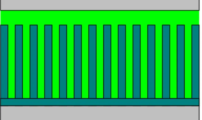
The photovoltaic performance of the devices may be improved by structuring one of the components into vertically ordered rods or pores with a diameter less than the exciton diffusion length, as displayed in Figure 2.9. The two phases have to be interdigitated in percolated highways to ensure high mobility charge carrier transport with reduced recombination. Last but not least, a pure donor phase at the hole collecting electrode and a pure acceptor phase at the electron collecting electrodes have to be placed. This minimizes the losses by recombination of the wrong sign of charges at the wrong electrode, as well as acting as diffusion barriers for the wrong sign charge carriers at the respective electrodes. Ordered heterojunctions are generally made by infiltrating polymers into vertically aligned oxides, such as nanorods and nanotubes. Nanostructured TiO2 or ZnO is an attractive approach to develop extremely efficient organic photovoltaics. They are abundant, nontoxic, and has been well-studied by the dye-sensitized solar cell community.
An alternative approach for vertical alignment is single-crystal nanorod arrays of other semiconductors (CdS, CdSe). They have been obtained by electrochemical synthesis using a hard template of anodic aluminum oxide (AAO) [111–116]. Kang and Kim [153] have applied such a matrix to construct the heterojunction solar cells with vertically aligned CdS nanorods and pores filled in with MEH-PPV.
The nanostructure in Figure 2.9 is considered ideal because it has small, straight pores and is thick enough to absorb most of the sunlight. The pore radius should be slightly less than the exciton diffusion length to enable maximum exciton harvesting. The thickness of the nanostructure should be 300–500 nm so that the infiltrated polymer can absorb most of the incident light. The pores (or channels) should be straight to provide the most direct path to the anode and cathode.
28
Figure 2.9 Scheme of polymer–inorganic semiconductor hybrid system with vertically aligned semiconductor nanostructures.
Currently, the most efficient ordered nanostructured oxide/polymer device is significantly worse than bulk heterojunctions PV. It should be born in mind, which the procedure of preparation of vertically aligned nanorods with infiltrated polymer meets many difficulties in synthesizing the semiconductor arrays with suitable inter-rod spacing and infiltrating the non-polar conjugated polymer into the channels. Although there are a variety of methods (i.e. melt infiltration, dip-coating, and polymerization) used to fill pores, a high viscosity of the concentrated solution of conducting polymer and low wettability of the semiconductor surface leads to formation of the gaps between the two phases, impeding the interfacial charge transfer. Furthermore, the polymer mobility, which is crucial in determining fill factor and JSC
in semicrystalline polymers, can be reduced inside small pores (~10 nm). There is no general rule to understand the effects of pore size on the mobility of a given polymer, because hole transport is dependent on the specific microstructure of the polymer film. It has been shown that only 68% of excitons are split at the titania/polymer interface inside mesoporous films [118], possibly because of reduced exciton diffusivity and
29
imperfect exciton quenching. Fortunately, the nanostructured oxide surface can be modified using dyes, carboxylic, and phosphoric acid groups, which have the potential to improve polymer wetting and charge transfer dynamics. Using interface modifiers, it is possible to completely quench excitons at the TiO2/polymer interface [119, 120].
30
Chapter 3
Experimental Section
3.1 Characterization
The surface morphology were observed by field emission scanning electron microscopy (FE-SEM). JEOL-6500 system was employed in this study. The transmission electron microscopy (TEM; JEOL 2100) operated at 200 kV was used for detail crystal analysis. Samples for the TEM were prepared by depositing a drop of the samples in appropriate solvent onto a carbon grid and the grid was dried in air. The crystal structures were investigated by X-ray diffraction (Siemens, D5000) using Cu Kα radiation (λ=0.15405 nm) (40 kv, 200 mA) and a nickel filter at scanning rate of 5o /min. When an x-ray beam strikes a crystal surface at some angle, a portion is scatted by the layer of atoms at the surface. For optical properties of ZnO nanorods, photoluminescence measurement was performed by the excitation from 325 nm He–Cd laser at room temperature. Fourier Transfer Infrared Spectrophotometer (FTIR, PerkinElmer Spectrum 100 spectrometer) was used to identify the chemical structure of materials. Reaction solution was dropped on KBr plate for analysis. Optical properties were analyzed by UV-vis spectroscopy and fluorescence spectrometer (Hitachi F4500) equipped with an excitation source of 450 nm wavelength. Differential scanning calorimetry (DSC) curves for P3HT and the two different P3HT/CdS nannorod were obtained with a TAQ2000 DSC. Approximately 4mg of each sample was loaded in an aluminum pan. The analyses were conducted from -10 °C to 230 °C at heating and cooling rates of 20 °C /min and a nitrogen flow rate of
31
5 mL/min. 1HNMR spectra of the blend solutions were recorded using VARIAN 500 MHz. Chemical shifts are referred to tetramethylsilane for 1H. All NMR spectra measurement was done in CDCl3 at room temperature. Power efficiency measurements under approximately AM1.5G conditions (100 mW/cm2) were performed using a xenon lamp-based Newport 91160 W solar simulator. J-V characteristics were measured using a Keithley 2400 electrometer. A Si photodiode (Hamamatsu S1133) was used to check the uniformity of the area exposed. The spectrum of the solar simulator was calibrated using a PV measurement (PVM-154) mono-Si solar cell (NREL calibrated). Reported efficiencies are obtained from an average value of four measurements from a set of four regions on each substrate. These data points are representative of the defect-free device performance and reflect the generally observed trend.
3.2 Material Fabrication
3.2.1 Chemical growth of ZnO nanorods
A ZnO buffered layer was deposited on substrate by radio frequency (rf) magnetron sputtering using 99.99% ZnO as the target. The ZnO nanorods were grown on the substrate. The ZnO-coated substrates were placed in a solution containing an equimolar (0.02M) aqueous solution of Zn(NO3)2.6H2O and Hexamethylenetetramine (HMT) and reacted at 75 °C for 30-300 min. After that, the substrates were removed from the aqueous solutions, rinsed with distilled water, and dried at room temperature overnight. A nanorod substrate was baked at 400 °C for 30 minutes. Finally, high quality one-dimensional ZnO nanostructures were developed.
3.2.2 MgO Coating on ZnO nanorods and annealing treatments
32
solution was then stirred gently for about 30 min and then an aqueous solution of 0.03M Na2CO3 was dropped into the solution at the rate of 2.5 cm3 min-1 and mixed for another 270 min. At the end, after washed with alcohol, dried at 80 °C for 3 h, and then fired at 350 °C for 0.5 h in Ar atmosphere, the as-made MgO-coated ZnO nanorods were obtained. The coated nanorods were then immediately placed in a furnace preheated to 600-900 °C and annealed for 30 min in O2 and H2/N2 (5%/95%) atmospheres.
3.2.3 Synthesis of CdS QDs and attachment of CdS QDs on ZnO nanorods
CdS QDs were prepared via a literature method [121]. Typically, CdS nanocrystals were synthesized in octadecene (ODE) solution with oleic acid (OA) as a capping agent. In a typical experiment, CdO (0.20 mmol), OA (3 mmol), and ODE (8.92 ml) were mixed in a three-necked flask and heated to 300 °C for 10 min under vigorous stirring and a flow of argon. S powder (0.1 mmol) was dissolved in ODE (2.5 ml) by ultrasonic treatment and then swiftly injected into the reaction flask. The reaction temperature was kept at 250 °C for the subsequent growth process. The unconsumed cadmium precursor was separated from the nanocrystals by the repeated extraction of the reaction aliquots with an equal volume of CHCl3/CH3OH (1:1). After the extracting process was applied twice, the CdS nanocrystals could be obtained by adding acetone.
The ITO/ZnO nanorods were immersed in a 1 M mercaptopropionic acid (MPA) + 0.01 M sulfuric acid acetonitrile solution for 24 h and then rinsed thoroughly with acetonitrile and toluene. After that, the ITO/ZnO nanorods were transferred to the CdS QD solution to ensure saturated adsorption of the QD onto the ZnO nanorods.
33
3.2.4 Synthesis of CdS-P3HT composites
In a three-neck round bottom flask equipped with a magnetic stirring bar and condenser, 8 ml of dichlorobenzene (DCB), 4 ml of dimethyl sulfoxide (DMSO), 0.01 g cadmium acetate dihydrate and 0.01 g of P3HT (regioregular, Mn=30000~60000) were heated to 100 °C and degassed with nitrogen for 30 min. In a second vial, 0.002 g of sulfur was dissolved in 1mL of anhydrous DCB. Both solutions were heated to the temperature of the reaction (between 120–180 °C) depending on the composite. Then, 1ml of the sulfur solution was then injected swiftly into the cadmium precursor solution. The solution was allowed to react for 30 min. The mixture of CdS and conducting polymer was purified by removing any cadmium, sulfur ions and DMSO via adding anhydrous methanol to form precipitate. After centrifugation, the supernatant was then removed and the composite dissolved in DCB.
3.2.5 F-doped SnO2 deposition on ZnO nanorods
To deposit the FTO films on ZnO nanorods by ultrasonic spray pyrolysis, the initial solution was prepared from 0.5 moles of stannous chloride in 1.0 L of deionized water. In order to promote solubility, 5% HCl was added into the stannous chloride precursor solution. Upon stirring, the solution immediately became transparent, indicating its solubilization. Finally, a 50% ammonium fluoride precursor was mixed at room temperature and stirred for 5 min. The deposition temperature was set at 400 °C for all of the depositions, and the deposition time was 0.5-3 min. The carrier gas flow rate was maintained at 20 L/min in air.
3.2.6 Fabrication of solar cells
Bulk heterojunction: The indium tin oxide (ITO) coated glass was purchased from Merck and resistivity is 10 ohms/sq. The ITO-coated glass was pre-cleaned (DI water,
34
acetone, ethanol and isopropyl alcohol) and treated with oxygen plasma prior to use. PEDOT:PSS layer (50 nm) was spin-coated at 2000 rpm and annealed at 120 ºC for 30 min. The CdS/P3HT layers (200 nm) were spin-coated from their corresponding dichlorobenzene solutions (30 mg/mL) at 1500 rpm and annealed at 160 °C for 60 min, followed by thermal evaporation of an aluminum electrode. Al top electrodes (100 nm) were deposited by thermal evaporation through a shadow mask, resulting in individual devices with 0.1 cm2nominal area.
Ordered heterojunction: The indium tin oxide (ITO) coated glass was purchased from Merck and resistivity is 10 ohms/sq. The ITO-coated glass was pre-cleaned (DI water, acetone, ethanol and isopropyl alcohol) and treated with oxygen plasma prior to use. The ZnO nanorods were grown on the substrate, as mentioned above (Chapter 3.2.1). The CdS/P3HT layers (200 nm) were spin-coated from their corresponding dichlorobenzene solutions (30 mg/mL) at 1500 rpm and annealed at 160 °C for 60 min. The PEDOT:PSS layer (50 nm) was spin-coated at 2000 rpm, followed by thermal evaporation of an Au electrode.