高效率薄膜太陽能電池之元件製作與分析
69
0
0
全文
(2) 高效率薄膜太陽能電池之元件製作與分析. Fabrication and analysis devices for high efficiency thin film solar cells. 研 究 生:陳巍方. Student:Wei-Fang Chen. 指導教授:劉柏村 博士. Advisor:Dr. Po-Tsun Liu. 國立交通大學 顯 示 科 技 研 究 所 碩 士 論 文 A Thesis Submitted to Department of Photonics and Display Institute College of Electrical and Computer Engineering National Chiao Tung University in Partial Fulfillment of the Requirements for the Degree of Master in Photonics June 2008 Hsinchu, Taiwan, Republic of China. 中 華 民 國 九十七 年 六 月.
(3) 高效率薄膜太陽能電池之元件製作與分析 研究生:陳巍方 指導教授:劉柏村 博士 . 國立交通大學 光電工程學系顯示科技研究所碩士班 . 摘要 目前低溫矽薄膜太陽能電池的轉換效率仍然低於單晶矽太陽能電池。大部分 的轉換效率損失來自於各層塊材缺陷、介面缺陷與光致劣化現象。近幾年來,許 多研究發展高能隙的透光層(Window layer)與導電微晶矽薄膜來改善膜薄太陽 能電池的轉換效率,但是不同薄膜的不連續能隙會增加介面缺陷的影響而降低太 陽能電池的效率。在此論文裡,我們分別製作非晶矽元件與微晶矽元件,各別探 討其薄膜型太陽能電池的特性分析與薄膜缺陷狀態對於效率的影響。 對於非晶矽元件,我們希望能獲得較佳的透光層來提升非晶矽元件的效率。 因此本論文中,探討不同透光層的特性並且藉由製程來改善其元件特性。 對於微晶矽元件,我們希望能提高沉積速率並且同時保持高效率元件特性。 此外,近幾年來有相關研究指出高壓沉積方式可以達到上述目標。本論文中我們 將探討不同壓力沉積下得元件特性,並且利用不同分析方式來探討元件特性,如 利用 DLCP、QE、活化能。. i.
(4) Fabrication and analysis devices for high efficiency thin film solar cells Student : Wei- Fang Chen. Advisor : Dr. Po-Tsun Liu . Department of Photonics and Display Institute College of Electrical and Computer Engineering National Chiao Tung University. English abstract The efficiency of low temperature silicon thin film solar cell is still lower than single crystallization solar cell. The most losses of efficiency come from the bulk trap、 interface trap and light induced degradation. In recent year, most researches developed the window layer of higher energy band gap and conductive micro-Silicon to improve the efficiency of thin film. But discontinues energy gaps of different layer will increase the influence of interface trap and decrease the efficiency of solar cell. In this thesis, we fabricate respectively amorphous silicon and microcrystalline silicon thin film solar cell, and the characteristic analysis and efficiency influenced by the thin film trap state applied on thin film solar cell will be discussed. For amorphous silicon thin film solar cell, we hope obtain greater window layer to enhance the efficiency of amorphous silicon thin film solar cell. In this thesis, we study different window layer characteristics and we also change the process parameter to improve. We hope use high deposition rate and maintain higher cell efficiency for ii.
(5) microcrystalline silicon thin film solar cells. Otherwise, researches indicate that high-pressure way to achieve these goals in recent year. In this thesis, we will study device characteristics by different deposition pressure and use different analysis method such as drive level capacitance profiling (DLCP) 、QE、and activation energy to analyze solar cells.. iii.
(6) 誌 謝. 在這兩年的碩士研究生涯中,有太多人令我心存感激。首先,要特別感謝我 的指導教授劉柏村博士與中山大學物理研究所張鼎張博士,感謝老師的指導、教 誨和鼓勵,不僅僅是在學術研究上的指導,對於人生規劃及待人處事的態度上, 亦讓我獲益良多,使我能順利的完成碩士學位,在此致上內心最誠摯的敬意和謝 意。諸位口試委員的指導和建議,也在此謹申謝意。 此外,要感謝吳興華學長悉心的教導使我得以一窺太陽能電池領域的深奧, 在實驗、量測分析以及論文寫作給予我莫大的協助與建議,使我在這些年中獲益 匪淺,順利獲得知識與學位。另外亦得特別感謝李泓緯學長與盧皓彥學長、蔡志 宗學長、鄒一德學長、與鍾宛芳學姐的大力協助,因為有你們的陪伴及幫忙讓兩 年的研究生活變得絢麗多彩。還有要感謝陳緯仁學長、馮立偉學長、林昭正學長、 胡志瑋學長、陳仕承學長、李勝凱學長,感謝學長們平日對我的照顧以及研究上 的建議。也要感謝實驗室一起工作的同學-王超駿、王派璿、廖述穎、吳凱庭、 羅元駿、鄧貴宇、江成能、薛培堃、鄭逸立、林威廷、林儀倡、陳聖錡、竹立煒、 蔡尚祐、郭豫杰、陳思維、張繼聖等,以及學弟-黃志文、黃宥豪、張耿維、王 信淵、蔡侑廷、張耀峰、謝介銘、蘇智昱、鄧立峯、楊維哲、黃羿霖…等,感謝 你們陪伴我共同走過這一段甘甜的日子,讓我無論是在實驗中或是讀書時永遠充 滿歡樂。同時,衷心感謝國家奈米元件實驗室(NDL)和交大半導體中心提供良好 的研究設備與充足的資源。 最後,我願將這份榮耀呈獻給我深愛的家人-陳清爽先生、洪茶女士、妹妹 陳嘉梨、以及弟弟陳威昇。感謝家人們的鼓勵,以及父母親多年來辛苦的教導與 栽培,一直在背後默默地支持與關懷我,陪我度過了許多風雨與榮耀的時光,讓 我能無後顧之憂,全力衝刺學業,終於不負所望完成學業,在此獻上我內心最深 的謝意。此外,特別要感謝陪伴我這兩年的女友-蔡伊婷,在背後的默默支持更 是我前進的動力,一直以來因為妳的支持及鼓勵,使我能順利的從完成碩士學位, 在此由衷的對妳說聲謝謝。. 陳巍方 2008 年 6 月 iv.
(7) Content Chinese abstract ............................................................................................................ i English abstract............................................................................................................ii Acknowledge................................................................................................................ iv Content .......................................................................................................................... v Figure captions ............................................................................................................ vi Table captions ............................................................................................................... x Chapter 1 1.1 1.2 Chapter 2 2.1 2.2 2.3 Chapter 3. Introduction .......................................................................................... 1 Overview of solar cells technology........................................................ 1 Motivation............................................................................................... 2 The principle of the solar cells ............................................................ 4 Thin Film Solar Cells Material Structure............................................ 4 Parameter of Solar Cells........................................................................ 9 Drive-level capacitance profiling model............................................. 10 Fabrication and measurement for amorphous silicon thin film solar. cell ................................................................................................................................ 14 3.1 3.2 Chapter 4. Experimental Procedures .................................................................... 14 Results and Discussion......................................................................... 14 Fabrication and measurement for microcrystalline silicon thin film. solar cell ...................................................................................................................... 19 4.1 4.2 Chapter 5. Experimental Procedures .................................................................... 19 Results and Discussion......................................................................... 20 Conclusion .......................................................................................... 26. Reference .................................................................................................................... 27 Figure .......................................................................................................................... 32 Table ............................................................................................................................ 54. v.
(8) Figure captions Figure 2.1(a) The type of superstrate solar cells structure ........................................... 32 Figure 2.1(b) The type of substrate solar cells structure .............................................. 32 Figure 2.2 The current-voltage (I-V) characteristics of thin film solar cells under illumination .................................................................................................................. 33 Figure 2.3-1 Band diagram of p-i-n junction ............................................................... 33 Figure 2.3-2 Variation of junction capacitance with alternation voltage drive level ... 34 Figure 2.3-3 Drive level charge density versus depletion width in the solar cell ........ 34 Figure 3.1 shows current-voltage characteristics of amorphous silicon thin film solar cells under standard illumination conditions ............................................................... 35 Figure 3.2(a) Capacitance vs. dc bias for μc-Si window layer of solar cell. The measuring frequency is 100Hz and the temperature is 300K.The amplitude of the alternating voltage is 25mV、50 mV、75 mV、100 mV, respectively..................... 36 Figure 3.2(b) Drive level charge density versus depletion width in the solar cell depicted in Figure 3.2(a) .............................................................................................. 36 Figure 3.3(a) Capacitance vs. dc bias for a-SiC window layer of solar cell. The measuring frequency is 100Hz and the temperature is 300K.The amplitude of the alternating voltage is 25mV、50 mV、75 mV、100 mV, respectively..................... 37 Figure 3.3(b) Drive level charge density versus depletion width in the solar cell depicted in Figure 3.3(a) .............................................................................................. 37 Figure 3.4(a) Capacitance vs. dc bias for a-SiO window layer of solar cell. The measuring frequency is 100Hz and the temperature is 300K.The amplitude of the alternating voltage is 25mV、50 mV、75 mV、100 mV, respectively..................... 38 Figure 3.4(b) Drive level charge density versus depletion width in the solar cell depicted in Figure 3.4(a) .............................................................................................. 38 vi.
(9) Figure 3.5 Drive level charge density as a function of depletion width of two different types of a-Si solar cells (see text) ................................................................................ 39 Figure 3.6 Drive level charge density as a function of depletion width of two different types of a-Si solar cells (see text) ................................................................................ 39 Figure 3.7 Illuminated J-V parameters of a-Si p-i-n solar cells by temperature measurement a-Si p-i-n solar cells for deposited p layers (a)μc-Si, (b) a-SiC, (c)a-SiO ...................................................................................................................................... 40 Figure 3.8 The normalized initial open circuit voltage as a function of temperature of three different types of a-Si solar cells (see text) ......................................................... 41 Figure 3.9 The normalized initial short circuit current as a function of temperature of three different types of a-Si solar cells (see text) ......................................................... 41 Figure 3.10 The normalized initial conversion efficiency as a function of temperature of three different types of a-Si solar cells (see text) .................................................... 42 Figure 3.11 Forward bias J-V characteristics for a-Si solar cells with different temperature .................................................................................................................. 42 Figure 4.1 Current-voltage (J-V) characteristics of μc-Si solar cells under standard illumination conditions ................................................................................................ 43 Figure 4.2 Quantum efficiency spectra for μc-Si solar cells prepared at different i-layer deposition pressures.......................................................................................... 43 Figure 4.3 Band diagram of p-i-n junction by oxygen diffuse grain boundary process ...................................................................................................................................... 44 Figure 4.4 Dark and photo conductivity at room temperature for μc-Si solar cells prepared at different i-layer deposition pressures ........................................................ 45 Figure 4.5 Dark conductivity at room temperature and activation energy measured at 300K-370K for μc-Si solar cells prepared at different i-layer deposition pressures.... 45 Figure 4.6(a) Capacitance versus dc bias for μc-Si solar cells at i-layer deposition vii.
(10) pressure: 4Torr. The measuring frequency is 100Hz and the temperature is 300K.The amplitude of the alternating voltage is 25mV、50 mV、75 mV、100 mV, respectively ...................................................................................................................................... 46 Figure 4.6(b) Drive level charge density versus depletion width in the solar cell depicted in Figure 4.6(a) .............................................................................................. 46 Figure 4.7(a) Capacitance versus dc bias for μc-Si solar cells at i-layer deposition pressure : 6Torr. The measuring frequency is 100Hz and the temperature is 300K. The amplitude of the alternating voltage is 25mV、50 mV、75 mV、100 mV, respectively ...................................................................................................................................... 47 Figure 4.7(b) Drive level charge density versus depletion width in the solar cell depicted in Figure 4.7(a) .............................................................................................. 47 Figure 4.8(a) Capacitance versus dc bias for μc-Si solar cells at i-layer deposition pressures : 8Torr. The measuring frequency is 100Hz and the temperature is 300K. The amplitude of the alternating voltage is 25mV、50 mV、75 mV、100 mV, respectively .................................................................................................................. 48 Figure 4.8(b) Drive level charge density versus depletion width in the solar cell depicted in Figure 4.8(a) .............................................................................................. 48 Figure 4.9 Drive level charge density as a function of depletion width of for μc-Si solar cells prepared at different i-layer deposition pressures (see text) ....................... 49 Figure 4.10(a) Forward bias J-V characteristics for μc-Si solar cells prepare at i layer deposition pressure (4Torr) with different temperature ............................................... 49 Figure 4.10(b) Forward bias J-V characteristics for μc-Si solar cells prepare at i layer deposition pressure (6Torr) with different temperature ............................................... 50 Figure 4.10(c) Forward bias J-V characteristics for μc-Si solar cells prepare at i layer deposition pressure (8Torr) with different temperature ............................................... 50 Figure 4.11 Illuminated J-V parameters of μc-Si p-i-n solar cells by temperature viii.
(11) measurement for i layers deposited at deposition pressure (a) 4Torr, (b) 6Torr, (c) 8Torr ............................................................................................................................ 51 Figure 4.12 The normalized initial open circuit voltage as a function of temperature of μc-Si solar cells prepared at different i-layer deposition pressures(see text) .............. 52 Figure 4.13 The normalized initial short circuit current as a function of temperature of μc-Si solar cells prepared at different i-layer deposition pressures (see text) ............. 52 Figure 4.14 The normalized initial conversion efficiency as a function of temperature of μc-Si solar cells prepared at different i-layer deposition pressures (see text) ......... 53. ix.
(12) Table captions Table 3.1 Illuminated J-V parameters of a-Si p-i-n solar cells for deposited different p layers ............................................................................................................................ 54 Table 3.2 Parameters of change of a-Si p-i-n solar cells for deposited different p layers by temperature effect ................................................................................................... 54 Table 3.3 Temperatures correspond to the value of n and J0 of a-Si p-i-n solar cells for deposited μc-Si p layers at V=0.1V~0.5V, V=0.7V~0.8V, V=1.2~1.3V, respectively ...................................................................................................................................... 55 Table 4-1 Illuminated J-V parameters of μc-Si p-i-n solar cells for i layers deposited at different deposition pressure .................................................................................... 55 Table4-2 The parameters of μc-Si p-i-n solar cells for i layers deposited at different deposition pressure....................................................................................................... 56 Table4-3 Temperatures correspond to the value of n and J0 of μc-Si p-i-n solar cells for i layers deposited at different deposition pressure and (a) at V=0.2V~0.4V (b)at V=0.6V~1V ................................................................................................................. 56 Table4-4: Parameters of change of μc-Si p-i-n solar cells for i layers deposited at different deposition pressure by temperature effect..................................................... 57. x.
(13) Chapter 1 Introduction 1.1 Overview of solar cells technology Photovoltaics[1] involves the direct conversion of sunlight into electricity in thin layers of material known as semiconductors with properties intermediate between those of metals and insulators. Silicon, the material of microelectronics and the information age, is the most common semiconductor. In the latter half of the 20th century, silicon photovoltaic solar cells started to be used mainly to generate small amounts of electricity in remote areas where there was no conventional source of electricity. In the 21st century, photovoltaics will grow to maturity. Almost everyone will be aware of photovoltaics since photovoltaic solar cells will be on the roof of their home or in a remote rural village. Solar cells are the types of materials, can be amorphous silicon[2], polycrystalline silicon, and other semiconductor materials. In short, any materials which can generate electricity under illumination are found. Mainly through the different processes and methods to examine the response and light absorption and to combine a broad energy band gap, and allow short wavelength or long wavelength to be completely absorbed the revolutionary breakthrough to reduce the cost of materials. In the past, the technology used to make most of the solar cells on crystalline-silicon wafer, fabricated so far, borrows heavily from the microelectronics industry. The silicon source material is extracted from quartz, although sand would also be a suitable material. The silicon is then refined to very high purity and melted. However, at the upward pressure constantly of the oil price, the alternative energy source is being discussed and had a fever continuously, the solar cell industry becomes much more popular rapidly accordingly; Industry's major technology of the 1.
(14) solar cell, in order to regard silicon as the technology of based material (Crystalline-Silicon Wafer Based) at present, but as solar cell have consumer market demand more whole it grow up fast, it can be unable to cooperate with the newly-increased solar cell demand to make the present stage produce immediately, then cause the upper reaches silicon material supply and demand lacks proper care, so solar cell manufacturers put into and rob the raw materials competition of silicon one after another. Because of silicon high demand of raw materials, silicon-based solar cell growth strength of industry restricted and contracted. Hence, known as the second generation of the thin film solar cell technology will undertake the energy with high efficiency and low cost, and substitute one of the directions. The advantage of the thin film solar cell, which can absorb the diffusion light source, suitable for producing by a large scale, or apply to the consuming electronic product; and if there are manufacturers in the future can offer standardization of the apparatus of plating membrane and automatic production line, will make the manufacturing costs of the thin film solar cell products reduce by a wide margin. In addition, if the efficiency of silicon thin film solar cell can raise the efficiency with various parameters of optimization, so have it from the competition advantage with the crystalline silicon solar cell even more.. 1.2 Motivation The efficiency of low temperature silicon thin film solar cells is still lower than single crystallization solar cells. The most losses of efficiency come from the bulk trap、interface trap and light induced degradation. In order to improve conversion efficiency of silicon thin film solar cells, and as shown in the following ways to improve; (1) improving conductivity and penetration and energy band gap of window layer[3-6] to enhance open circuit voltage and shirt circuit current; (2) depositing 2.
(15) hydrogen microcrystalline silicon thin film[7] to decrease light induced degradation; (3) utilizing application of tandem structure to absorb spectrometry Fully; (4) adjusting p/i interface process to improve interface defects, and enhance open circuit voltage and shirt current. In this thesis, we employed the structure of the superstrate p-i-n hydrogenated microcrystalline silicon solar cells by high rate deposition technology and to discuss solar cell performance. In addition, we also employed p-type microcrystalline silicon film ( μc. Si: B ) and p-type amorphous silicon film ( a. SiO: B 、 a. SiC: B ),. respectively, in p-i-n hydrogenated amorphous silicon solar cells. These devices which owned different energy band gap of window layer to investigate solar cell properties. Last, we utilized an analysis method of deep level capacitance profiling (DLCP)[8] to extract distribution of defects in the intrinsic layer, and examine film quality of the intrinsic layer for microcrystalline silicon solar cells and amorphous silicon solar cells, respectively.. 3.
(16) Chapter 2 The principle of the solar cells 2.1 Thin Film Solar Cells Material Structure Substrate Thin-film solar cells devices are configured in either substrate or a superstrate structure. For superstrate configuration which is shown in Figure 2.1(a), the substrate is transparent and the contact is made by a conducting oxide coating on the substrate. For substrate configuration which is shown in Figure 2.1(b), the substrate is metal or metallic coating on a glass/polymer substrate which also acts as the contact.. Transparent conducting oxide (TCO) Transparent conducting oxides in general are n-type degenerate semiconductors with good electrical conductivity and high transparency in the visible spectrum. Thus, a low-resistance contact to the device and transmission of most of the incident light to the absorber layer is ensured. The conductivity of a TCO depends on the carrier concentration and mobility. An increase in the carrier concentration may result in enhanced free carrier absorption, which reduces the transparency of the TCO in the higher-wavelength region. Hence increasing the mobility by improving crystalline properties is considered to be the pathway for a good TCO.[9] Besides these optoelectronic properties, the mechanical, thermal, chemical, and plasma-exposure stability and passivity[10] of TCOs are important considerations. Studies have shown[11] that only ZnO-based TCOs can withstand H-bearing plasma and are also stable up to 800K. Therefore, ZnO-based materials are being increasingly used in thin film solar cells technologies. A number of reviews on TCOs have appeared in literature.[9,12-14]. 4.
(17) Window layer The primary function of a window layer in a heterojunction is to form a junction with the absorber layer while admitting a maximum amount of light to the junction region and absorber layer; no photocurrent generation occurs in the window layer.[15] For high optical throughput with minimal resistive loss the bandgap of the window layer should be as high as possible and as thin as possible to maintain low series resistance. It is also important that any potential ‘spike’ in the conduction band at the heterojuction be minimized for optimal minority carrier transport. Lattice mismatch (and consequent effects) at the junction is important for consideration for epitaxial or highly oriented layers. In the case of microcrystalline layers, mismatch varies spatially and thus the complicated effect, if any, averages out. For a-Si solar cells, depending on device configuration, the n- or p-layer is very thin and acts like a window layer that allows all the photons to be transmitted to the i-region. Given the very high absorbance of these films, a very thin doped layer (~10 nm) is required. Alloy films such as a-SiC:H having excellent optical transparency and good photoconductivity have been used as the window layers.[16]. Absorber Amorphous, micro/nanocrystalline and polycrystalline silicon Amorphous silicon is widely accepted as a thin-film solar cell material because: (a) it is abundant and non-toxic; (b) it requires low process temperature, enabling module production on flexible and low cost substrates; (c) the technological capability for large-area deposition exists; and (d) material requirements are low, 1–2 mm, due to the inherent high absorption coefficient compared with crystalline silicon. The high absorption of light results from the inherent high disorder, dangling bonds of the order of 1019/cm3, in the material so that all optical transitions are allowed. On the other hand, the 5.
(18) disorder acts as recombination centers that severely reduce the carrier lifetime and pin the Fermi energy level so that the material cannot be doped either n- or p-type. Incorporation of 10% hydrogen in the film during deposition greatly reduces the density of the defects to 1016/cm3, yielding a new and exotic material, a-Si:H which has a well-defined optical threshold (mobility gap) at 1.75 eV compared with the crystalline Si indirect bandgap at 1.1 eV. The reduction in the defect density makes the a-Si:H material suitable for doping and alloying with a range of materials and for junction device fabrication. However, the properties of the material and the junction device are severely affected by the light-induced creation of metastable defects, known as the Staebler–Wronski effect. Light-induced degradation of a-Si:H devices is partially tackled by reducing the a-Si:H layer thickness so that the photogenerated carriers need to move only a short distance before they reach the electrode. However, thinning down also results in lower light absorption and thus optical confinement techniques employing diffusely reflecting front and back contacts are required to increase effective layer thickness in order to absorb the photons. Over a period of time, extensive research and development work on deposition technique and device structure have resulted in development of single-junction and multijunction devices with high efficiency and moderately good stability. The a-Si alloy materials are no longer strictly classical amorphous materials with short-range order (<1 nm). Under suitable deposition conditions and strong hydrogen dilution, nanocrystalline and microcrystalline materials[17] are obtained. The existence of very small Si crystallites dispersed in amorphous matrix deposited by plasma enhanced chemical vapor deposition (PECVD) under high-H dilution was confirmed with infrared absorption and XRD measurements.[18] While the crystallite size and volume fraction are very small, these crystallites catalyze the crystallization of the remainder of the amorphous matrix upon annealing. Microcrystalline materials deposited by this method is found 6.
(19) to have less defect density and are more stable against light degradation compared with a-Si. Recently developed improved efficiency materials consist of this heterogeneous mixture of the amorphous and an intermediate range order microcrystalline material. The laser[19] and rapid thermal annealing, and optically assisted metal-induced crystallization techniques[20] were also used to obtain a microcrystalline film from an amorphous film and to increase the grain size. New high-rate deposition technologies for polycrystalline Si films and innovative solar cell designs are being evolved to make reasonably efficient cells with thickness less than 25 mm at an acceptably high throughput. For example, crystalline silicon on glass (CSG) technology combines the low manufacturing cost of thin-film technology with the established strengths of silicon wafer technology.[21] Owing to the high conductivity of the silicon, no TCO was required for the current collection. With the assistance of light trapping technique, efficient modules (as high as 7%) have been fabricated on 2-mm-thick silicon films.[21] High rate deposition of poly crystalline silicon films can also by obtained by hot-wire CVD techniques.[22] Large-grain, 5–20 mm, polycrystalline silicon layers have been deposited at rates as high as 3 mm/min, using iodine vapour transport at atmospheric pressure[23]. Deposition of poly-Si for solar cell applications has been reviewed extensively in the literature.[24,25] Microcrystalline and polycrystalline silicon films have lower optical absorption in contrast to the high optical absorption in a-Si. Thus, in the former case, light trapping is necessary to extract the photon energy efficiently.. Interfaces Thin film solar cells are comprised of several layers of different semiconductors and metals, and thus the device has a large number of interfaces. Besides these surfaces/interfaces, submicrometer grain-size polycrystalline films have a high 7.
(20) concentration of grain boundaries acting as internal interfaces. As far as possible, photovoltaic materials are selected to match lattice constant, electron affinity/work function and thermal expansion coefficient between the adjacent layers. However, the interface properties also get modified during device processing as a result of growth process involving the sequential deposition of multilayers at different deposition conditions. In addition, post-deposition treatments involving high-temperature annealing can alter the interface and intergrain properties. Interfacial defect states and chemical and metallurgical changes affect the optoelectronic transport properties of the device. As a result, the device parameters such as open-circuit voltage, current and fill factor can be modified significantly. Extensive scanning tunneling microscopy studies of interfaces and intergranular regions show clearly that they are not only active, but are also significantly different electronically from the bulk of the grains. On the other hand, manipulation of the interfacial structure, chemistry and metallurgy provides a powerful tool to tailor/ engineer the Fermi level, bandgap, electric field and their gradients to improve the overall device performance. Both activation and passivation of grain boundaries have been effectively used in some devices. Amorphous Si solar cells contain a number of interfaces, particularly the p/i and n/i interfaces in the p–i–n cell structure. According to the defect pool model,[26] there is a higher defect density near the interfaces compared with the bulk of the i-region. This results in recombination processes being dependent on the position in the i-region. Improvements in the device properties by annealing under reverse bias can be explained by the movement of hydrogen to the interface and consequent reduction in the interface states.[27,28] The presence of interface states also causes open-circuit voltage limitation, particularly for the p/i interface.[29] In fact, modifying this interface by using a buffer layer increases Voc.[30] Since textured substrates are used in order to enhance the optical absorption, this affects the topography of all the layers, 8.
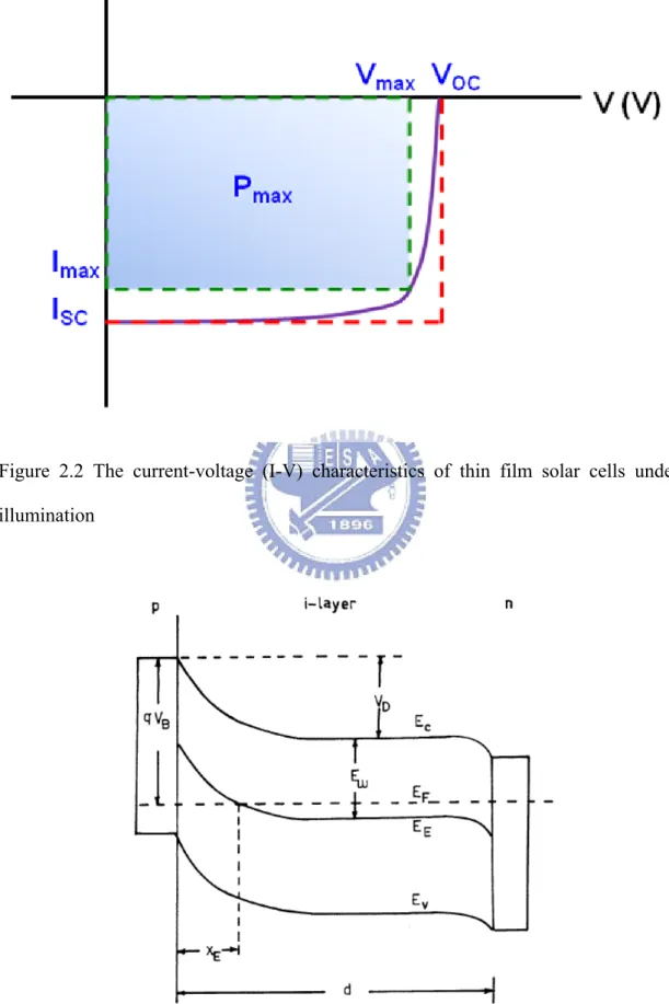
(21) depending on deposition conditions, and causes interfacial roughness.[31] The resultant optical scattering for different wavelengths can cause improvements in the photoresponse of the devices.. Back contact For amorphous silicon devices, the back contacts are formed on n-type semiconductor (and hence higher work function metals are not required) using Ag or Al. However the use of Ag or Al directly on n-type semiconductor will result in optical losses in the long-wavelength region. The long-wavelength response of the device will be improved if the n/metal interface reflects the long-wavelength radiation back to the cell. Thus the back contact for both p–i–n and n–i–p configuration is often formed with double-layer back reflector consisting of ZnO and Ag or Al. The low index ZnO layer will effectively increase the total internal reflection from the n- ZnO interface. The optical and electrical properties of the ZnO layer play a significant role in improving the back reflection properties and also the device performance.. 2.2 Parameter of Solar Cells When the cell is exposed to the solar spectrum, a photon that has an energy less than the bandgap energy greater than than. makes no contribution to the cell output. A photon that has contributes an energy. to the cell output. Energy greater. is wasted as heat. In order to the power conversion efficiency of a solar cell, current -voltage (J-V). characteristics of thin film solar cells under illumination are considered, which is shown in Figure 2.2. Current-voltage characterization means determination of the basic parameters V , J , fill factor, and efficiency (η) which are determined by only three points on the J–V curve. While these parameters are well accepted indicators of 9.
(22) solar cell performance and are particularly valuable for comparing and qualifying cells, there is a wealth of additional information that can be obtained by analyzing the entire J–V curve The open-circuit voltage,. , is the maximum photovoltaic that can be. generated in the cell and corresponds to the voltage where current is zero under illumination. The maximum current that can run through the cell at zero applied voltage is called the short-circuit current,. . The shaded area in the figure is the. maximum-power rectangle. Also defined in Figure 2.2 are the quantities I V. and. that correspond to the current and voltage, respectively, for the maximum. power output P. I. V. The power conversion efficiency of a solar cell is given by η where P. P P. I. V. I. P. V P. F. F. is the incident power and F.F is the fill factor defined as F. F. I I. V V. The fill factor is the ratio of the maximum power rectangle (shaded area) to the rectangle of I. V .. The essential parameter which determine the power conversion efficiency of thin film solar cell devices are the sort-circuit current (. ), the open-circuit voltage (. ),. and the fill factor (F.F). 2.3 Drive-level capacitance profiling model Drive-level capacitance profiling (DLCP) is an alternate technique for measuring the energetic and spatial distribution of defects in the band gap [8].The DLCP method examines the junction capacitance dependence over a range of ac voltage amplitudes 10.
(23) in addition to a range of dc bias, to obtain more information about the film response than is available from the aforementioned C–V. This technique has previously been employed to study the density of states in amorphous silicon thin films, and has greatly contributed to understanding the electronic properties of that material [32-34]. Here, we illustrate how it can also be very useful in studying microcrystalline silicon (μc-Si) films. The frequency, temperature and band bending in the sample determine the ac junction capacitance. Only those states whose thermal emission rate r is faster than 1/. can respond during a cycle of the ac applied voltage and contribute to the. measured capacitance. These states lie between the contour level EE and the conduction band mobility edge EC , as shown in Figure 2.3-1. This level is determined by setting. to give ln. Here. (1). is the Boltzmann constant, T is the absolute temperature and. is the. escape frequency ( 1013 rad s−1). Above this contour the filled states can equilibrate with the conduction band within the ac period; below this contour the filled states are frozen out and are unresponsive. Figure 2.3-1 also shows a characteristic length where. is given. = ln. where. /. ln. (2). is a characteristic screening length.. potential and. , all filled states are unresponsive; for. ε/. , all states up to. can respond.. functions as a dielectric with capacitance per unit area of. and ε is the dielectric constant. The region. charge capacitance. is the diffusion. 0 corresponds to reverse bias). For. is the applied bias (. The region 0. ,. ε. /. where. and 11. contributes a space. are the electric field and charge.
(24) density at. , respectively. These two regions constitute two capacitors in series;. finally, the junction capacitance is given by. 1 /. 1 /. 1. (3) Equation (3) is valid for any charge or profile. The drive-level capacitance method, which combines the temperature, frequency and dc bias dependence of the deep state response in one technique with the ac test signal amplitude (. ) as an additional independent variable, is experimentally. described here. This parameter (. ) was fixed in other admittance methods and the. transfer function may be assumed to be linear for such small test signals. In the case where the amplitude of the alternating voltage (. ) applied on a junction is. negligible compared with the dc bias and diffusion voltage, the junction capacitance is given by equation (3). If. is not negligible relative to the diffusion voltage it. gives higher order corrections to the junction capacitance. Specifically, (4) where. is given by equation (3).The first-order coefficient is (5). The drive-level integrated defect state density. is defined in terms of. and. as (6) Where q is the magnitude of the elemental charge, and ε is the dielectric constant, and A is the sample area. The coefficients. and. are obtained by fitting a quadratic to C versus 12. ,.
(25) as shown in figure 2.3-2. To obtain the defect profile, measurements are made as a function of bias, and NDL is plotted versus the depletion width (W), as shown in figure 2.3-3. The depletion width is measured from the junction. /. (7). The defect density corresponds most closely to the density at the edge of the depletion width.. 13.
(26) Chapter 3 Fabrication and measurement for amorphous silicon thin film solar cell 3.1 Experimental Procedures In this thesis, we employed the structure of the superstrate p-i-n hydrogenated amorphous silicon solar cells, and the solar cell structure employed was glass (Asahi's textured TCO Glass)/front ZnO/p-i-n/back ZnO/Ag with an active of 0.25 cm2. The device deposition condition: front ZnO contact layer was deposited ZnO:Ga with 20 nm thickness by sputter. All (a-Si:H) p, i, and n layers were subsequently deposited with very high frequency plasma enhanced chemical vapor deposition (VHF-PECVD) [3.13-17] multi-chamber system at 40 MHz. In deposition window layer (P-layer) process, the p-layer were deposited μc-Si:B and a-SiC:B and a-SiO:B thin films with 20 nm thickness at different devices, respectively. The intrinsic layer was deposited a-Si:H with 400 nm thickness. The n-layer was deposited a-Si:P with 30 nm thickness. Back ZnO contact layer was deposited ZnO:Ga with 100 nm thickness by sputter. Back Silver metal layer was deposited Ag with 200 nm thickness. The solar cells were characterized by current–voltage (J–V) under standard air mass 1.5 (100mW/cm2) illuminations. The current-voltage characteristic measurement of thin film solar cell devices was performed by Agilent 4156, capacitance profiling by drive level capacitance profiling methods have been carried out by using an HP 4284A impedance meter.. 3.2 Results and Discussion Figure 3.1 shows current-voltage characteristics of amorphous silicon thin film solar cells under standard illumination conditions. These devices were varied films for window layer, and the films represent μc-Si and a-SiC and a-SiO, respectively. We 14.
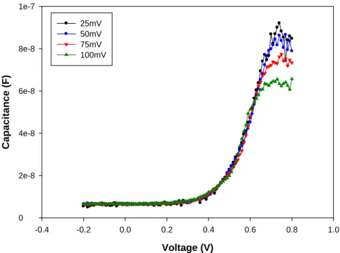
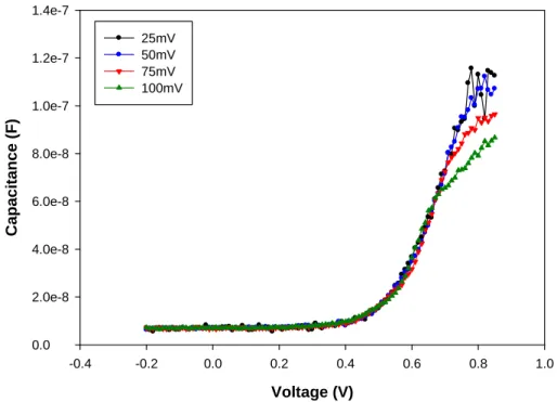
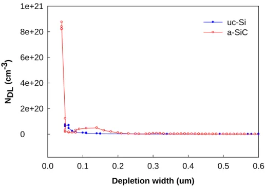
(27) could observe that open circuit voltage (Voc) is maximum for a-SiO window layer; and is medium for a-SiC window layer; and is minimum for μc-Si window layer. However, shirt circuit current (Jsc) is maximum for μc-Si window layer; and is medium for a-SiO window layer; and is minimum for a-SiC window layer. Table 3-1 summarizes the illuminated J–V parameters of a-Si:H p–i–n solar cells obtained for varied window layers. Because the value of Voc is the difference between EFn and EFp and energy band gap (Eg) which is larger could extend the difference between EFn and EFp. And energy band gap of a-SiC window layer is larger than of μc-Si window layer. Hence, the larger Eg would obtain the larger Voc for a-SiC window layer. Although the value of Jsc for a-SiC window layers is poorer than for μc-Si window layer, the whole of conversion efficiency have improve. Here the reason for Jsc have dropped, we deduce that this phenomenon are associated with the quality of intrinsic layers and the conductivity for window layer. Follow-up, we would make use of a technique of drive-level capacitance profiling (DLCP) measurement to examine the quality of intrinsic layers. Figure 3.2(a)-3.4(a) show typical capacitance-voltage curve of the variation of junction capacitance with 100Hz for varied window layers of p-i-n a-Si solar cells at room temperature, respectively. Figure 3.2(b)-3.4(b) show NDL versus depletion width for varied window layers of p-i-n a-Si solar cells at room temperature, respectively. We could observe that number of defects in the vicinity of the intrinsic layer of p/i interface were more than of bulk and i/n interface for all solar cells. We observe that number of defects for a-SiC window layer are more than for μc-Si window layer, result in electric field of intrinsic layer for a-SiC window layer is weaker than for μc-Si window layer, as shown in as shown in figure 3.5. Hence, the value of Jsc for a-SiC window layer is poorer than for μc-Si window layer. The another reason that the conductivity for a-SiC window layer is poorer than for μc-Si window layer, then 15.
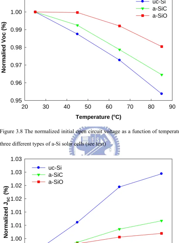
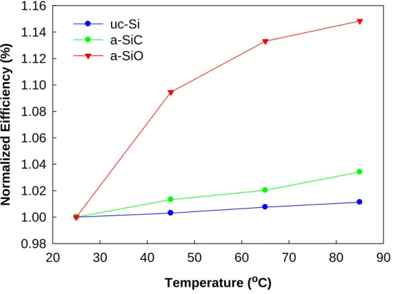
(28) the value of Jsc for a-SiC window layers is poorer than for μc-Si window layer. In order to improve conversion efficiency further, we employ to increase electric conductivity for window layer. We adopt a-SiO material as window layer to improve Jsc. The result that have not only improve Jsc and Voc but also improve conversion efficiency. From DLCP analysis, We observe that number of defects for a-SiO window layer are less than for a-SiC window layer, as shown in figure 3.6. Although the value of Jsc for a-SiO window layer increase, it is not better than for μc-Si window layer. The conductivity for μc-Si window layer is lower than for a-SiO window layer after all. Figure 3.7 show the measured values of current-voltage characteristics for a-Si thin film solar cells with temperature measurement from 25℃ to 85℃ under standard illumination conditions. We could observe with the value of Voc decrease as the temperature increase, as shown in figure 3.8; with the value of Jsc increase as the temperature increase, as shown in figure 3.9; with the value of conversion efficiency increase as the temperature increase, as shown in figure 3.10 .The first, Voc is associated with energy band gap Eg, is given by eV. EF. EF. E. kTln. G bR N N. where Eg is the energy band gap G is the generation rate bR is the recombination rate coefficient NV is effective density of states in the valence band NC is effective density of states in the conduction band k is Boltzmann constant T is Kevin temperature. 16.
(29) Eg is associated with temperature, and when temperature is rise with Eg is dropped. Therefore, with the value of Voc decrease when temperature is rise. Device of μc-Si of p layer reduce the maximum amount of Voc with temperature increase to 85oC and the value about 4.63%, as shown in table 3-2. The second, Jsc is associated with collect electron-hole pairs capability. Because they generate a mass of electron-hole pairs in the intrinsic layer as temperature is rise, it can collect a mass of electron-hole pairs output abundant currents. Therefore, with the value of Jsc increase when temperature is rise. Device of μc-Si of p layer increase the maximum amount of Jsc with temperature increase to 85oC and the value about 2.94%. The last, conversion efficiency is associated with Voc and Jsc. Although with the value of Voc decrease as temperature is rise, with the value of Jsc increase more than the value of Voc decrease as temperature is rise. The whole of conversion efficiency improve as temperature rise. Device of a-SiO of p layer increase the maximum amount of conversion efficiency with temperature increase to 85oC and the value about 14.8%. According to the above results, Device of a-SiO of p layer is the most sensitive to temperature. Figure 3.11 show the measured values of current-voltage characteristics for a-Si thin film solar cells with temperature measurement from 25℃ to 85℃ under the condition of darkness. We could observe that current density increase as the temperature of solar cells increase for any temperature condition. Under the forward bias, we would observe change in current density rise is not the same in the voltage region of 0.1~0.5V and 0.7~0.8V and 1.2~1.3V. The characteristics of solar cells and pn diodes are the same under the condition of darkness. The current-voltage characteristics of ideal diodes are given by J. J Exp. V KT. 1. (1). 17.
(30) When the ideal diffusion current dominates, n equals 1; whereas when the recombination current dominates, n equals 2.Therefore, we attempt to extract the value of n by fitting from eq. (1) in the voltage region of 0.1~0.5V and 0.7~0.8V and 1.2~1.3V, respectively, and shown in Table 3-3. In the voltage region of 0.1~0.5V and 0.7~0.8V and 1.2~1.3V, Jo also increased with increasing temperature for the cell, so temperature dependence of Jo. However, the value of n is greater than 1 for all cells. This phenomenon could be associated with series resistance effect or other factor effects. Hence, current increases more gradually with forward voltage.. 18.
(31) Chapter 4 Fabrication and measurement for microcrystalline silicon thin film solar cell 4.1 Experimental Procedures In this thesis, we employed the structure of the superstrate p-i-n hydrogenated microcrystalline silicon solar cells, and the solar cell structure employed was glass (Asahi's textured TCO Glass)/front ZnO/p-i-n/back ZnO/Ag with an active of 0.25 cm2. The device deposition condition: front ZnO contact layer was deposited ZnO:Ga with 40nm thickness by sputter. All (μc-Si:H) p, i, and n layers were subsequently deposited by 40 MHz in the very high frequency plasma enhanced chemical vapor deposition (VHF-PECVD) multi-chamber system. The window layer (P-layer) was deposited μc-Si:B with 15 nm thickness. The intrinsic layer was deposited μc-Si with 1500 nm thickness. The n-layer was deposited μc-Si:P with 15 nm thickness. Back ZnO contact layer was deposited ZnO:Ga with 100 nm thickness by sputter. Back Silver metal layer was deposited Ag with 200 nm thickness. In VHF-PECVD process, we use a H2 and SiH4 gases. Application of high-rate μc-Si:H deposition was most feasible to promote electron-impact dissociation of SiH4 and H2 into SiH2 (SiH H. SiH ). The dilution ratios R. H /SiH. were 1000/22 and 1000/14 and. 1000/13 for μc-Si:H intrinsic layer at pressures of 4Torr、6Torr、8Torr, respectively. The solar cells were characterized by current–voltage (J–V) and spectral response measurements [40] under standard air mass 1.5 (100 mW/cm2) illuminations. The current-voltage characteristic measurement of thin film solar cell devices was performed by Agilent 4156, capacitance profiling by drive level capacitance profiling methods have been carried out by using an HP 4284A impedance meter. Otherwise, we make the conductivity and activation energy measurement of μc-Si:H intrinsic layer, and measurement flow:the voltage sweep 0V to 10V and select a constant 19.
(32) voltage, V (mostly 10 V) is applied over the contacts and the current, I, is measured. We use equation of dark conductivity, σ. I V. W L. D. where I is measured current V is applied voltage W is width of the film L is length of the film D is thickness of the film to find dark conductivity. We make the sample to heat from 300K to 370K for temperature measurements, and employ equation of activation energy, σ. σ Exp. E KT. where σ is the coefficient of conductivity Ea is activation energy to find activation energy of the sample.. 4.2 Results and Discussion Figure 4.1 shows current-voltage characteristics of microcrystalline silicon thin film solar cells under standard illumination conditions. These devices were deposited in different pressures. We could observe that short circuit current density (J ) and conversion efficiency (η) increased when deposition pressure increased, and shunt resistance (R ) and series resistance (R ) decrease when deposition pressure increase, but open circuit voltage (V ) was almost same. Table 4-1 summarizes the illuminated J–V parameters of μc-Si:H p–i–n solar cells obtained for varied i layer deposition rates. Figure 4.2 shows the Quantum efficiency (QE) for several high-efficiency thin 20.
(33) film solar cells. Spectral response measurements are valuable to characterize the photocurrent and are commonly used to determine the losses responsible for reducing the measured short circuit current density from the maximum achievable photocurrent. QE is a dimensionless parameter given by the number of electrons which exit the device per incident photon at each wavelength. Device losses measured by QE can be optical, due to the front reflection and absorption in the window, transparent conductor, and other layers, or electronic, due to recombination losses in the absorber. We could observe that at pressures of 4、6Torr and pressures of 8Torr which corresponded to QE were approximately the same, respectively, in short wavelength region. Because we varied thicknesses of deposited p-type microcrystalline silicon layer, and the deposition thicknesses were thinner slightly at pressures of 8Torr than at pressures of 4、6Torr. They could decrease absorption losses in the thinner thickness, and could increase the number of electrons which exit the device per incident photon. Hence, the thinner thicknesses were higher QE. On the other hand, in long wavelength region, we could observe that the deposition pressure increased and QE also increased. The reason that lower deposition pressure of the thin films would deposited rate slowly, result in more oxygen go into the thin films, and oxygen could generate electron as donors when it went into the thin films, then oxygen would be trapped in the vicinity of grain boundaries.[41] Hence, the thin films resulted in tending to n- quality gradually. The result that almost made built in field totally locate in the vicinity of p/i interface, and caused built in field to become weak in the vicinity of i-layer bulk and i/n interface, as shown in Figure 4.3. Because the photocurrent was proportional to built in field, the thin films of lower deposition pressure were lower photocurrent. In order to verify high-rate deposition can decrease oxygen go into the film, we make the conductivity and activation energy measurement of μc-Si intrinsic layer. 21.
(34) Figure 4.4 shows dark conductivity and photo conductivity as a function of deposition pressure. We observe that with dark conductivity and photo conductivity decrease as deposition pressure increase. It indicates obviously smaller resistance and better conductivity for low deposition pressure, and characteristic of the film is tending to nquality. Figure 4.5 shows activation energy as a function of deposition pressure. We observe that with activation energy increases as deposition pressure increases, and the value of activation energy is close to 550 meV for 8Torr deposition pressure, as shown in Table4-2. Energy band gap of μc-Si film is about 1.12eV and midgap of μc-Si film is about 550 meV, and activation energy is close to 550 meV for 8Torr deposition pressure, so Fermi level EF of μc-Si film is close to Ei for high deposition pressure. Yet, the value activation energy is 478 meV and Fermi level EF of μc-Si film is above Ei for 4Torr deposition pressure. Therefore, characteristic of μc-Si film is tending to n- quality for 4Torr deposition pressure. Hence, high deposition pressure not only made characteristic of the film tending to intrinsic quality but also could decrease oxygen go into the film. In brief, the thinner thicknesses of deposited p-type microcrystalline silicon layer were higher QE and independent on deposition pressures in short wavelength region; lower deposition pressure of the thin films would more oxygen go into the thin films, then the thin films made tending to n- quality gradually result in almost make electric field totally locate in the vicinity of p/i interface, and the photocurrent was proportional to built in field. Therefore, the thin films of lower deposition pressure were lower photocurrent in long wavelength region. In addition, in order to investigate about the relationship between the spatial distribution of defects in the intrinsic layer and the deposition pressure, we would make use of a technique of drive-level capacitance profiling (DLCP) for varied deposition pressures. 22.
(35) Figure 4.6(a)-4.8(a) show typical capacitance-voltage curve of the variation of junction capacitance with 100Hz for deposition pressures of 4-8Torr at room temperature, respectively. Figure 4.6(b)-4.8(b) show NDL versus depletion width for deposition pressures of 4-8Torr at room temperature, respectively. We could observe that number of defects in the vicinity of the intrinsic layer of p/i interface were lower for higher deposition pressures; however, number of defects in the intrinsic layer of bulk and i/n interface were not any variation explicitly for arbitrarily deposition pressures, as shown in Figure 4.9. Because gas of the lower deposition pressures was less reactants than the higher deposition pressures and generated less precursors, and there had prone to plasma ion bombardment more probability in the vicinity of p/i interface, result in the destruction of the interface is very serious. Hence, it is better in the interface for higher pressure deposition. [42] Figure 4.10 show the measured values of current-voltage characteristics for μc-Si thin film solar cells with temperature measurement from 25℃ to 85℃ under the condition of darkness. We could observe that current density increase as the temperature of solar cells increase for any temperature condition. Under the forward bias, we would observe change in current density rise are different in the voltage region of 0.2V~0.4V and 0.6~1V. The characteristics of solar cells and pn diodes are the same under the condition of darkness. The current-voltage characteristics of ideal diodes are given by J. J Exp. V KT. 1. (1). where Jo is the saturation current density n is the ideality factor. When the ideal diffusion current dominates, n equals 1; whereas when the recombination current dominates, n equals 2.Therefore, we attempt to extract the 23.
(36) value of n by fitting from eq. (1) in the voltage region of 0.2V~0.4V and0.6~1V, respectively, and shown in Table 4-3. Jo increased with increasing temperature for all cells, and the value of n is 2 approximately for all cells in the voltage region of 0.2V~0.4V. The result show temperature dependence of Jo and ideality factor n equals 2 approximately represents the quality of the recombination center. So that is recombination current dominant in the voltage region of 0.2V~0.4V. In the voltage region of 0.6~1V, Jo also increased with increasing temperature for all cells, so temperature dependence of Jo. However, the value of n is greater than 1 for all cells. This phenomenon is associated with series resistance effect. At low current level, the IR drop across the neutral regions is usually small compared to kT/q (26 mV at 300K), where I is the forward current and R is the series resistance. At high current level, the IR drop across the neutral regions is very large, and the neutral regions of i layer is huge specifically. Hence, current increases more gradually with forward voltage. Figure 4.11 show the measured values of current-voltage characteristics for μc-Si thin film solar cells with temperature measurement from 25℃ to 85℃ under standard illumination conditions. We could observe with the value of Voc decrease as the temperature increase, as shown in Figure 4.12; with the value of Jsc increase as the temperature increase, as shown in Figure 4.13; with the value of conversion efficiency decrease as the temperature increase, as shown in Figure 4.14. The first, Voc is associated with energy band gap Eg, is given by eV. EF. EF. E. kTln. G bR N N. Eg is associated with temperature, and when temperature is rise with Eg is dropped. Therefore, with the value of Voc decrease when temperature is rise. Device of 4Torr deposition pressure reduce the maximum amount of Voc with temperature increase to 85oC and the value about 11.5%, as shown in table 4-4. The second, Jsc is associated 24.
(37) with collect electron-hole pairs capability. Because they generate a mass of electron-hole pairs in the intrinsic layer as temperature is rise, it can collect a mass of electron-hole pairs output abundant currents. Therefore, with the value of Jsc increase when temperature is rise. Device of 8Torr deposition pressure increase the maximum amount of Jsc with temperature increase to 85oC and the value about 2.94%. The last, conversion efficiency is associated with Voc and Jsc. Although with the value of Jsc increase as temperature is rise, with the value of Voc decrease more than the value of Jsc increase as temperature is rise. The whole of conversion efficiency decayed as temperature rise. Device of 4Torr deposition pressure decrease the maximum amount of conversion efficiency with temperature increase to 85oC and the value about 14.8%. According to the above results, Device of a-SiO of p layer is the most sensitive to temperature.. 25.
(38) Chapter 5 Conclusion We succeed in introducing optimum window layer material to fabricate a-Si:H solar cells. The solar cells of window layer which used high energy band gap material would improve Voc and conversion efficiency. The window layer of a-SiO which is a kind of high energy band gap material is effective in obtaining high Voc. The maximum efficiency obtained so far is 5.75%. In addition, we have shown that deposition pressure plays a key role in determining Jsc of μc-Si:H solar cells fabricated using high deposition rate plasma process. High pressure deposition at 8Torr is effective in obtaining high Jsc. The maximum efficiency obtained so far is 5.045%. We propose that low oxygen concentration behavior associated with the microstructure of high pressure grown μc-Si:H is responsible for the excellent charge collection behavior in p-i-n junction solar cells. Otherwise, we also succeed in utilizing a method technology of DLCP to extract number of detects from intrinsic layer for thin film solar cells. High deposition pressure is effective in suppressing number of detects in the vicinity of p/i interface.. 26.
(39) Reference [1]. M.A. Green. Photovoltaics : technology overview. Energy Policy; 28: 989-998, 2000 [2]. H.Sakai,T. Yoshida, s. Fujikake, T. Hama, and Y. lchikawa. Effect of p/I interface layer on dark J-V characteristics and Voc in p-i-n a-Si solar cells. Journal of Applied Physics; 67(7):3494-3499, 1990 [3]. S. Guha, J. Yang, P. Nath, and M. Hack. Enhancement of open circuit voltage in high efficiency amorphous silicon alloy solar cells Applied Physics Letters ; 49:218, 1986 [4]. W. Ma, T. Saida, C. C. Lim, S. Aoyama, H. Okamoto, and Y. Hamakawa. Proceedings of the First World Conference on Photovoltaic Solar Energy Conversion, Hawaii. IEEE; 417,.1994 [5]. J. K. Rath, C. H. M. Van der Werf, F. A. Rubinelli, and R. E. I. Schropp,25th IEEE Photovoltaic Specialists’ Conference, Washington DC, IEEE, New York, , p. 1101, 1996 [6]. J. K. Rath and R. E. I. Schropp, Sol. Energy Mater. Sol. Cells; 53:189. 1998 [7]. S.Veprek, F-A. Sarrot, S. Rambert, and E. Taglauer,J.Vac.Sci. Technol.A.; 7:2614, 1989 [8]. Michelson C E, Gelatos A V and Cohen J D .Drive-level capacitance profilingIts application to determining gap state densities in hydrogenated amorphous silicon films. Applied Physics Letters; 47 (4): 412, 1985 [9]. Chopra KL, Major S, Pandya DK. Transparent conductors–a status review. Thin Solid Films; 102 (1): 1–46, 1983 [10]. Major S, Kumar S, Bhatnagar M, Chopra KL. Effect of hydrogen plasma treatment on transparent conducting oxides. Applied Physics Letters; 49: 27.
(40) 394–396, 1986 [11]. Major S, Chopra KL. Indium-doped zinc oxide films as transparent electrodes for solar cells. Solar Energy Materials; 17 (5): 319–327, 1988 [12]. Gordon RG. Criteria for choosing transparent conductors. MRS Bulletin; 52–57, 2000 [13]. Ginley DS, Bright C. Transparent conducting oxides. MRS Bulletin; 15–18, 2000 [14]. Romeo N, Bosio A, Canevari V, Terheggen M, Vaillant RL. Comparison of different conducting oxides as substrates for CdS/CdTe thin-film solar cells. Thin Solid Films; 431–432: 364–368, 2003 [15]. McCandless BE, Hegedus SS. Influence of CdS window layer on thin-film CdS/CdTe solar cell performance. Proceedings of the 22th IEEE Photovoltaic Specialists Conference ; 967–972, 1991 [16]. Tawada T, Kondo M, Okamoto H, Hamakawa Y. Hydrogenated amorphous silicon carbide as a window material for high efficiency a-Si solar cells. Solar Energy Materials; 6: 299–315, 1982 [17]. Tsu DV, Chao BS, Ovshinsky SR, Guha S, Yang J. Effect of hydrogen dilution on the structure of amorphous silicon alloys. Applied Physics Letters; 71: 1317–1319, 1997 [18]. Mahan AH, Yang J, Guha S,Williamson DL. Structural changes in a-Si:H film crystallinity with high dilution. Physical Review B; 61: 1677–1680, 2000 [19]. Yamamoto K, Nakashima A, Suzuki T, Yoshimi M, Nishio H, Izumina M. Thin-film polycrystalline Si solar cell on glass substrate fabricated by a novel low temperature process. Japan Journal of Applied Physics; 33: L1751, 1994 [20]. Chen W, Sopori B, Jones K, Reedy R, Ravindra NM, Aparicio R, Birkmire RW, Morrison S, Coats SK, Madan A.Optically assisted metal-induced crystallization 28.
(41) of thin Si films for low-cost solar cells. Proceedings of the MRS SpringMeeting Vol. 685E: D3.2.1–6. Pittsburgh, 2001 [21]. Basore PA. Pilot production of thin-film crystalline silicon on glass modules. Proceedings of the 29th IEEE Photovoltaic Specialists Conference, 2002; 49–52. [22]. Mahan AH. Hot wire chemical vapour deposition of Si containing materials for solar cells. Solar Energy Materials and Solar Cells; 78(1–4): 299–327, 2003 [23]. Wang TH, Ciszek TF, Page MR, Bauer RE, Wang Q, Landry MD. APIVT-grown silicon thin layers and PV devices. Proceedings of the 29th IEEE Photovoltaic Specialists Conference; 94–97, 2002 [24]. Rath JK. Low temperature polycrystalline silicon: a review on deposition, physical properties and solar cell applications. Solar Energy Materials and Solar Cells; 76 (4): 431–487, 2003 [25]. Bergmann RB, Rinke TJ. Perspectives of crystalline Si thin-film solar cells: a new era of thin monocrystalline Si films.Progress in Photvoltaics Research and Applications; 8: 451–464, 2000 [26]. Powell MJ, Deane SC. Defect-pool model and the hydrogen density of states in hydrogenated amorphous silicon. Physical Review B; 53(15): 0121–10132, 1996 [27]. Carlson DE, Chen LF, Ganguly G, Lin G, Middya AR, Crandall RS, Reedy R. MRS Proceedings; 557: 395, 1999 [28]. Dutta V, Murthy RVR. An approach to study band-gap and interface states in a Si: H p-i-n solar cells. Japan Journal of Applied Physics 1997; 36: 6687. [29]. Jiang L, Lyou JH, Rane S, Schiff EA, Wang Q, Yuon Q. MRS Proceedings; 609: A18.3.1–8 , 2000 [30]. Wang Q, Iwaniczko E, Xu Y, Gao W, Nelson BP, Mahan AH, Crandall RS, Branz HM. MRS Proceedings; 609:A4.3.1–6, 2000 29.
(42) [31]. Zeman M, Van Swaaij RACMM, Zuiddam M, Metselaar JW, Schropp REI. MRS Proceedings; 557: 725, 1999 [32]. K. K. Mahavadi, K. Zellama, J. D. Cohen, and J. P. Harbison. Light-induced defect creation in hydrogenated amorphous silicon: A detailed examination using junction-capacitance methods. Physical Review B; 35: 7776-7779, 1987 [33]. T. Unold and J. D. Cohen. Enhancement of light-induced degradation in hydrogenated amorphous silicon due to carbon impurities. Applied Physics Letters; 58: 723-725, 1991 [34]. T. Unold, J. Hautala, and J. D. Cohen. Effect of carbon impurities on the density of states and the stability of hydrogenated amorphous silicon. Physical Review B; 50 (23): 16985-16994, 1994 [35]. M. Fukawa, S. Suzuki, L. Guo, M. Kondo, and A. Matsuda, Sol. Energy Mater. Sol. Cells; 66:217, 2001 [36]. A. Lambertz, O. Vetterl, and F. Finger, Proc. of the 17th European Photovoltaic Solar Energy Conference, Munich, Germany, 22–26 Oct. 2001, edited by B. McNelis,W. Palz, H. A. Ossenbrink, and P. Helm (WIPMunich & ETA-Florence, , p. 2977, 2001 [37]. T. Matsui, M. Tsukiji, H. Saika, T. Toyama, and H. Okamoto, Jpn. J. Appl. Phys.; Part 1 41:20, 2002 [38]. U. Graf, J. Meier, U. Kroll, J. Bailat, C. Droz, E. Vallat-Sauvain, and A.Shah, Thin Solid Films; 427: 37 , 2003 [39]. Y. Mai, S. Klein, X. Geng, and F. Finger, Apply Physic Letter; 85, 2004 [40]. Emery K. Measurement and characterization of solar cells and modules. In Handbook of Photovoltaic Science and Engineering, Luque A, Hegedus S (eds). Wiley: Chichester; Chap. 16, 2003 [41]. Takuya Matsui, Akihisa Matsuda, Michio Kondo, High-rate microcrystalline 30.
(43) silicon deposition for p-i-n junction solar cells, Solar energy materials & solar cells; 90:3199-3204, 2006 [42].Y.Mai, S.Klein, R. Carius, J. Wolff, A. Lambertz, and F. Finger, X.Geng, microcrystalline silicon solar cells deposited at high rates. Journal of applied physics; 97:114913, 2005. 31.
(44) Figure. Figure 2.1(a) The type of superstrate solar cells structure. Figure 2.1(b) The type of substrate solar cells structure. 32.
(45) Figure 2.2 The current-voltage (I-V) characteristics of thin film solar cells under illumination. Figure 2.3-1 Band diagram of p-i-n junction 33.
(46) Figure 2.3-2 Variation of junction capacitance with alternation voltage drive level. Figure 2.3-3 Drive level charge density versus depletion width in the solar cell. 34.
(47) 2. 15. 10. 5. -0.4. -0.2. Current density (mA/cm ). P_uc-Si P_SiC P_SiO. 0 0.0. 0.2. -5. 0.4. 0.6. 0.8. 1.0. Voltage (V). -10. -15. Figure 3.1 shows current-voltage characteristics of amorphous silicon thin film solar cells under standard illumination conditions. 35.
(48) 5e-8 25mV 50mV 75mV 100mV. Capacitance (F). 4e-8. 3e-8. 2e-8. 1e-8. 0. -0.4. -0.2. 0.0. 0.2. 0.4. 0.6. 0.8. Voltage (V). Figure 3.2(a) Capacitance vs. dc bias for μc-Si window layer of solar cell. The measuring frequency is 100Hz and the temperature is 300K.The amplitude of the alternating voltage is 25mV、50 mV、75 mV、100 mV, respectively 8e+19 uc-Si. NDL (cm-3). 6e+19. 4e+19. 2e+19. 0. 0.0. 0.1. 0.2. 0.3. 0.4. 0.5. 0.6. Depletion width (um). Figure 3.2(b) Drive level charge density versus depletion width in the solar cell depicted in Figure 3.2(a). 36.
(49) 1e-7 25mV 50mV 75mV 100mV. Capacitance (F). 8e-8. 6e-8. 4e-8. 2e-8. 0 -0.4. -0.2. 0.0. 0.2. 0.4. 0.6. 0.8. 1.0. Voltage (V). Figure 3.3(a) Capacitance vs. dc bias for a-SiC window layer of solar cell. The measuring frequency is 100Hz and the temperature is 300K.The amplitude of the alternating voltage is 25mV、50 mV、75 mV、100 mV, respectively 1e+21 a-SiC. NDL (cm-3). 8e+20 6e+20 4e+20 2e+20 0. 0.0. 0.1. 0.2. 0.3. 0.4. 0.5. 0.6. Depletion width (um). Figure 3.3(b) Drive level charge density versus depletion width in the solar cell depicted in Figure 3.3(a). 37.
(50) 1.4e-7 25mV 50mV 75mV 100mV. 1.2e-7. Capacitance (F). 1.0e-7. 8.0e-8. 6.0e-8. 4.0e-8. 2.0e-8. 0.0 -0.4. -0.2. 0.0. 0.2. 0.4. 0.6. 0.8. 1.0. Voltage (V). Figure 3.4(a) Capacitance vs. dc bias for a-SiO window layer of solar cell. The measuring frequency is 100Hz and the temperature is 300K.The amplitude of the alternating voltage is 25mV、50 mV、75 mV、100 mV, respectively 8e+20 a-SiO. NDL (cm-3). 6e+20. 4e+20. 2e+20. 0. 0.0. 0.1. 0.2. 0.3. 0.4. 0.5. 0.6. Depletion width (um). Figure 3.4(b) Drive level charge density versus depletion width in the solar cell depicted in Figure 3.4(a). 38.
(51) 1e+21 uc-Si a-SiC. NDL (cm-3). 8e+20 6e+20 4e+20 2e+20 0. 0.0. 0.1. 0.2. 0.3. 0.4. 0.5. 0.6. Depletion width (um). Figure 3.5 Drive level charge density as a function of depletion width of two different types of a-Si solar cells (see text). 1e+21 a-SiC a-SiO. NDL (cm-3). 8e+20 6e+20 4e+20 2e+20 0. 0.0. 0.1. 0.2. 0.3. 0.4. 0.5. 0.6. Depletion width (um). Figure 3.6 Drive level charge density as a function of depletion width of two different types of a-Si solar cells (see text). 39.
(52) 2 Current density (mA/cm ). O. 25 C O 45 C O 65 C O 85 C. 15. 10. 5. -0.4. 0 0.0. -0.2. 0.2. 0.4. 0.6. 0.8. 1.0. Voltage (V). -5. -10. -15. O. 25 C O 45 C O 65 C O 85 C. 15. 10. 5. -0.4. 2 Current density (mA/cm ). (a). 0 0.0. -0.2. 0.2. 0.4. 0.6. 0.8. 1.0. Voltage (V). -5. -10. -15. O. 25 C O 45 C O 65 C O 85 C. 15. 10. 5. -0.4. -0.2. 0 0.0. 2 Current density (mA/cm ). (b). 0.2. 0.4. 0.6. 0.8. 1.0. Voltage (V). -5. -10. -15. (c) Figure 3.7 Illuminated J-V parameters of a-Si p-i-n solar cells by temperature measurement a-Si p-i-n solar cells for deposited p layers (a)μc-Si, (b) a-SiC, (c)a-SiO. 40.
(53) 1.01 uc-Si a-SiC a-SiO. Normalied Voc (%). 1.00 0.99 0.98 0.97 0.96 0.95 20. 30. 40. 50. 60. 70. 80. 90. Temperature (oC) Figure 3.8 The normalized initial open circuit voltage as a function of temperature of three different types of a-Si solar cells (see text). 1.03. Normalized JSC (%). 1.03 1.02. uc-Si a-SiC a-SiO. 1.02 1.01 1.01 1.00 1.00 1.00 20. 30. 40. 50. 60. 70. 80. 90. Temperature (oC) Figure 3.9 The normalized initial short circuit current as a function of temperature of three different types of a-Si solar cells (see text) 41.
(54) 1.16 uc-Si a-SiC a-SiO. Normalized Eifficiency (%). 1.14 1.12 1.10 1.08 1.06 1.04 1.02 1.00 0.98 20. 30. 40. 50. 60. 70. 80. 90. Temperature (oC) Figure 3.10 The normalized initial conversion efficiency as a function of temperature of three different types of a-Si solar cells (see text) 1e+1. Current density (A/cm2). 1e+0. 25 OC 65 OC 85 OC. 1e-1 1e-2 1e-3 1e-4 1e-5 1e-6 0.0. 0.5. 1.0. 1.5. 2.0. 2.5. Voltage (V) Figure 3.11 Forward bias J-V characteristics for a-Si solar cells with different temperature 42.
(55) 2. 15 10 5. -0.4. -0.3. Current Density (mA/cm ). 4Torr 6Torr 8Torr. -0.2. -0.1. 0 0.0. 0.1. 0.2. 0.3. -5. 0.4. 0.5. 0.6. Voltage (V). -10 -15 -20. Figure 4.1 Current-voltage (J-V) characteristics of μc-Si solar cells under standard illumination conditions. 100. 4Torr 6Torr 8Torr. Quantum Efficiency (%). 90 80 70 60 50 40 30 20 10 0 400. 600. 800. 1000. Wavelength (nm). Figure 4.2 Quantum efficiency spectra for μc-Si solar cells prepared at different i-layer deposition pressures 43.
(56) Figure 4.3 Band diagram of p-i-n junction by oxygen diffuse grain boundary process. 44.
(57) Dark conductivity (S/cm). 1E-4. 1E-5. 1E-5. 1E-6. 1E-6. 1E-7. 1E-7. 1E-8. Photo conductivity (S/cm). 1E-4. 1E-8 3. 4. 5. 6. 7. 8. 9. Pressure (Torr). Figure 4.4 Dark and photo conductivity at room temperature for μc-Si solar cells prepared at different i-layer deposition pressures. -7. 3.0x10. 600 -7. 550. -7. 2.0x10. 500. -7. 450. -7. 400. 1.5x10 1.0x10. 350. -8. 5.0x10. Activation Energy (meV). Dark conductivity (S/cm). 2.5x10. 300 0.0 250 3. 4. 5. 6. 7. 8. 9. Pressure (Torr). Figure 4.5 Dark conductivity at room temperature and activation energy measured at 300K-370K for μc-Si solar cells prepared at different i-layer deposition pressures. 45.
(58) 7e-8 25mV 50mV 75mV 100mV. 6e-8. Capcitance (F). 5e-8 4e-8 3e-8 2e-8 1e-8 0. -1.2. -1.0. -0.8. -0.6. -0.4. -0.2. 0.0. 0.2. 0.4. 0.6. 0.8. Voltage (V). Figure 4.6(a) Capacitance versus dc bias for μc-Si solar cells at i-layer deposition pressure: 4Torr. The measuring frequency is 100Hz and the temperature is 300K.The amplitude of the alternating voltage is 25mV、50 mV、75 mV、100 mV, respectively. 1.6e+20 1.4e+20. 4torr. 1.2e+20. NDL (cm-3). 1.0e+20 8.0e+19 6.0e+19 4.0e+19 2.0e+19 0.0. 0.0. 0.2. 0.4. 0.6. 0.8. 1.0. 1.2. 1.4. Depletion width (um). Figure 4.6(b) Drive level charge density versus depletion width in the solar cell depicted in Figure 4.6(a) 46.
(59) 7e-8 25mV 50mV 75mV 100mV. 6e-8. Capcitance (F). 5e-8 4e-8 3e-8 2e-8 1e-8 0. -1.2. -1.0. -0.8. -0.6. -0.4. -0.2. 0.0. 0.2. 0.4. 0.6. 0.8. Voltage (V). Figure 4.7(a) Capacitance versus dc bias for μc-Si solar cells at i-layer deposition pressure : 6Torr. The measuring frequency is 100Hz and the temperature is 300K. The amplitude of the alternating voltage is 25mV、50 mV、75 mV、100 mV, respectively. 3e+19 6torr. 3e+19. -3. NDL (cm ). 2e+19. 2e+19. 1e+19. 5e+18. 0. 0.0. 0.2. 0.4. 0.6. 0.8. 1.0. 1.2. 1.4. Depletion width (um). Figure 4.7(b) Drive level charge density versus depletion width in the solar cell depicted in Figure 4.7(a) 47.
數據
+7

相關文件
Do you want bacon and eggs?.
It’s (between/next to) the church and the
Listen - Check the right picture striped hat polka dotted hat.. Which hat do
Play - Let’s make a big family How many people are in your family1. Write it
Sam: I scraped my knee and bumped my head.. Smith: What happened
straight brown hair dark brown eyes What does he look like!. He has short
While Korean kids are learning how to ski and snowboard in the snow, Australian kids are learning how to surf and water-ski at the beach3. Some children never play in the snow
I am writing this letter because I want to make a new friend in another country.. Maybe you will come to Gibraltar
