1456
J. Electrochern. Soc., Vol. 136, No. 5, May 1989 9 The Electrochemical Society, Inc.
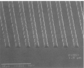
Fig. 1. A scanning electron micrograph of 1.5 ~m line and space pattern.
cially photosensitive toward p h o t o i n d u c e d cross-linking by o n i u m salts is poly(N-vinylcarbazole). Similarly, poly(vinylanthracene), poly(vinylperylene), poly(vinylphe- nanthrene), and poly(vinylpyrene) would likewise be ex- pected to undergo facile electron transfer reactions in the presence of o n i u m salt photoinitiators leading to cross- linking.
Poly(4-chlorostyrene) and poly(4-bromostyrene) are ex- amples of halogen containing polymers w h i c h are cross- linked on irradiation in the presence of photosensitive o n i u m salts.
In contrast to those polymers described above which un- dergo electron transfer induced cross-linking, polymers such as polystyrene, poly(~-methylstyrene), and poly(4- nitrostyrene) which either are not activated toward elec- tron transfer or possess deactivating electron substituents such as the nitro group are not useful as negative photore- sists. Similarly, poly(1- and 2-vinylnaphthalene) are not cross-linked u n d e r the same conditions p r e s u m a b l y be- cause their reduction potentials are not sufficiently low
enough to permit t h e m to easily undergo the required elec- tron abstraction from the naphthalene rings.
A m o r e detailed photoimaging study was carried out with poly(4-methoxystyrene) and the specifics of the pro- cedure are described in the e x p e r i m e n t a l portion of this paper. To briefly summarize, the above m e n t i o n e d poly- m e r together with the o n i u m salt, di(4-t-butylphenyl)- i o d o n i u m hexafluoroantimonate, were spin coated onto silicone wafers. After bake drying the wafers, they were subjected to imagewise exposure at 254 n m using a quartz m a s k and then baked for 30s at 130~ Finally, the unex- posed portions of the resist were r e m o v e d preferentially by i m m e r s i o n in an equal v o l u m e m i x t u r e of n-hexane and dichloromethane. In Fig. 1 is shown a scanning electron m i c r o g r a p h of 1.5 ~m line and space patterns produced using the above described process. A slight bridging can be observed in the otherwise well-resolved patterns. The patterns show some loss of line profile; however, this is to be e x p e c t e d since the postbake t e m p e r a t u r e was consider- ably above the reported Tg at 89~ (7). Perhaps m o s t strik- ing is the apparent lack of solvent induced wavyness in the pattern, usually t e r m e d "snaking," although this can be observed u n d e r conditions of low dose and in the 1-1.5 ~m features. The photoresist has an u n e x p e c t e d l y high photosensitivity since the pattern shown in Fig. 1 was m a d e at an irradiation dose of only 30 m J / c m 2.
Manuscript received April 28, 1988.
General Electric Corporate Research and Development assisted in meeting the publication costs of this article.
R E F E R E N C E S
1. J. V. Crivello, Polym. Eng. and Sci., 23, 953 (1983). 2. H. Ito and C. G. Willson, U.S. Pat., 4,491,628 (1985). 3. H. Ito, C. G. Willson, J. M. J. Frechet, M. J. Farrall, and
E. Eichler, Macromolecules, 16, 510 (1983). 4. J. V. Crivello, Adv. Polym. Sci., 62, 1 (1984).
5. J. V. Crivello and J. H. W. Lam, Macromolecules, 10, 1307 (1977).
6. J. V. Crivello and J. H. W. Lam, J. Polym. Sci., Polym. Chem. Ed., 18, 2677 (1980).
7. J. Brandrup and E. H. Immergut, " P o l y m e r Hand- book," pp. 111-117, Interscience Publishers, New York (1966).
8. J. V. Crivello and J. H. W. Lam, J. Polym. Sci. (Symp. No.), 56, 383 (1976).
A Novel Process for High-Performance Schottky Barrier PMOS
Bing-Yue Tsui and Mao-Chieh Chen*Institute of Electronics and Department of Electronics Engineering, National Chiao Tung University, Hsinchu, Taiwan, China
A B S T R A C T
A novel process for high-performance rinsed asymmetric S c h o t t k y barrier PMOS transistors with a Schottky barrier j u n c t i o n source and a P-N j u n c t i o n drain is proposed. P t S i is used to form the source S c h o t t k y junction. No spacer oxide is necessary for this process to isolate the poly-Si gate and the source PtSi; thus the source P t S i may directly contact the inverted channel. Measured results show that the new Schottky barrier PMOS can c i r c u m v e n t the drawback of the con- ventional S c h o t t k y barrier PMOS, such as low drain driving current, poor transconductance, and high drain to substrate leakage current.
Using Schottky barrier contacts for the source and drain of a M O S F E T may result in performance and fabrication advantages. With the reduction of device dimensions, it is necessary to achieve very shallow source and drain struc- ture with j u n c t i o n depth less than 0.15 ~m. S u c h a shallow structure can be easily obtained from n § layers w h e r e the relatively heavy mass of implanted dopants results in shal- low projected ion ranges. For PMOS devices, unfor- tunately, this is not the case. However, an effective shallow j u n c t i o n can be achieved by using a Schottky contact, and no dopant lateral diffusion will occur. The high conductiv-
* Electrochemical Society Active Member.
ity of the Schottky contact can also minimize the source series resistance w h i c h is an inherent problem of shallow j u n c t i o n (1). In addition, eliminating high-temperature an- nealing steps promotes the oxide quality and also leads to better control of geometry. Recently, it has also b e e n s h o w n that the e m p l o y m e n t of Schottky source/drain P M O S devices is an efficient m e t h o d to reduce latch-up susceptibility in CMOS owing to the absence of minority carrier injection (2-4).
However, the Schottky barrier PMOS also suffers from s o m e problems, such as poor transconductance and large subthreshold leakage current. Typically, the gate sidewall spacer oxide is used to prevent the source/drain-to-gate
) unless CC License in place (see abstract).
ecsdl.org/site/terms_use
address. Redistribution subject to ECS terms of use (see
140.113.38.11
J. Electrochem. Soc., Vol. 136, No. 5, May 1989 9 The Electrochemical Society, Inc. 1457
bridging effect. The potential barrier between the Schot- tky source and the inverted P-channel, due to spacer oxide, significantly degrades the t r a n s c o n d u c t a n c e (2, 5). The ultrashallow drain Schottky j u n c t i o n enhances the electric field at the junction edge which, c o m b i n i n g with the characteristics of voltage-dependent reverse current of S c h o t t k y junction, makes the subthreshold leakage cur- rent of the S c h o t t k y barrier PMOS several orders of mag- nitude larger than that of the conventional PMOS.
To solve these problems, a p- region is usually inserted b e t w e e n the channel and the Schottky S/D (3, 6, 7). The de- vice p e r f o r m a n c e is improved, but these m e t h o d s employ rather u n c o n v e n t i o n a l processing w h i c h requires m o r e critical process control. Furthermore, a tradeoff between the doping level of the p- region (and thus the device per- formance) and the latch-up resistance is another factor to be considered (3).
In this work, we are interested in the performance of the S c h o t t k y barrier PMOS device while a novel process and thus a modified structure was e m p l o y e d to p r e v e n t the de- vice's characteristics from degradation. The process and the final device structure are presented in the n e x t section. Following this, key process is further e x a m i n e d and dis- cussed. Finally, measured electrical characteristics are presented and followed by a conclusion.
Rinsed Asymmetric Schottky Barrier PMOS
Besides the incorporation of the implanted p- region, it is possible to extend the S/D silicide to the gate edge to im- prove the device performance (2). The sheet resistance of the e x t e n d e d silicide is m u c h lower than that of the im- planted p- region, and no tradeoff exists between the de- vice p e r f o r m a n c e and the latch-up resistance. Since the emitter of the P N P parasitic transistor is the source of the P M O S device in the CMOS latch-up path, only the Schot- t k y j u n c t i o n source is needed for the purpose of latch-up prevention. In addition, since the subthreshold leakage current is due to the reverse-bias drain-to-substrate junc- tion, preserving the drain as a conventional p+ structure w o u l d m a k e the leakage as low as that of the conventional PMOS (4). Therefore, an asymmetric S c h o t t k y barrier PMOS with a Schottky barrier j u n c t i o n source and a P-N j u n c t i o n drain was fabricated.
The starting material was (100)-oriented, 4-7 ~-cm, phos- phorus-doped silicon wafer. Following the RCA cleaning process, LOCOS technology was used to define the active region. This was followed by 500A gate oxide growth and 5000/k L P C V D polysilicon deposition. The poly-Si was t h e n d o p e d by POCls at 900~ for 25 rain. The sheet resis- tance was about 14 ~/D. After the poly-Si pattern de- lineation and S/D oxide etch, 500A oxide was thermally g r o w n on the source and drain regions (Fig. la). At this stage, the oxide on the poly-Si was about 2500A. An addi- tional photolithography process was e m p l o y e d to m a s k the source region, the alignment tolerance of which is half of the gate length (Fig. lb). A l i g n m e n t of this mask is not critical e x c e p t for devices with s u b m i c r o n channel length. Drain oxide was etched and BF2 § was implanted into the drain region with a dose of 5 x 101~ ions/cm 2 at 30 keV, and activated and diffused at 1000~ for 30 min (Fig. lc). The j u n c t i o n depth was 0.47 ~m as measured by spreading re- sistance, and the sheet resistance was 94 ~/D. The S/D and poly-Si oxide were etched and then a novel process was employed.
The wafer was then rinsed in DI water at 20~176 for 10 min. For the heavily doped poly-Si gate and drain, a thin native oxide layer grows on the surface with this rinse con- dition (Fig. ld). The thickness of the thin oxide was about 25/~ as estimated by ellipsometer m e a s u r e m e n t assuming refraction i n d e x 1.465. A P t film of 300A thickness was de- posited in an E-beam evaporation system with a base pres- sure below 5 x 10 6 torr. A 550~ 30 min sinter in N2 am- bient followed. P t on the source region interacted with Si to form P t S i S c h o t t k y j u n c t i o n while Pt on the poly-Si and drain region were actually isolated by the thin oxide g r o w n during the DI water rinse; thus, no Pt silicide was formed. All the unreacted P t was etched by diluted aqua regia (Fig. le). The sheet resistance of the source P t S i was
I~"-] SiO~ ~ P . R. ~ A I
~/;/;/~Poly-Si ::::::::::rnin sio2 I m s i
(a) (d)
(b) (e)
Source Gate Drain
(c) (f)
Fig. 1. (a-f) Cross-sectional view of the rinsed asymmetric Schottky barrier PMOS process sequence and the finished structure.
about 11 ~/[2]. Finally, A1 metallization and patterning were p e r f o r m e d and followed by a 400~ 20 m i n sintering. The cross-sectional view of the finished structure is shown in Fig. lf. All devices reported in this work have a 25 ~m channel width and a channel length of 9 ~m as d e t e r m i n e d by SEM m e a s u r e m e n t on the poly-Si gate strip.
For comparison purposes, a conventional PMOS was also fabricated. The process was identical with that of the rinsed asymmetric Schottky barrier PMOS e x c e p t that both source and drain were implanted and no P t film was deposited.
Reliability of Key Process
The most critical step of the asymmetric Schottky bar- rier PMOS fabrication process presented above is the DI water rinsing step. The rinse time and water t e m p e r a t u r e of this step m u s t be controlled so that the thin oxide grown on the surface of the heavily doped poly-Si is thick enough to prevent Pt from interacting with Si; otherwise, the source and/or drain region will bridge to the gate. On the other hand, however, the rinse time should not be too long and the water t e m p e r a t u r e too high; otherwise, the native oxide grown on the source region will degrade the charac- teristics of the Schottky junction. Thus, the rinse process m u s t be e x a m i n e d in detail.
First, the effect of rinse time on the characteristics of the P t S c h o t t k y j u n c t i o n formed after the rinse was con- sidered. The starting material for this purpose was the same as that used in the previous section; the impurity concentration was about 1 x 101~ atoms/cm 3. Following the
Table I. Characteristics of PtSi Schottky junction prepared at various rinse times
~ p l e s DA DB DC
Parameters ~ 0 rain rinse 10 rain rinse 20 min rinse
Ideality 1.009 1.007 1.005 factor Barrier 0.873 0.872 0.874 height (eV) I~ (nAp 2.40 1.69 1.82 at - 10V a Junction area: 0.01 c m 2.
) unless CC License in place (see abstract).
ecsdl.org/site/terms_use
address. Redistribution subject to ECS terms of use (see
140.113.38.11
1458
J. Electrochem. Soc.,
Vol. 136, No. 5, M a y 1989 9 The Electrochemical Society, Inc.definition of active region by LOCOS, wafers were split into three groups - - DA, DB, and DC - - and were rinsed in DI water for 0, 10, and 20 min at 20~176 respectively. A P t film of 300A thickness was deposited and then annealed in N2 a m b i e n t at 550~ for 30 min to form PtSi Schottky junc- tion. Table I shows the measured ideality factor, barrier height, and reverse-biased leakage current of the P t S i S c h o t t k y junction. It is found that the s i l i c o n s u r f a c e can be e x p o s e d to DI water rinse at 20~176 for as long as 20 min without degrading the characteristics of the PtSi Schottky junction.
Second, the growth ability of the thin oxide on the heavily doped poly-Si surface during the DI water rinse was considered. A poly-Si gate MOS capacitor structure was fabricated with a process similar to that of the poly-Si gate process presented in the previous section. The wafer was t h e n rinsed in DI water until the poly-Si surface was hydrophilic, while the substrate surface was still
of 300A hydr~ phobic (about 10 min at 20~176 A P t film thick- ness was deposited and annealed in N2 at 550~ for 30 min. The sample was then analyzed by x-ray diffraction spec- trum. The Pt on Si substrate had reacted with Si to form PtSi; however, only Pt signal was observed on the poly-Si region. The poly-Si region was bridged to the S i s u b s t r a t e region due to the sidewall Pt. After unreactecl P t was etched in dilute aqua regia, there was an open circuit be- t w e e n the poly-Si and the substrate. Thus, no bridge effect will occur using the rinsed process.
Based on these experiments, we m a y conclude that the rinsed process is reliable and works with less constraint; thus, no spacer oxide is necessary to prevent the device from the bridge effect.
Measured Electrical Characteristics
M e a s u r e m e n t and comparison were m a d e on the electri- cal characteristics of the conventional PMOS and the rinsed asymmetric PMOS devices. The consideration in- cludes the current driving capability, transconductance, subthreshold leakage current, and the b r e a k d o w n voltage. The first drawback of the existing Schottky barrier PMOSs is their low drain current driving capability due to large series resistance at source and drain. Figure 2 shows the Ids-Vds curves of the conventional PMOS and,the rinsed a s y m m e t r i c Schottky barrier PMOS devices. The gate voltage was stepped from - 2 to - 7 V with a - 1 V step. Comparing the characteristics, we observed that the cur- rent driving capability of the rinsed a s y m m e t r i c S c h o t t k y barrier PMOS is slightly superior to that of the conven-
0.7
" Rinsed Asymmetric S. B. PMOS . . . . Conventional PMOS 0,6 Vgs = -7 V 0.5 - - . . . " ~ ' 0 . 4 ~ / " -6V N y ~ ' 0.3 r / -5V 0.2 -4V
-S
0.1 -2V 0 ~ ' I I t 0 2 4 6 8 10 -Vds (Volts)Fig. 2. Comparison of drain characteristics of the rinsed asymmetric Schottky barrier PMOS (solid line) and the conventional PMOS (dashed llne) with W/L = 25 i~m/9 p.m. The gate voltage is stepped from - 2 to
- 7 V .
/ ... Rinsed Asymmetric S. B. PMOS /
Comeltior~l PMOS / / 4 Vds = -50 mV Z t / "
: /
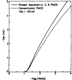
.-. 3 / t 1 I i ~ # " . | I | I 0 I 2 3 -Vgs (Volts)Fig. 3. Comparison of the drain current vs. gate voltage characteris- tics of the rinsed asymmetric Schottky barrier PMOS (solid line) and the conventional PMOS (dashed line) with W/L = 25 I~m/9p~m. The drain voltage is Va, = -O.OSV.
tional PMOS. This is mainly because a m o n g other factors, such as deviation of the threshold voltage and the effective channel length between the two devices, the source sheet resistance of the rinsed asymmetric Schottky barrier P M O S (11 ~/D) is smaller than that of the conventional PMOS (94 ~/D).
Figure 3 shows the Ids-Vgs characteristics of the conven- tional PMOS and the rinsed asymmetric S c h o t t k y barrier P M O S measured at Vds = -0.05V. The gate voltage was s w e p t from 0 to - 5 V . It is seen that the rinsed asymmetric S c h o t t k y barrier PMOS fully recovers the transcon- ductance. The slight difference in slope is mainly due to the difference in source sheet resistance once again.
Figure 4 shows the subthreshold behavior of the conven- tional PMOS and the rinsed asymmetric S c h o t t k y barrier PMOS. Measurements were performed with the drain bi- ased at -0.05 and - 5 V , respectively, on d e v i c e s , w h i c h have a 50 • 25 ~m size of source and drain regions. It is seen that the subthreshold behavior can be fully recovered by the rinsed asymmetric Schottky barrier PMOS because of the e m p l o y m e n t of the conventional drain structure.
10-5
] Rinsed Asymmetric S. B. PMOS
10-'7
//
10-8l I //
10-11 / ~ ' 10-12 " " ~ P ~ ' - ~ Vds = -50 mV 1 0 - TM , I ~ , , i , , , 0.50 0.75 1.00 1.25 1.50 -Vcjs (Volts)Fig. 4. Comparison of subthreshold characteristics of the rinsed asymmetric PMOS (solid line) and the conventional PMOS (dashed line) with W/L = 25 i~m/9 ]~m. The drain is biased at - 5 0 my and -5V, re- spectively.
) unless CC License in place (see abstract).
ecsdl.org/site/terms_use
address. Redistribution subject to ECS terms of use (see
140.113.38.11
J. Electrochem. Soc., Vol. 136, No. 5, May 1989 9 The Electrochemical Society, Inc.
1459
Rinsed Asymmetric S. B. PMO5 . . . . Conventiorml PMO5 0.8
g
- - -O.2 ~
0 10 20 30 40 50 Vds (Volts)Fig. 5. Comparison of breakdown characteristics of the rinsed asym- metric PMOS (solid line) and the conventional PMOS (dashed line) with W/L = 25 I~m/9 I~m.
Comparison of the b r e a k d o w n behavior is shown in Fig. 5. The b r e a k d o w n voltage of the asymmetric S c h o t t k y bar- rier PMOS is comparable to that of the conventional PMOS. It is reasonable to e x p e c t that for the short channel devices, the b r e a k d o w n voltage of the rinsed a s y m m e t r i c S c h o t t k y barrier F M O S would be higher than that of the conventional P M O S due to longer effective channel length at the same mask channel length.
Conclusion
In this work, a novel process for a high-performance modified S c h o t t k y barrier PMOS device was developed.
The process is very simple compared to that of the existing S c h o t t k y barrier PMOS and results in a S c h o t t k y source device without oxide sidewall spacer. The key step, DI water rinse step, was e x a m i n e d in detail and was shown to be reliable and works with less constraint. The a s y m m e t r i c device structure with a P-N j u n c t i o n drain completely re- solves the large subthreshold leakage p r o b l e m associated with the s y m m e t r i c Schottky barrier devices. Thus, the novel process makes the application of the Schottky bar- rier PMOS possible.
Acknowledgment
The authors wish to t h a n k all the staff m e m b e r s of the NCTU.SRC and the financial support furnished by the Na- tional Science Council, China u n d e r Contract no. NSC-76- 0404-E009-10.
Manuscript submitted March 16, 1988; revised manu- script received Aug. 20, 1988.
National Chiao Tung University assisted in meeting the publication costs o f this article.
R E F E R E N C E S
1. P. I. Suciu and R. L. Johnston, IEEE Trans. Electron De- vices, ED-27, 1846 (1980).
2. M. Sugino, L. A. Akers, and M. E. Rebeschini, ibid., ED-30, 110 (1983).
3. S. E. Swirhun, E. Sangiorgi, A. J. Weeks, R. M. Swanson, K. C. Saraswat, and R. W. Dutton, ibid., ED-32, 194 (1985).
4. E. Sangiorgi, M. R. Pinto, S. E. Swirhun, and R. W. Dut- ton, ibid., ED-32, 2117 (1985).
5. C. J. Koeneke, S. M. Sze, R. M. Levin, and E. Kinsbron, IEDM Tech Dig., 367 (1981).
6. C. S. Oh, C. K. Kim, and Y. H. Koh, Proc. Int. VLSI Symp. p. 250, Taipei, China (1985).
7. C. S. Oh, Y. H. Koh, and C. K. Kim, IEDM Tech. Dig., 609 (1984).
LPCVD of Tin Oxide from Tetramethyltin and Oxygen
C. F. W a n , * R. D. McGrath, W . F. Keenan,* and S. N. Frank*
Texas Instruments, Central Research Laboratories, Dallas, Texas 75265
A B S T R A C T
A low-pressure chemical vapor deposition (LPCVD) process using tetramethyltin (TMT) and o x y g e n has been de- v e l o p e d for preparing tin oxide films. Effects of temperature, pressure, and gas flow rates are systematically e x a m i n e d so that the wafer-to-wafer and within-wafer thickness uniformities of less than 5% are obtained in the hotwall L P C V D reac- tor. Twenty-three 75 m m or 100 m m wafers could be deposited during each run. Nominal deposition rate was 55 A/min. Deposition rates as high as 120 A/min was obtained at higher pressure and oxygen flow rates. Characterization results showed that the films were polycrystalline SnO2 with a refractive i n d e x of between 2.00 to 2.10, a visible-light transmission of 84%, and resistivity of 0.6 t2-cm.
Transparent electrode materials find applications in op- toelectronics devices such as solar cells, electrolumines- cent displays, liquid crystal displays, and solid-state imag- ers. With increased process c o m p l e x i t y for advanced optoelectronic devices, good chemical and thermal stabil- ity and mechanical hardness are critical parameters. For example, to directly replace polysilicon gates in a charge- coupled device (CCD), the transparent electrode m u s t un- dergo ion implantation, high-temperature anneal, wafer clean-ups, photoresist strip, H F acid deglaze, SiO2 dry etch, and metallization processes. B o t h polysilicon and tin oxide films m e e t these requirements, but q u a n t u m effi- ciency of the polysilicon-gated CCD is only 35% in the blue region, in contrast to 60% for tin oxide-gated CCDs (1). Var- ious t e c h n i q u e s h a v e b e e n e m p l o y e d to prepare SnO2 films, such as spray hydrolysis, v a c u u m evaporation, reac-
*Electrochemical Society Active Member.
tive R F sputtering, chemical vapor deposition (CVD), and dc glow discharge (2-15). A m o n g these various techniques, L P C V D is c o m m o n l y used for thin film deposition in the fabrication of silicon devices due to its advantages of lower manufacturing cost (15). Thus it is highly desirable to de- velop a L P C V D process for SnO2 that is compatible with present silicon manufacturing technology.
Experimental Technique
A p p a r a t u s . - - T h e deposition is done by direct oxidation of tetramethyltin (TMT) with oxygen in a c o m m e r c i a l hori- zontal hotwall L P C V D system. A schematic of the system is shown in Fig. 1. TMT has a relatively low vapor pressure of 60 m t o r r at 21~ The mass flow controllers (MFC) and gas line were modified so that adequate flow of TMT vapor could be maintained without having to heat the TMT liq- uid source and gas lines. Instead, the TMT was chilled in
) unless CC License in place (see abstract).
ecsdl.org/site/terms_use
address. Redistribution subject to ECS terms of use (see
140.113.38.11