Microstructure and Nonlinear Properties of Microwave-Sintered
ZnO–V
2O
5Varistors: I, Effect of V
2O
5Doping
Cheng-Tzu Kuo, Chang-Shun Chen,
‡and I-Nan Lin
‡Institute of Materials Science and Engineering, National Chiao-Tung University, Hsinchu, Taiwan 300, Republic of China The modification of the densification behavior and the
grain-growth characteristics of the microwave-sintered ZnO materials, caused by the incorporation of V2O5 addi-tives, have been systematically studied. Generally, the ad-dition of V2O5 markedly enhances the densification rate, such that a density as high as 97.9% of the theoretical density and a grain size as large as 10 µm can be attained for a sintering temperature as low as 800°C and a soaking time as short as 10 min. Increasing the sintering tempera-ture or soaking time does not significantly change the sin-tered density of the ZnO–V2O5 materials but it does mo-notonously increase their grain size. Varying the proportion of V2O5in the range of 0.2–1.0 mol% does not pronouncedly modify such behavior. The leakage current density (JL) of these high-density and uniform-granular-structure samples is still large, which is amended by the incorporation of 0.3 mol% of Mn3O4in the ZnO materials, in addition to 0.5 mol% of the V2O5additives. Samples that are obtained using such a method possess good nonohmic characteristics (␣ = 23.5) and a low leakage current density (JL= 2.4 × 10⁻⁶A/cm2).
I. Introduction
Z
INC OXIDE(ZnO) ceramics with several additives are usedas varistor materials, because of their highly nonohmic be-havior in current–voltage (I–V ) characteristics and excellent capability of withstanding surges.1–4 Therefore, these
ZnO-based varistors are extensively used as transient surge sup-pressers against dangerous abnormal high-voltage surges, to protect electronic circuits.5–8It is believed that the nonlinear
I–V characteristics of these materials resulted from the grain-boundary layer, which is essentially formed by a segregation of large ionic additives such as Bi2O3, Pr6O11, and BaO, at the
grain boundary.9–13These ‘‘varistor-forming’’ ingredients
af-fect the electrical properties and the densification behavior and microstructure evolution of ZnO ceramics.
Recently, it was reported that V2O5 is another
varistor-forming ingredient for ZnO ceramics;14–16use of this material
results in varistor properties that are similar to those of ZnO– Bi2O3 ceramics. The advantage of the ZnO–V2O5 system is
that the ceramics can be sintered at relatively low temperature (i.e.,∼900°C) in a conventional electrical furnace. This prop-erty is important for applications of multilayer chip compo-nents, because the material can be cofired with a silver inner
electrode with a melting point of∼961°C. It is expected that the densification behavior can be further improved by using the microwave sintering technique, because it is generally accepted that this process can densify the ceramic materials at a very rapid rate and at a substantially lower temperature.17–20
In this paper, we have made an extensive examination on the effect of sintering temperature and soaking time on the densi-fication behavior of ceramics based on the ZnO–V2O5system.
The correlation between the microstructural characteristics of the materials with their electric properties is discussed.
II. Experimental Procedure
High-purity (>99.9%) ZnO varistor powders, ∼0.8 m in size, were used in the preparations of the ZnO–x-mol%-V2O5
materials (x⳱ 0–1.0). The mixtures with proper compositions were ball-milled in a plastic jar for 8 h, using zirconia balls and deionized water. After the mixtures were filtered and dried, they were calcined at 700°C in air for 2 h, followed by pul-verization in a ball mill for 8 h to a size of∼1.0m and then uniaxially pressed at 750 kgf/cm2into a disk that was 8 mm in
diameter and 2 mm thick. The zirconia contamination was determined, using an inductively coupled plasma (ICP) ana-lyzer, to be <300 ppm. The green pellets,∼60% of the theo-retical density (5.675 g/cm3), were microwave-sintered at
800°–1200°C for 5–60 min in air, using a 2.45 GHz microwave generated from a commercial source (Model GL107 magne-tron, Gerling Co., Modesto, CA). The samples were also
sin-L. M. Levinson—contributing editor
Manuscript No. 191064. Received April 21, 1997; approved February 5, 1998. Supported by the National Science Council of the Republic of China (ROC) through Grant No. NSC 86-2221-E009-041.
†Now with Department of Mechanical Engineering, Hwa-Hsia College of
Tech-nology and Commerce, Taipei, Taiwan 235, ROC.
‡Now with Materials Science Center, National Tsing-Hua University, Hsinchu,
Taiwan 300, ROC.
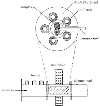
Fig. 1. Schematic drawings of the setup for microwave sintering of ZnO materials.
Journal
tered at 900°–1200°C for 60 min in an electrical furnace to facilitate the comparison. The heating and cooling rates each were 5°C/min.
In the microwave sintering process, the applicator is a seg-ment of a WR284 waveguide (Gerling), schematically shown in Fig. 1, in which a crucible cut from Al2O3 fiberboard is
inserted. The Al2O3fiberboard was selected to reduce the
mi-crowave absorption. SiC rods were used as mimi-crowave absorp-tion susceptors to preheat the samples to∼600°C, because the ZnO pellets can only start to absorb microwave and self-generate the heat at that temperature. The temperature profile was measured using a Pt–13% Rh thermocouple that was placed near the sample surface. The thermocouple, which is shielded, should be oriented perpendicular to the electric field in the waveguide, to minimize the disturbance on the micro-wave and to avoid the arcing caused by the pickup of the electric field. The heating rate was controlled at 60°C/min, and the cooling rate was controlled at 145°C/min for sintering tem-peratures >500°C. The sintering temperature was controlled by adjusting the input microwave power level. The accuracy of the temperature measurement was confirmed by running a test pro-cess, in which TiO2(anatase) samples were heated to∼890°–
910°C. The proportion of phase transformation from anatase to the rutile structure was then compared to the materials that
were heat-treated in an electrical furnace. The temperature measurement was determined to have an accuracy of ±10°C in the setup schematically shown in Fig. 1.
The crystal structure and microstructure of the sintering samples were examined using X-ray diffractometry (XRD) (Model XD-5, Shinadzu Co., Kyoto, Japan) and scanning elec-tron microscopy (SEM) (Model JSM-840A, JEOL, Tokyo, Ja-pan), respectively. The density of the sintered specimens was measured by using the Archimedes method. The average grain size, G, was calculated as described by Mendelson21 with a
multiple factor of 1.56. The I–V properties of these samples were measured by using an electrometer (Model 237 I-V, Keithley Instruments, Cleveland, OH) in a dc source after the indium–gallium (40:60) alloy was rubbed onto the sample sur-face to serve as electrodes. The onset electric field (E0) was
defined as the E-values at a current density of 1.0 mA/cm2, and
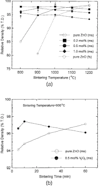
Fig. 2. Densification behavior of ZnO–V2O5materials ((a)
micro-wave-sintered at 800°–1200°C for 10 min (solid curves) or furnace-sintered at 900°–1200°C for 60 min (dotted curve) and (b) microwave-sintered at 900°C for 5–60 min).
Fig. 3. (a) XRD patterns (CuK␣) of ZnO–0.5-mol%-V2O5materials
microwave-sintered at 800°–1200°C for 10 min and (b) EDAX pat-terns of the surface of ZnO–0.5-mol%-V2O5materials samples
micro-wave-sintered either at 900°C (pattern 1, grain interior; pattern 2, grain boundaries) or at 1200°C (pattern 3, grain boundaries).
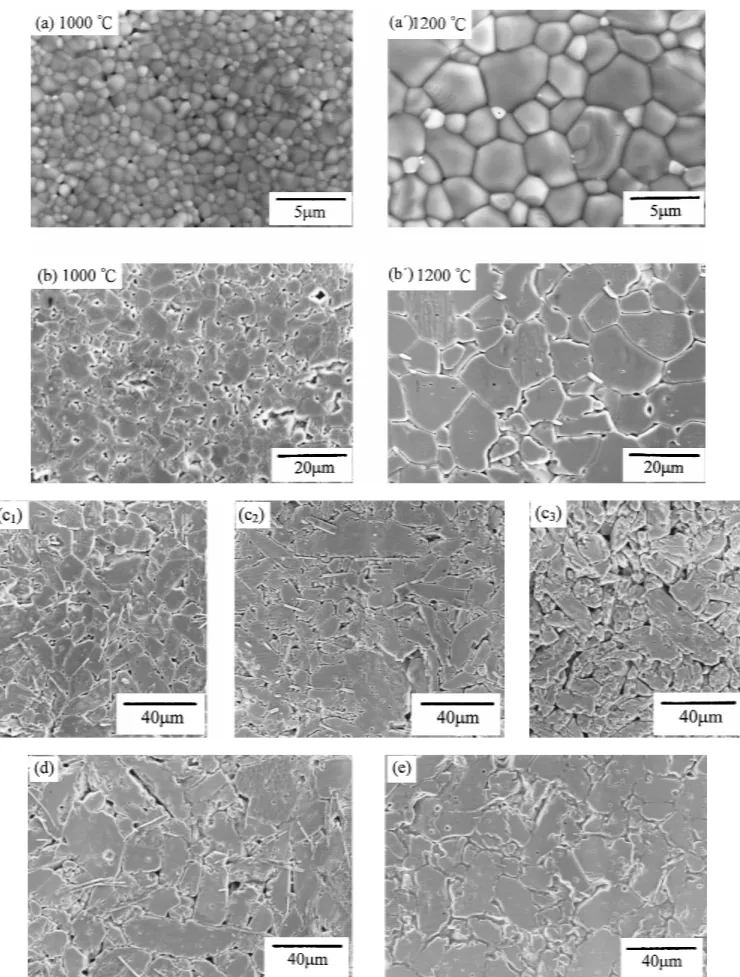
Fig. 4. SEM micrographs of (a and a⬘) the pure ZnO materials densified via the conventional furnace sintering process at 1000° or 1200°C, respectively, for 60 min; (b and b⬘) the pure ZnO materials densified via the microwave sintering process at 1000° or 1200°C, respectively, for 10 min; (c1–c3) ZnO–0.2-mol%-V2O5, ZnO–0.5-mol%-V2O5, and ZnO–1.0-mol%-V2O5materials, respectively, densified via the microwave sintering
process at 900°C for 10 min; (d) ZnO–0.5-mol%-V2O5material densified via the microwave sintering process at 900°C for 60 min; and (e)
the leakage current density (JL) was defined as the J-values at
E–J curves of 10 V/mm. The capacitance–voltage (C–V ) mea-surements were made at room temperature using a capacitance meter (Model HP4274A, Hewlett–Packard, Tokyo, Japan). The electrical characteristics, including barrier height (⌽b) and the
donor density (Nd), were determined from C–V data, using the
model proposed by Mukae et al.22
III. Results and Discussion (1) Sintering Behavior
The beneficial effect of V2O5 on the sintering of the ZnO
ceramics is shown in Fig. 2. The open circles in this figure show that, without the V2O5additives, the ZnO materials can
attain sufficient density (i.e., 94.8% of the theoretical density (TD)) only when they are microwave-sintered at a temperature of >900°C for 10 min. The addition of only 0.2 mol% of V2O5
markedly enhances the densification rate, such that the samples attain a density as high as 97.9% of TD when microwave-sintered at 800°C for 10 min (shown as solid squares in Fig. 2(a)). The samples are hardly densified for sintering tempera-tures <800°C. A density reversion phenomenon—i.e., the
de-crease in density with increasing sintering temperature (Ts)—
occurs for Ts ⱖ 1000°C (marked by arrows). Similar
phenomena are observed for ZnO materials that contain either 0.5 mol% or 1.0 mol% V2O5(shown as solid circles and solid
diamonds, respectively, in Fig. 2(a)). The sintered density of ZnO materials is slightly lower for the samples that contain a larger proportion of V2O5. The temperature of density
rever-sion occurs at 900°C for ZnO–0.5-mol%-V2O5 materials and
800°C for ZnO–1.0-mol%-V2O5materials (marked by arrows
in Fig. 2(a)). For comparison, the densification behavior of pure ZnO materials sintered via the conventional furnace heat-ing process is shown as a dotted line in Fig. 2(a), to indicate that this material requires a higher sintering temperature (i.e., >1000°C) and longer soaking time (i.e., 60 min) to attain a density as high as 94.5% of TD. The advantage of the micro-wave sintering process over the conventional furnace heating process is clearly demonstrated.
The fact that the V2O5 addition can enhance the sintering
behavior of the ZnO materials is further demonstrated by the evolution of the density of the samples with the soaking time. As shown in Fig. 2(b), the density of the pure ZnO materials increases monotonously as the soaking period increases, attain-ing a density of 97.1% of TD when it is microwave-sintered at 900°C for 60 min. However, the ZnO–V2O5materials already
attain a high density (97.4% of TD) when they are microwave-sintered at 900°C for 10 min, and the density of the samples decreases slightly as the soaking time increases thereafter. In other words, the inclusion of V2O5into ZnO materials
mark-edly enhances the densification rate of these materials; how-ever, the density of the samples decreases when the micro-wave-sintering temperature is too high or soak time is too long. To understand how the V2O5modifies the densification of
ZnO materials, the phase constituents of the microwave-sintered ZnO–V2O5materials have been examined. The XRD
patterns in Fig. 3(a) show that the microwave-sintered materi-als consist of a Zn3(VO4)2secondary phase, in addition to the
hexagonal ZnO phase, whereas the energy-dispersive X-ray analyses (EDAX) via SEM on the as-sintered sample surface (patterns 1 and 2 in Fig. 3(b)) show that the vanadium species are mainly located at grain-boundary regions. These results infer that the V2O5enhances the densification of the ZnO
ma-terials via the mechanism of a liquid-phase sintering process. The liquid phase is, presumably, the eutectic phase between ZnO and Zn3(VO4)2. Moreover, EDAX analyses on the 1200°C
microwave-sintered ZnO materials show that no vanadium spe-cies are observable in the grain-boundary regions (pattern 3 in Fig. 3(b)), which clearly indicates the loss of the vanadium species when the sintering temperature is too high. Therefore, the density reversion observed in Figs. 2(a) and (b) can be ascribed to the loss of the volatile vanadium species. This observation agrees with the phenomenon that the density re-version of the high-V2O5-containing materials (i.e., ZnO–1.0
mol% V2O5) occurs at a lower temperature than that for the
ZnO–0.5-mol%-V2O5or ZnO–0.2-mol%-V2O5materials.
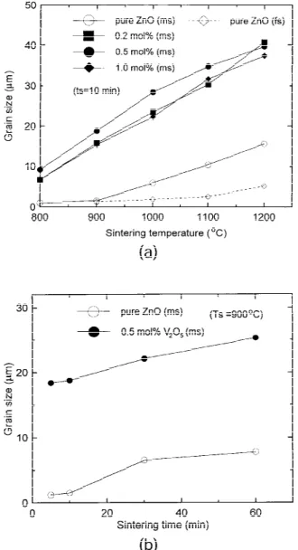
The microwave sintering process increases the densification behavior of ZnO materials and enhances the grain-growth rate of the materials. Figures 4(a) and (a⬘) and Figs. 4(b) and (b⬘) show materials that were formed via conventional furnace sin-tering (fs) and microwave sinsin-tering (ms) processes, respec-tively; these grains of pure ZnO materials have grown monoto-nously as the sintering temperature increases. The grain-growth rate of the ms samples is markedly larger than that of the fs samples, shown as open circles and open diamonds, respec-tively, in Fig. 5(a). The average grain size of the ms samples sintered at 1200°C (10 min), which is ∼12 m, is markedly larger than that of the fs samples sintered at 1200°C (60 min), which is only∼4m.
The addition of the V2O5 species enhances grain growth
even more markedly; however, the proportion of V2O5species
added in ZnO materials does not significantly modify the grain-growth behavior of the samples. Figures 4(c1)–(c3) show that
Fig. 5. Variation of the grain size of the ZnO–V2O5materials with
(a) sintering temperature (microwave-sintered (‘‘ms’’) for 10 min or furnace-sintered (‘‘fs’’) for 60 min) and (b) soaking period (micro-wave-sintered at 900°C).
grains of the ZnO–V2O5materials already grow to a large size
(15–18m) when the material is microwave-sintered at 900°C (10 min), whereas the grains of the pure ZnO materials sintered via the same conditions hardly grow. Moreover, the grain sizes of the samples increase monotonously as the sintering tempera-ture and soaking time increase (Figs. 5(a) and (b), respec-tively). However, the SEM micrographs shown in Figs. 4(d) and (e) indicate that the material still requires a sufficient soak-ing period (i.e., 60 min at 900°C) or an adequate sintersoak-ing temperature (i.e., 1000°C for 10 min) to develop a uniformly large-grained microstructure for ZnO–V2O5materials. Trapped
pores are observed in these samples, which implies that the grain-boundary mobility of the samples has surpassed the drag-ging force of the pores under these sintering conditions. (2) Electrical Properties
The electrical properties of ZnO–V2O5materials are
char-acterized by their E–J behavior. Figures 6(a)–(c) show that the E–J properties are very sensitive to the processing parameters. The leakage of the current density is so pronounced in all the ZnO–V2O5materials that there seems to be no nonlinear
char-acteristics that are observable for all the samples. Figure 6(d) shows that the furnace-sintered samples also possess a large JL
value, except for the 900°C (60 min) sintered samples, which
are ascribed to the insufficient densification of these samples (cf. Fig. 2(a)). Such behavior can be ascribed to the fact that the grain-boundary phase, which is presumably the ZnO–V2O5
compound (i.e., Zn3(VO4)2), reacts with the matrix very well,
which results in an insufficient amount of surface states (Ns)
and a small Schottky barrier height ⌽b along the
grain-boundary regions.
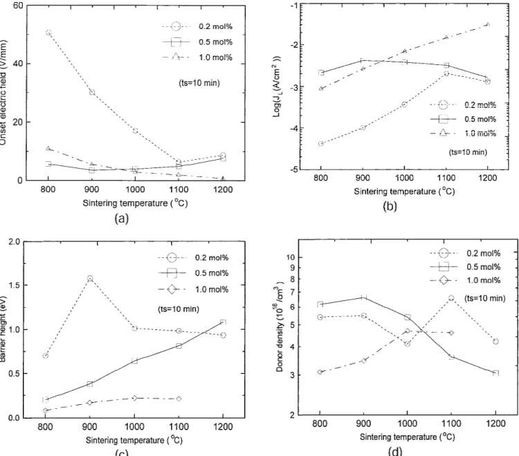
To facilitate the comparison, the onset electric field E0 is
defined as the electric field that corresponds to a current den-sity of 1 mA/cm2 in the E–J curves and the leakage current
density JLis defined as the current density that passes through
the samples under an applied field of 10 V/mm. Figures 6(a)– (c) show that, although the proportion of V2O5 additives
in-cluded in the ZnO materials does not result in significantly different densification and grain-growth behavior of these ma-terials (cf. Figs. 2(a) and 5(a)), it does markedly affect the E–J characteristics of the samples. The sintering temperature de-pendence of E0and JLis shown in Figs. 7(a) and (b),
respec-tively, which indicates that only the ZnO–0.5-mol%-V2O5
ma-terials exhibit more-consistent E0 and JL parameters than the
others; these parameters are E0 ⳱ 3.5–7.6 V/mm and JL ⳱
1.6 × 10⁻³–3.8 × 10⁻³A/cm2.
The fact that the ZnO–0.5-mol%-V2O5 materials possess
much more consistent electric properties is further shown as the Fig. 6. Electric-field–current-density (E–J) characteristics of the (a) ZnO–0.2-mol%-V2O5, (b) ZnO–0.5-mol%-V2O5, and (c)
ZnO–1.0-mol%-V2O5materials microwave-sintered at 800°–1200°C for 10 min; Fig. 6(d) shows the E–J characteristics of the ZnO–0.5-mol%-V2O5materials
sintering-temperature dependence of the barrier height⌽band
the donor density Nd, in the ranges of 0.20–0.81 eV and 3.61 ×
1018–6.60 × 10¹⁸/cm3, respectively (Figs. 7(c) and (d),
respec-tively). Figures 8(a)–(c) indicate again that, for ZnO–0.5-mol%-V2O5materials, the sintering time period (at a sintering
temperature of 900°C) does not significantly alter the E–J char-acteristics and the related electrical parameters (i.e., E0, JL,⌽b,
and Nd), although it moderately changes the sintered density
and the average grain size of the materials (cf. Figs. 2(b) and 5(b)).
The variation of the electrical properties of ZnO–V2O5
ma-terials with the V2O5content can be correlated very well with
the corresponding granular structure. For the materials with a small V2O5content (i.e., ZnO–0.2 mol% V2O5), the granular
structure was fully developed only when they were sintered at sufficiently high temperature. The low-temperature-sintered materials still contain fine grains that are distributed among the large grains; this distribution results in large E0values, which
are accompanied by low apparent JLvalues. On the other hand,
for the materials with a large V2O5 content (i.e., ZnO–1.0
mol% V2O5), high sintering temperatures induced pronounced
V2O5 loss (cf. Fig. 3(b)), which reduces the value of E0 and
increases the value of JL. These results again reveal that the
defect structure along the grain boundaries is another important characteristic that needs to be carefully controlled, in addition to the high sintered density and uniform microstructure, for the purpose of optimizing the electrical behavior of ZnO–V2O5
materials.
As described previously, although the V2O5 addition has
markedly improved the densification and the grain-growth be-havior of the ZnO materials, a substantial leakage current den-sity remained, because of a lack of surface states along the grain boundaries for inducing Schottky barriers in these re-gions. To amend such a discrepancy, 0.3 mol% of Mn3O4was
included into the ZnO materials, in addition to the 0.5 mol% of V2O5, because the manganese species are expected to reside at
the grain-boundary regions and act as electron traps to induce large potential barriers. The bold, solid curve in Fig. 8(a) shows the enormous improvement of the E–J behavior of ZnO mate-rials due to Mn3O4 doping. The leakage current density is
markedly suppressed to JL⳱ 2.4 × 10⁻⁶A /cm2, and the onset
field is pronouncedly increased to E0⳱ 97 V/mm, such that a
nonlinear property with a high nonlinear coefficient (␣ ⳱ 23.5) is achieved. However, the details regarding how the Mn3O4
Fig. 7. Variation of the (a) onset electric field (E0), (b) leakage current density (JL), (c) barrier height (⌽b), and (d) donor density (Nd) of
ZnO–V2O5materials with the sintering temperature.
additives modify the characteristics of ZnO–V2O5 materials
require additional study.
IV. Conclusions
The incorporation of V2O5additives into ZnO materials
pro-nouncedly enhances their densification and grain-growth rates. Densities as high as 97.9% of the theoretical density and grain sizes as large as 10 m can be obtained via microwave sin-tering at temperatures as low as 800°C for 10 min. The sintering temperature and soaking time do not significantly affect the densification rate and the grain-growth behavior; however, they do markedly modify the electrical properties of these materials. The possible interaction between them has been discussed.
References
1M. Inada, ‘‘Crystal Phases on Non-ohmic Zinc Oxide Ceramics,’’ Jpn. J.
Appl. Phys., 17 [1] 1–10 (1978).
2L. M. Levinson and H. R. Philipp, ‘‘Zinc Oxide Varistors—A Review,’’ Am.
Ceram. Soc. Bull., 65 [4] 639–46 (1986).
3T. K. Gupta, ‘‘Application of Zinc Oxide Varistors,’’ J. Am. Ceram. Soc., 73 [7] 1817–40 (1990).
4K. Eda, A. Iga, and M. Matsuoka, ‘‘Degradation Mechanism of Non-ohmic Zinc Oxide Ceramics,’’ J. Appl. Phys., 51 [5] 2678–84 (1980).
5J. Erickson and B. Reich, ‘‘The High Power Metal-Oxide Varistor as a Vehicle and Aircraft Transient Suppresser,’’ IEEE Trans. Aerosp. Electron.
Syst., AES–12, 104–108 (1976).
6L. M. Levinson and H. R. Philipp, ‘‘ZnO Varistors for Transient Protec-tion,’’ IEEE Trans. Parts, Hybrids, Packag., PHP–13, 338–43 (1977).
7E. C. Sakshaug, J. S. Kresge, and S. A. Miske, ‘‘A New Concept in Station Arrestor Designs,’’ IEEE Trans. Power Appar. Syst., PAS-96, 647–56 (1977). 8R. Einzinger, ‘‘Metal Oxide Varistors,’’ Annu. Rev. Mater. Sci., 17, 299–321 (1987).
9M. Matsuoka, ‘‘Nonohmic Properties of Zinc Oxide Ceramics,’’ Jpn. J.
Appl. Phys., 10 [6] 736–46 (1972).
10K. Mukae, K. Tsuda, and I. Nagasawa, ‘‘Non-Ohmic Properties of ZnO– Rare Earth Metal Oxide–Co3O4Ceramics,’’ Jpn. J. Appl. Phys., 16 [8] 1361–68 (1977).
11Y.-S. Lee and T.-Y. Tseng, ‘‘Phase Identification and Electrical Properties in ZnO–Glass Varistors,’’ J. Am. Ceram. Soc., 75 [6] 1636–40 (1992).
12K. Uematsu, A. Terada, T. Morimoto, N. Uchida, and K. Saito, ‘‘Direct Determination of Grain Growth Behavior in Zinc Oxide with Added Barium Oxide,’’ J. Am. Ceram. Soc., 72 [6] 1070–72 (1989).
13T. R. N. Kutty and N. Raghu, ‘‘ZnO-Based Voltage-Limiting Resistors with MCoO3−x(M≡Ba, Sr) as the Only Forming Additives,’’ Mater. Sci. Eng.,
B, B13, 181–97 (1992).
14G. Calestani, L. Marshignani, and A. Montenero, ‘‘DC Conductivity of ZnO–V2O5Glasses,’’ J. Non-Cryst. Solids, 86, 285–92 (1986).
15J. K. Tsai and T. B. Wu, ‘‘Non-Ohmic Characteristics of ZnO–V 2O5 Ce-ramics,’’ J. Appl. Phys., 76 [8] 4817–22 (1994).
16J. K. Tsai and T. B. Wu, ‘‘Microstructures and Nonohmic Properties of ZnO–V2O5Ceramics,’’ Jpn. J. Appl. Phys., 34 [12] 6452–57 (1995).
17W. H. Sutton, ‘‘Microwave Processing of Ceramic Materials,’’ Am. Ceram.
Soc. Bull., 68 [2] 376–86 (1989).
18M. A. Janney, C. L. Calhoum, and H. D. Kimery, ‘‘Microwave Sintering of Solid Oxide Fuel Cell Materials: I. Zirconia–8 mol% Yttria,’’ J. Am. Ceram.
Soc., 75 [2] 341–46 (1992).
19H. Y. Chang, K. S. Liu, and I. N. Lin, ‘‘Electrical Characteristics of (Sr0.2Ba0.8)TiO3 Positive Temperature Coefficient of Resistivity Ma-terials Prepared by Microwave Sintering,’’ J. Appl. Phys., 77 [11] 1–5 (1995).
20C. S. Chen, C. T. Kuo, and I. N. Lin, ‘‘Electrical Properties of ZnO Varis-tors Prepared by Microwave Sintering Process,’’ Jpn. J. Appl. Phys., 35 [9] 4696–703 (1996).
21M. I. Mendelson, ‘‘Average Grain Size in Polycrystalline Ceramics,’’ J.
Am. Ceram. Soc., 52 [8] 443–46 (1969).
22K. Mukae, K. Tsuda, and I. Nagasawa, ‘‘Capacitance-vs-Voltage Charac-teristics of ZnO Varistors,’’ J. Appl. Phys., 50 [6] 4475–76 (1979). 䊐 Fig. 8. Variation of (a) the E–J characteristics, (b) the onset electric
field (E0) and the leakage current density (JL), and (c) the barrier
height (⌽b) and donor density (Nd) with the soaking time (5–60 min)
of the ZnO–0.5-mol%-V2O5 (Z-0.5V-0M) materials
microwave-sintered at 900°C (the bold curve in Fig. 8(a) shows the modification on the E–J curve due to the Mn3O4addition, Z-0.5V-0.3M).