Monitoring the 3D Nanostructures of Bulk
Heterojunction Polymer Solar Cells Using Confocal
Lifetime Imaging
Jen-Hsien Huang,†Fan-Ching Chien,†Peilin Chen,*,†Kuo-Chuan Ho,*,‡,§and Chih-Wei Chu*,†,⊥
Research Center for Applied Sciences, Academia Sinica, Taipei, Taiwan 115, Department of Chemical Engineering and Institute of Polymer Science and Engineering, National Taiwan University, Taipei, Taiwan 10617, and Department of Photonics, National Chiao Tung University, Hsinchu, Taiwan
In this study, the exciton lifetime images within the photoactive layers of poly(3-hexylthiophene) (P3HT) and [6,6]-phenyl-C61-butyric acid methyl ester (PCBM) are revealed by confocal optical microscopy combined with the fluorescence module. The images reveal that the active layers during slow solvent evaporation provide 3D path-ways for charge transport and the concentration gradient through the film which reflects the better cell perfor-mance. This technique offers a great help to investigate the 3D optical-physical property without destroying the blends.
We face an energy crisis in which the demand for available energy grows with each passing day; therefore, finding alternative forms of renewable energy is becoming a critical issue. Heeger et al. first proposed the concept of bulk heterojunction (BHJ) solar cells by blending poly[2-methoxy-5-(3,7-dimethyloctyloxy)]-1,4-phenylenevinylene (MDMO-PPV) as the electron donor with [6,6]-phenyl-C61-butyric acid methyl ester (PCBM) as the electron acceptor; since then, BHJ solar cells have become the subject of intense research activity.1 The main feature of BHJ solar cells is the significantly increased interfacial surface area between the donor and acceptor, allowing more efficient charge separation relative to that in the planar interface of bilayer cells. Nevertheless, the power conversion efficiencies (PCEs) of solar cell devices remain limited by unfavorable morphologies at their interfacial areas, leading to poor charge transport within the blends. Because recombination should be prevented prior to the carriers reaching the electrodes, the ideal morphology would combine a large donor-acceptor interfacial area and continuous channels for the holes and electrons to travel to their respective electrodes. Therefore, an efficient polymer solar cell should feature a suitable 3D acceptor-donor network within its blend film.
Several morphological advances in polymer-based solar cells have been demonstrated to enhance the PCE.2-9Among these techniques, the most remarkable breakthrough has been the enhancement in polymer chain crystallinity through either thermal or solvent annealing. After annealing, holes can be transported directly through the polymer channel as a result of the formation of an interpenetration network within the blend film. Another important method developed recently is the addition of al-kanedithiols into the solvent used to fabricate the solar cell devices.10-14These alkanedithiols selectively dissolve PCBM but not poly(3-hexylthiophene) (P3HT) or any of the other polymers used. This approach allows efficient phase separation to occur during the drying process, leading to a favorable morphology. Although scanning electron microscopy (SEM), transmission electron microscopy (TEM), atomic force microscopy (AFM), scanning electrical potential microscopy (SEPM),15 and X-ray photoelectron spectroscopy (XPS)16,17 are excellent tools for monitoring the lateral morphologies and chemical composition of blend films, it is difficult to examine their vertical morphologies and distributions of components using these techniques.
* Corresponding author. E-mail: [email protected] (P.C.); kcho@ ntu.edu.tw (K.-C.H.); [email protected] (C.-W.C.). Telephone: 886-2-27898000ext 33 (P.C.); +886-2-23660739 (K.-C.H.); +886-2-886-2-27898000ext 70 (C.-W.C.). Fax: 886-2-27826680 (P.C.); +886-2-23623040 (K.-C.H.); +886-2-27826680 (C.-W.C.).
†
Research Center for Applied Sciences, Academia Sinica.
‡Department of Chemical Engineering, National Taiwan University. §
Institute of Polymer Science and Engineering, National Taiwan University.
⊥Department of Photonics, National Chiao Tung University.
(1) Yu, G.; Gao, J.; Hummelen, J. C.; Wudl, F.; Heeger, A. J. Science 1995,
270, 1789–1791.
(2) Padinger, F.; Rittberger, R. S.; Sariciftci, N. S. Adv. Funct. Mater. 2003,
13, 85–88.
(3) Li, G.; Shrotriya, V.; Yao, Y.; Yang, Y. J. Appl. Phys. 2005, 98, 043704-1– 043704-5.
(4) Ma, W.; Yang, C.; Gong, X.; Lee, K.; Heeger, A. J. Adv. Funct. Mater. 2005,
15, 1617–1622.
(5) Li, G.; Shrotriya, V.; Huang, J.; Yao, Y.; Moriarty, T.; Emery, K.; Yang, Y.
Nat. Mater.2005, 4, 864–868.
(6) Shrotriya, V.; Yao, Y.; Li, G.; Yang, Y. Appl. Phys. Lett. 2006, 89, 063505-1–063505-3.
(7) Li, G.; Yao, Y.; Yang, H.; Shrotriya, V.; Yang, G.; Yang, Y. Adv. Funct. Mater. 2007, 17, 1636–1644.
(8) Chen, H. Y.; Yang, H.; Yang, G.; Sista, S.; Zadoyan, R.; Li, G.; Yang, Y. J.
Phys. Chem. C2009, 113, 7946–7953.
(9) Yao, Y.; Hou, J.; Xu, Z.; Li, G.; Yang, Y. Adv. Funct. Mater. 2008, 18, 1783– 1789.
(10) Peet, J.; Kim, J. Y.; Coates, N. E.; Ma, W. L.; Moses, D.; Heeger, A. J.; Bazan, G. C. Nat. Mater. 2007, 6, 497–500.
(11) Lee, J. K.; Ma, W. L.; Brabec, C. J.; Yuen, J.; Moon, J. S.; Kim, J. Y.; Lee, K.; Bazan, G. C.; Heeger, A. J. J. Am. Chem. Soc. 2008, 130, 3619–3623. (12) Monson, T. C.; Lloyd, M. T.; Olson, D. C.; Lee, Y. J.; Hsu, J. W. P. Adv.
Mater.2008, 20, 4755–4759.
(13) Pivrikas, A.; Stadler, P.; Neugebauer, H.; Sariciftci, N. S. Org. Electron. 2008, 9, 775–782.
(14) Cho, S.; Lee, J. K.; Moon, J. S.; Yuen, J.; Lee, K.; Heeger, A. J. Org. Electron. 2008, 9, 1107–1111.
(15) Yu, B. Y.; Lin, W. C.; Huang, J. H.; Chu, C. W.; Lin, Y. C.; Kuo, C. H.; Lee, S. H.; Wong, K. T.; Ho, K. C.; Shyue, J. J. Anal. Chem. 2009, 81, 8936– 8941.
Anal. Chem. 2010, 82, 1669–1673
Ingana¨s et al. recently employed electron tomography (ET) to reconstruct a 3D image of the BHJ blends from series 2D projections; this approach provides a great deal of structural information.18Heeger et al. used TEM to analyze thin slices of the BHJ film, observing the columnlike structures that provided the pathways for charge transport.19Loos et al. used ET and TEM to investigate the morphologies within blend films, from which they constructed 3D images.20,21Yang et al. successfully applied XPS to analyze the vertical composition profiles of BHJ films.22 Although these approaches have all offered detailed information regarding the morphologies and compositions within blend films, no attention has been focused previously on the films’ 2D and 3D opticophysical properties, even though they are the most fundamental characteristics directly influencing cell performance. With the aim of understanding the complete morphology of the exciton lifetime, in this study, we performed a comprehensive analysis of the 2D nanoscale morphology related to the exciton lifetime by combining confocal optical microscopy with a fluores-cence module. This approach provides much fundamental infor-mation that is unavailable when conventional microscopy tech-niques are used.
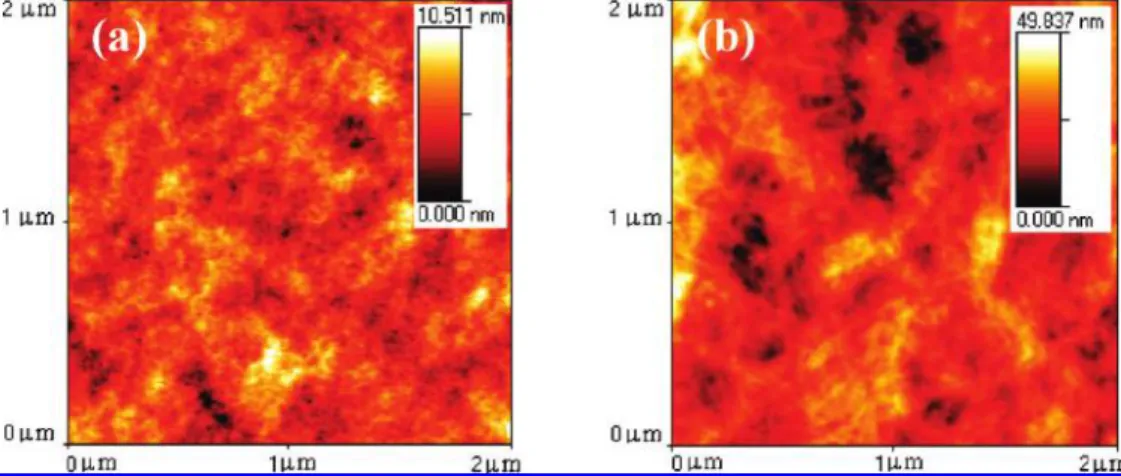
To examine the effect of the morphology on the exciton lifetime under realistic device conditions, we prepared BHJ films based on P3HT and PCBM, with and without solvent annealing. Figure 1 presents AFM images comparing the surface morphologies of the films spin-cast onto indium tin oxide (ITO) substrates. The rapidly grown film exhibits an even and featureless morphology (Figure 1a), whereas the slowly grown film presents thin, chainlike features running across its surface (Figure 1b). These features originated from domains of P3HT crystallites, which contain several tightly packed polymer chains. Even though it is believed
that such chainlike features arising from the stacking of P3HT units enhance charge transport, detailed information regarding electron/hole dissociation and the exciton lifetime within the film is unavailable.
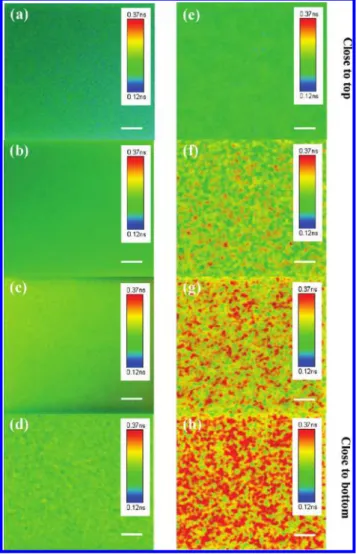
It is well-known that the depth z-resolution of confocal optical microscopy depends on the laser wavelength applied which is about 400-500 nm. In order to gain the detailed information of the exciton lifetime along the z-axial, we prepare thick films with a thickness of 2 µm via drop coating, allowing us to reconstruct a 3D lifetime image of BHJ blends. Figure 2 displays the exciton lifetime images of BHJ films prepared from rapidly and slowly grown methods. These thick films were measured as four layers with an interval of 500 nm. These data provide information hidden from the surface examination in Figure 1. The exciton lifetime images of the rapidly grown films reveal an extremely homoge-neous lifetime distribution. Although significant photolumines-cence (PL) quenching while blending P3HT and PCBM provided much electron/hole pair dissociation, the uniform phase could not provide bicontinuous transport pathways for holes and electrons, resulting in a decrease of photocurrent. Notably, although the BHJ film possessed a phase exhibiting well-mixed features, the overall exciton lifetime decreased gradually from the bottom to the top. This behavior indicates that the P3HT concentration on the PEDOT:PSS side of the films was much higher than that at the top surface; therefore, a vertical concentra-tion gradient existed within the film. This finding suggests that an inhomogeneous P3HT distribution in spin-coated films is favorable because an ITO substrate coated with PEDOT:PSS is used as the anode in regular devices. It has been shown that the vertical composition gradient of P3HT and PCBM significantly enhances the electron blocking ability of PEDOT:PSS, the ef-ficiency of photoinduced electron transfer and the photocurrent of the device.23,24Additionally, the vertical composition gradient also can balance the electron and hole mobility, resulting in a decrease of series resistance. These are entirely positive effects in terms of solar cell efficiency. Although the concentration gradient favors a balanced charge mobility between electrons and holes, bicontinuous transport pathways continued to dominate the overall charge transport in the rapidly grown films. In the case of (16) Yu, B. Y.; Chen, Y. Y.; Wang, W. B.; Hsu, M. F.; Tsai, S. P.; Lin, W. C.; Lin,
Y. C.; Jou, J. H.; Chu, C. W.; Shyue, J. J. Anal. Chem. 2008, 80, 3412– 3415.
(17) Chen, Y. Y.; Yu, B. Y.; Wang, W. B.; Hsu, M. F.; Lin, W. C.; Lin, Y. C.; Jou, J. H.; Shyue, J. J. Anal. Chem. 2008, 80, 501–505.
(18) Andersson, B. V.; Herland, A.; Masich, S.; Ingana¨s, O. Nano Lett. 2009, 9, 853–855.
(19) Moon, J. S.; Lee, J. K.; Cho, S.; Byun, J.; Heeger, A. J. Nano Lett. 2009, 9, 230–234.
(20) van Bavel, S. S.; Sourty, E.; de With, G.; Loos, J. Nano Lett. 2009, 9, 507– 513.
(21) van Bavel, S.; Sourty, E.; de With, G.; Veenstrabd, S.; Loos, J. J. Mater.
Chem.2009, 19, 5388–5393.
(22) Xu, Z.; Chen, L. M.; Yang, G.; Huang, C. H.; Hou, J.; Wu, Y.; Li, G.; Hsu, C. S.; Yang, Y. Adv. Funct. Mater. 2009, 19, 1–8.
(23) Kumar, A.; Li, G.; Hong, Z.; Yang, Y. Nanotechnology 2009, 20, 165202– 165205.
(24) Sun, Q.; Park, K.; Dai, L. J. Phys. Chem. C 2009, 113, 7892–7897.
slowly grown film, the images of the exciton lifetime reveal a significantly different behavior relative to that of the films prepared without solvent annealing (Figures 2e-h). We assign the long (red regions) and short (green regions) lifetime domains to the P3HT- and PCBM-rich domains, respectively. The exciton lifetime ranges from 0.37 to 0.12 ns for P3HT- and PCBM-rich domains. A slow rate of solvent evaporation facilitates the growth of highly crystalline P3HT; therefore, a portion of the PCBM molecules were gradually expelled from the P3HT domains during the formation of crystalline P3HT, resulting in the formation of P3HT-and PCBM-rich domains. The images clearly reveal that some domains were continuous from the bottom to the top, forming percolating pathways, but others were discontinuous. Further-more, we calculated the charge mobility in the BHJ films from the space-charge limited current (SCLC),25using the equation
J )9ε0εrµV2/8L3
where ε0εris the permittivity of the polymer, µ is the carrier mobility, and L is the device thickness. For the rapidly grown
film, the electron and hole mobilities were 4.3× 10⁻⁸and 1.2 × 10⁻⁹m2V-1s-1, respectively. For the slowly grown film, the electron and hole mobilities both increased to 1.9× 10⁻⁷and 1.3× 10⁻⁷ m2 V-1s-1, respectively. Because the ratio of the electron and hole mobilities was close to 1.46, we infer that the bicontinuous transport pathways within the entire active layer not only enhanced the charge transport but also balanced the mobility. Moreover, the P3HT-rich domains (red regions) decreased in size gradually from the bottom to the top, suggesting that a concentration gradient also existed in the slowly grown films.
Figure 3 displays the average values of the exciton lifetimes for both the rapidly and slowly grown films, from the bottom to the top layer. We quantified these data from the distribution of the lifetime in the vertical position (error bars were produced by measuring 10 different positions for each layer). The inset to Figure 3 presents the lifetime distribution for the bottom layer of the slowly grown film. The distribution of the measured lifetime values followed Gaussian functions in all cases. Both the rapidly and slowly grown films exhibited an increase in the concentration of PCBM upon progressing from the bottom layer to the top. The plot for the slowly grown film, however, featured a larger slope relative to that of the rapidly grown film. The vertical concentration gradient in the BHJ films arose as a result of differences in the surface energies of each component. Because P3HT has a lower surface energy than PCBM, it tends to accumulate at the PEDOT: PSS side to minimize the Gibbs free energy.26,27The slowly grown film was formed over a sufficient length of time for the morphol-ogy to achieve thermodynamic equilibrium during the solvent evaporation process. In contrast, the rapidly grown film did not attain a thermodynamically favorable morphology because of its shorter growth time; as a result, it featured a smaller concentration gradient than that of the slowly grown film. Loos et al. observed similar phenomena in other polymer blend systems.20,21
(25) Gill, W. D. J. Appl. Phys. 1972, 43, 5033–5040.
(26) Bjo¨rstro¨m, C. M.; Bernasik, A.; Rysz, J.; Budkowski, A.; Nilsson, S.; Svensson, M.; Andersson, M. R.; Magnusson, K. O.; Moons, E. J. Phys.:
Condens. Matter.2005, 17, L529–L534.
(27) Heriot, S. Y.; Jones, R. A. L. Nat. Mater. 2005, 4, 782–786.
Figure 2. (a-d) Exciton lifetime images of the rapidly grown BHJ
film and (e-h) exciton lifetime images of the slowly grown BHJ film prepared via drop coating, from the bottom layer to the top, measured after excitation at 470 nm using a picosecond laser microscope (512 × 512 pixels). Scale bars: 2 µm.
Figure 3. Average values of the experimentally measured exciton
lifetimes of the rapidly and slowly grown P3HT:PCBM films. Inset: Distribution of exciton lifetimes of the slowly grown P3HT:PCBM film (bottom layer).
In order to investigate the exciton lifetime distribution under a real device condition, we also prepare thin BHJ films with the same thickness as our devices (∼200 nm). Figure 4 reveals the transmitted and exciton lifetime images of thin BHJ films. The transmitted image of the rapidly grown film (Figure 4a) display uniform and featureless characteristics throughout the structure, indicating that P3HT and PCBM were mixed well within the films. This monotonous transmitted image is responsible for the uniform lifetime distribution which is in good agreement with the results obtained from thick films. Figure 4c-d displays transmitted and exciton lifetime images for the slowly grown films. The transmitted image reveals many emissive spots. The bright spots are emissions from many polymer chains that have stacked or aggregated into a bulk cluster; they maintain a certain level of PL intensity because the aggregation of polymer chains expels some PCBM molecules from the P3HT domain, leading to a lower level of PL quenching. These images also reveal the presence of dark areas in other regions, meaning that the emission was quenched through ultrafast photoinduced charge transfer from P3HT to PCBM. When the exiton lifetime image (Figure 4d) was carefully observed, it revealed that the red regions (P3HT-rich domains) corresponded to the bright spot of the transmitted image (Figure 4c) and the lifetime images were almost the same in the thick and thin films. From these results, we can conclude that thick and thin films follow the same film growth behavior. Therefore, we consider the percolating pathways also exist in the case of thin films.
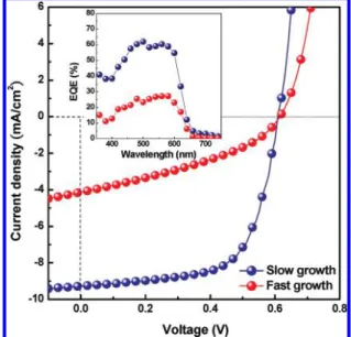
Figure 5 displays the J-V characteristics and external quantum efficiencies (EQEs) of photovoltaic devices incorporating the rapidly and slowly grown films. The short-circuit current (JSC) and fill factor (FF) of the device fabricated using solvent annealing were 9.3 mA cm-2and 66%, respectively. These values are both much higher than those exhibited by the rapidly grown film (JSC) 4.1 mA cm-2; FF ) 38%). The maximum EQE for the device prepared with the rapidly grown film was 27.2% at a wavelength of 560 nm. In contrast, for the device incorporating the slowly grown film, the EQE maximum increased to ca. 62% at 500 nm. This increase in EQE within this wavelength range contributed to the increase in the values of JSCof the devices.
When a bicontinuous transport pathway is formed within a BHJ film, the carrier can be transported to the electrode more readily, leading to a larger value of JSC. In addition, we suspect that the larger vertical concentration and balanced carrier mobility resulted in the enhanced FF.
Taking all of our results into consideration, Scheme 1 presents schematic representations of the proposed vertical morphologies in the rapidly and slowly grown films. The lower surface energy of P3HT, relative to PCBM, provides the driving force for the interconcentration gradient that we observed in both the rapidly and slowly grown films. The film prepared through a rapidly grown process leads to an extremely homogeneous blend as shown in Scheme 1a. A homogeneous phase cannot offer a continuous pathway for charge transport, leading to a serious recombination which can be radiative or nonradiative in nature and can release energy via photoluminescence. A greater number of percolating pathways were formed across the slowly grown film as shown in Scheme 1b. Although not all of these pathways may have been ideal, due to the presence of some terminated channels, this system still offered several connected pathways, leading to an interdigitated nanostructure that was responsible for efficient charge transport and the superior value of JSC.
In conclusion, we have combined confocal optical microscopy with a fluorescence module to study the opticophysical properties
Figure 4. (a, c) Transmitted images and (b, d) exciton lifetime images
of the BHJ film prepared from rapidly and slowly grown methods, respectively, measured after excitation at 470 nm using a picosecond
laser microscope (512× 512 pixels). Scale bars: 2 µm. Figure 5. J-V characteristics under illumination at 100 mW cm-2
(simulated AM 1.5G) of photovoltaic devices incorporating active layers prepared at two different growth rates. Inset: EQE spectra of the devices incorporating the rapidly and slowly grown films.
Scheme 1. Schematic Representation of the Vertical Phase Morphology of the (a) Rapidly and (b) Slowly Grown P3HT:PCBM Blend
within P3HT:PCBM films. This approach allowed us to investigate the exciton lifetime distribution within the films under realistic device conditions. Detailed analysis revealed that the solvent evaporation rate could control the number of percolating pathways and the slope of the vertical concentration gradients. This powerful technique allows the direct and simple study of the relationship between the fabrication conditions and the vertical film morphology.
EXPERIMENTAL SECTION
Device Fabrication. The polymer photovoltaic devices were
fabricated by spin-coating a blend of P3HT:PCBM onto a poly-(ethylene dioxythiophene)/polystyrenesulfonate (PEDOT:PSS)-modified ITO surface. Prior to deposition, the P3HT:PCBM blend was dissolved in 1,2-dichlorobenzene at a 1:1 weight ratio. The active layer was obtained by spin-coating the blend at 600 rpm for 60 s. The active layer was then dried in a covered glass Petri dish. Next, 30 and 100 nm thick layers of Ca and Al, respectively, were thermally evaporated under vacuum at pressures of less than 6 × 10⁻⁶ torr. In the hole-only devices, we replaced Ca with MoO3because its higher work function (Φ ) 5.3 eV) provided a better hole injection contact for P3HT:PCBM.27The layer of MoO3was thermally evaporated to a thickness of 20 nm, and then, it was capped with a 50 nm layer of Al. For the electron-only devices, we replaced the PEDOT:PSS layer with CsCO3 (Φ ) 2.9 eV), which has been used previously as an efficient electron injection layer.28,29This layer of Cs
2CO3was thermally evaporated to a thickness of 2 nm. The active layers were then
annealed at 130 °C for 20 min to provide the final hole- and electron-only devices.
Characterization. We tested the cell performance under
simulated AM 1.5G irradiation at 100 mW cm-2using a Xe lamp-based solar simulator (Thermal Oriel 1000W). The light intensity was calibrated using a monosilicon photodiode equipped with a Hamamatsu KG-5 color filter. The whole measurement process was performed at room temperature in a glovebox filled with N2. The surface morphologies of the polymer films were investigated using AFM (Digital Instrument NS 3a controller equipped with a D3100 stage). The samples were excited with light having a wavelength of 470 nm from a picosecond laser (LDH-P-C-470, PicoQuant); the fluorescence lifetime signal was measured using time-correlated single photon counting (TCSPC). The samples were scanned using an Olympus FV300 confocal optical microscope equipped with a PicoQuant PDM single photon avalanche diode detector and a PicoQuant PicoHarp 300 USB interface for time-correlated single photon counting to map the lifetime image. The fluorescence signal was improved using an edge filter (REF-473.0-25, CVI). The acquisition time for each lifetime image (pixel size: 512× 512) was 20 min.
ACKNOWLEDGMENT
J.-H.H. and F.-C.C. contributed equally to this work. The authors are also grateful to the National Science Council (NSC), Taiwan, (NSC 97-2120-M-002-012 and NSC 96-2628-E-007-030-MY2) and Academia Sinica, Taiwan for financial support.
Received for review September 4, 2009. Accepted January 17, 2010.
AC901992C
(28) Shrotriya, V.; Li, G.; Yao, Y.; Chu, C. W.; Yang, Y. Appl. Phys. Lett. 2006,
88, 073508-1–073508-3.
(29) Shrotriya, V.; Yao, Y.; Li, G.; Yang, Y Appl. Phys. Lett. 2006, 89, 063505-1–063505-3.