Department of Applied Chemistry and Institute of Molecular Science, College of Science, National Chiao Tung University, 1001 Ta-Hsueh Road, Hsinchu 30010, Taiwan
§Graduate School of Materials Science, Nara Institute of Science and Technology, 8916-5 Takayama, Ikoma, Nara 630-0192, Japan ∥Advanced Technology Research Laboratories, Panasonic Corporation, Seika, Kyoto 619-0237, Japan
*
S Supporting InformationABSTRACT: The first six peptides of multifunctional
titanium binding peptide-1 bestowed recombinant L-ferritin, minT1-LF, was genetically engineered and used to fabricate multilayered nanoparticle architecture. The multifunctionality of minT1-LF enables specific binding of nanoparticle-accommodated minT1-LF to the silicon substrate surface and wet biochemical fabrication of gate oxide layer by its biomineralization activity. Three-dimensional (3D) nano-particle architecture with multilayered structure was fabricated by the biological layer-by-layer method and embedded in a
metal oxide−semiconductor device structure as a charge storage node of a flash memory device. The 3D-integrated multilayered nanoparticle architecture successfully worked as a charge storage node inflash memory devices that exhibited improved charge storage capacity compared with that of a conventional monolayer structure device.
C
ontrolled fabrication of three-dimensional (3D) arrays of bioinorganic hybrid materials using the ability of biomolecules to biomineralize is drawing considerable attention because of its potential to produce hierarchical structures for nanoelectronics and surface architectures for sensing devices and structural analysis. Hybrid bioinorganic matrices that are generated using a 3D protein template array encapsulated with biomineralized inorganic material allow versatile use of the inherent functionality of biomaterials for different applications.1Targeting of specific materials is one such functionality of biomaterials. Peptide aptamers that target inorganic materials have inspired remarkable advances in engineering during the past decade, particularly with bottom-up fabrication at the nanometer scale.2 The goal of biofunctionality-assisted fabrication is the self-organization of nanoscale building blocks to allow downsizing of large-scale integration (LSI) technol-ogy.3−5 The sophisticated ability of biomolecules to self-organize in the nanometer regime has encouraged us to fabricate hierarchical nanoarchitectures using the automated molecular interactions of functional biomolecules.6−8
Peptide evolution systems have played an important role in the effort to realize this goal because they use a number of target inorganic materials that can be specifically recognized by biomolecules.9,10 We previously reported isolation of peptide aptamer titanium binding peptide-1 (TBP-1) that discriminates and binds to the surface of specific materials.11,12For example,
TBP-1 selectively recognizes and binds to Ti, Ag, and Si surfaces, but not to those of Au, Cr, Pt, Sn, Zn, Cu, or Fe. TBP-1 also promotes mineralization of titanium oxide (titania), silicon oxide (silica), and Ag.12,13Thus, TBP-1 is a bifunctional peptide, as is often the case for peptide aptamers that target inorganic materials. Although TBP-1 is composed of 12 amino acids, it has been revealed that the first hexapeptide in the sequence, Arg-Lys-Leu-Pro-Asp-Ala, mediates specific binding and the mineralization function of this peptide aptamer.11We have named this hexapeptide aptamer “minTBP-1”. The bifunctionality of minTBP-1 can be endowed on other molecules both by genetic and chemical display at their N-terminals.14−16We equipped a protein with the bifunctionality of minTBP-1 by addition of the peptide aptamer to a protein molecule by making a recombinant protein, minT1-LF [Figure S1, Supporting Information (SI)]. This protein possesses genetically displayed minTBP-1 on the surface of recombinant L-ferritin molecules. MinT1-LF showed a greater affinity for target silica and drastically lowered the necessary protein concentration for silica mineralization compared with original minTBP-1 peptide.14,16 The biomineralization function of the aptamer enabled a novel method to produce multilayered
Received: July 21, 2013 Revised: September 11, 2013 Published: September 12, 2013
protein−inorganic nanoparticle architectures by biomimetic layer-by-layer assembly (BioLBL) to be developed.16BioLBL alternately utilizes the binding and silicification capabilities of minT1-LF to assemble multilayered nanostructures composed of layers of minT1-LF and intercalating silica. In addition, we have established the X−Y positioning of mutant ferritin displaying a peptide aptamer and controlled stacking in the Z-dimension through the specific binding of minT1-LF and BioLBL.13
Ferritin is a cage-shaped protein with an interior space of 7− 8 nm.17It is able to accommodate a wide variety of inorganic nanoparticles including hydrated and oxidized metals and
semiconductors via biomineralization.18−20 MinT1-LF also showed the ability to incorporate ferrihydrite, cobalt oxide, and cadmium selenide into its interior space via biomineraliza-tion.16Multiple layers of inorganic nanoparticles separated by intervening layers of ferritin can be constructed by BioLBL. The mineral layer between protein layers prevents interlayer diffusion of minT1-LF, and nanoparticles in ferritin cages are aligned in the layer adjacent to the substrate with the same density. Fabrication of such alternating nanometer-scaled layered structures is difficult to achieve using conventional layer-by-layer methods because of interlayer diffusion.16 The satisfactory layer control of BioLBL allows us to fabricate
Figure 1.Schematic diagram of the BioLBL process used to fabricate MOS-basedflash memory devices. The first monolayer of Fe@minT1-LF is formed on the cleaned silicon substrate. A silica layer is deposited on top of the layer of minT1-LF via mineralization mediated by minTBP-1. The newly formed silica layer then serves as a binding target for a second Fe@minT1-LF layer. By repeating these binding and mineralization cycles, multilayered structures are fabricated. Following this BioLBL process, ferritin shells were removed by UV oxidation. After the layers of Fe-BNDs were embedded in a control gate layer by plasma CVD, aluminum electrodes were deposited on both sides of the substrate.
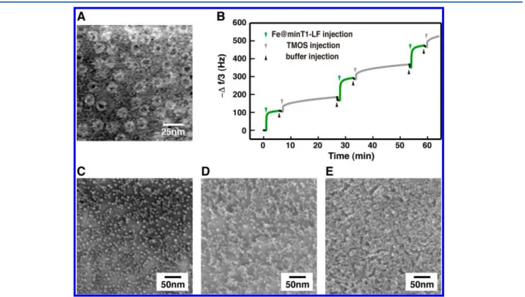
Figure 2. Fabrication of multilayers of BND by BioLBL. (A) TEM image of aurothioglucose-stained Fe@minT1-LF. MinT1-LF shells were unstained (in white). (B) Time-dependent changes in resonance frequency ( f) during QCM analysis. The values on the longitudinal axis represent the negative ofΔf. Changes associated with adsorption of minT1-LF and silicification are shown as green and gray lines, respectively. Green and gray arrows represent the respective time points at which minT1-LF and silicic acid, respectively, were added to the measurement chamber. The black arrows indicate the time points at which the QCM measurement cell was washed with buffer solution. SEM images of samples after fabrication of the (C)first, (D) second, and (E) third Fe@minT1-LF layer.
nodes by BioLBL offers advantages compared to conventional chemical vapor deposition (CVD)21,22 and ion implantation methods,23in which control of the size, shape, position, and density of nanoparticles is difficult to achieve. Use of a size-restricted protein template allows control of nanoparticle size, and specific chemical and biological modification of the substrate surface and protein outer surface enables controlled placement in a desired area on the nanometer scale.24−26 Furthermore, BioLBL enables the 3D integration of a charge storage node layer in the Z-direction,13which is quite difficult using conventional fabrication methods but can be achieved by simple chemical reaction in solution using a BioLBL approach. We fabricate a MOS memory device with a 3D-integrated memory node and confirm that the 3D node can be used as a charge storage node offlash memory.
■
RESULTS AND DISCUSSIONSNatural biomolecules usually need a high concentration of alkaline metal ions such as sodium and potassium present to allow mineralization in solution; TBP-1 and minT1-LF are no exception.13,16 However, contamination with alkaline metal ions degrades a performance of the resulting LSI devices because of the current leakage caused by persisting metal ions. Therefore, we need to decrease ion concentration and optimize solution conditions of the BioLBL process so that they are compatible with LSI. We first searched for an appropriate solution composition that allows minT1-LF to form minerals from prehydrolized tetramethoxysilane (TMOS) without alkaline metal ions. We found that including 50−100 mM of Tris-phosphate buffer enabled silica to mineralize without alkaline metal ions. Although minT1-LF showed inferior binding and mineralization activity under these conditions compared with those of conventional mineralization involving a millimolar concentration of alkaline ions in solution, sufficient binding of minT1-LF to the substrate and subsequent silicafilm formation were confirmed. This indicates that use of 50−100 mM Tris-phosphate buffer is suitable for fabrication of memory nodes for LSI devices. We confirmed that BioLBL can also be performed using minT1-LF containing Fe-BNDs, Fe@minT1-LF (Figure 2A). Formation of multilayered nanostructures during the BioLBL process was confirmed by monitoring the frequency changes of a quartz crystal microbalance (QCM). A profile of resonance frequency changes of the QCM (Figure 2B) was similar to that observed previously.16Initial injection of Fe@minT1-LF solution into the QCM measurement cell caused the resonance frequency to decrease by approximately 100 Hz; this reduction in resonance frequency corresponds to binding of Fe@minT1-LF molecules at 1.7μg/cm2, equivalent
to monolayer deposition.16To confirm this, we also observed surfaces of thefirst Fe@minT1-LF layer by SEM (Figure 2C). After thefirst Fe@minT1-LF monolayer formed, we injected a
layer. Subsequent cycles of injection of TMOS and Fe@minT1-LF solutions caused the changes in resonance frequency, indicating the successful stepwise deposition of alternate layers of Fe@minT1-LF and silica. The frequency change caused by the binding of Fe@minT1-LF is negligible for each layer formation, and therefore, the amount of Fe@minT1-LF adsorbed on each layer is considered to be almost the same. The reproducibility of this BioLBL process was excellent. Those facts suggest that we can produce 3D nanoparticle arrays with consistent node density for use as memory devices.
A commercially available p-Si (100) substrate (∼10 Ω cm) with a 3-nm-thick thermally oxidized tunneling SiO2layer was used to fabricate MOS memory. The SiO2surface was cleaned
with piranha solution and UV/ozone treatment before the BioLBL process. The cleaned silicon substrate was incubated in Fe@minT1-LF solution (0.2 mg/mL) in 100 mM Tris-phosphate buffer at pH 8.0 for 10 min at room temperature and then washed with the same buffer solution. The substrate was then incubated in silicification solution containing 100 mM TMOS, which was prehydrolyzed with 1 mM inorganic phosphate, and 100 mM Tris-phosphate buffer for 20 min at room temperature. After terminating the silicification reaction, the substrate was thoroughly washed with buffer solution to remove residual chemicals. The BioLBL procedure was repeated until the desired number of Fe@minT1-LF layers was formed. Figure 2C−E shows scanning electron microscopy (SEM) images of deposited Fe-BNDs immobilized on the substrate during the BioLBL process. Small particles observed in SEM images correspond to Fe-BNDs of Fe@minT1-LF. An array of multilayered Fe-BNDs was successfully fabricated an increasing density of particles with each layer number increase. Analysis of the SEM images revealed that the aerial density of Fe-BNDs in a single layer is ∼6.7 × 1011 cm−2, which is comparable to the adsorption density of BNDs for MOS memory devices that showed large charge storage capacity reported previously.27,28 Arial density is an important issue to observe for memory operation on floating nanodot gate-type memory. If the dot number is too small, we cannot observe memory operation even though BNDs can store the charge. The fabricated BioLBL memory contains a sufficiently large number of BNDs in each layer, so we can expect to observe charge storage behavior in the BioLBL memory. Following the BioLBL process, outer protein shells were removed by UV oxidation under ozone. Even though the Fe-BNDs are covered with a thin film of mineralized silica, X-ray photoemission spectra (XPS) of carbon and nitrogen suggest that organic residues are removed by chemical decomposition upon UV irradiation (Figure S2, SI). Because the protein shell can be removed by oxidation, the mineralized silica layer is considered porous compared with thermally oxidized SiO2. Fabricated layers of Fe-BNDs were embedded in a SiO2control gate layer
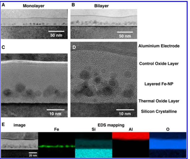
with a thickness of 20 nm, and aluminum electrodes were deposited on both sides of the substrate to make a MOS capacitor device. After deposition of electrodes, devices were annealed at 450°C under reductive gas atmosphere (H2:N2=
10%:90%) for 1 h to improve electrode contact and convert Fe-BNDs to Fe metal.29The fabricated MOS capacitor structure was evaluated by transmission electron microscope (TEM) observation of ultrathin cross sections of the prepared MOS capacitors prepared by ion-milling. TEM images of a monolayer of Fe-BNDs in the MOS stacked structure depicted in Figure 3A,C clearly show that the embedded Fe-BNDs were almost the same shape and size as prepared ones. The BNDs formed a monolayer in the gate SiO2 without merging after device fabrication. Cross-sectional TEM images of a bilayer MOS capacitor structure show that a multilayered architecture of Fe-BNDs can be fabricated easily using BioLBL (Figure 3B,D). Structural analysis of the MOS capacitor by high-resolution scanning TEM (STEM) analysis coupled with energy-dispersive X-ray spectroscopy (EDS) elemental mapping (Figure 3E) clearly illustrates that embedded BNDs did not diffuse into the gate oxide; thus, a layered nanoparticle structure may not be fabricated by both the conventional layer-by-layer technique and conventional LSI process. TEM analysis also indicated that the nanostructure fabricated by BioLBL was robust through the device integration process. These results confirm that multilayered charge storage node arrays for MOS
memory devices can be fabricated by a simple, wet process BioLBL.
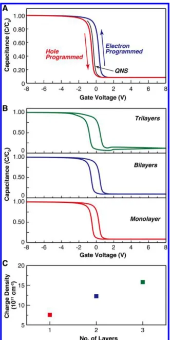
The charge storage characteristics of the fabricated single-layer BioLBL memory were evaluated by high-frequency capacitance−voltage (C−V) measurements (Figure 4A). A C−V curve obtained under a gate voltage (VG) sweep between
−1 and +1 V, a voltage range in which no charge storage can be achieved, shows a sharp transition from accumulation to inversion without hysteresis and corresponds well with the C− V plot of a control sample without Fe-BNDs. Namely, the observed curve corresponds to the quasineutral state (QNS) of embedded BND memory nodes. In contrast, when positive (+10 V, 10 s) or negative (−10 V, 10 s) pulsed VGis applied
before a VGsweep, the C−V curve shifted toward the positive
(blue line in Figure 4A) or negative (red line in Figure 4A) direction, respectively, versus the QNS. A C−V curve shift, i.e., a flat-band voltage (VFB) shift, is typically observed when an
electron and/or hole is injected to thefloating gate. Therefore, the observed VFB shifts clearly indicate that VG
polarity-dependent electron and hole confinement occurs in the embedded BNDs, as we previously observed for BND-embedded MOS memory.27 We should note that MOS memory without Fe-BNDs did not exhibit any VFBshift caused by charge storage in the BNDs. Negligible change in memory window size upon ac frequency variation from 1 kHz to 1 MHz during C−V measurement also suggests that the observed VFB
shift can be attributed to charge confinement in the embedded
Figure 3.Cross-sectional TEM images of BND structures fabricated by BioLBL. TEM image of (A) monolayer and (B) bilayer BND structures for use inflash memory devices. High-resolution TEM images of (C) monolayer and (D) bilayer BND structures, respectively. (E) EDS mapping of a cross-section of the bilayer BND structure in aflash memory device.
BNDs rather than surface charge trapping. Thus, the observed charge confinement-induced VFBshift clearly indicates that the
memory node array fabricated by BioLBL does work as a memory node. We also found that a plasma CVD process and postmetal annealing (PMA) could improve the quality of the porous silica layer formed by silicification, which is generally considered a poor gate oxide. The C−V characteristics of this MOS device showed a low interface density of 1.0× 1011cm−2 eV−1, no frequency dispersion of capacitance density, and no hysteresis in the wide frequency range from 1 kHz to 1 MHz. Therefore, the quality of the control gate is high enough for memory applications, which is probably caused by the conformal deposition of control gate oxide by plasma CVD. SiO2deposited by plasma CVD canfill the pores in the silicified
and holes was monitored by change in capacitance and converted to VFB change.25 Electron and hole programming was performed at +10 and−10 V, respectively, with 3 s pulsed bias. Time-dependent change in capacitance was monitored at +1.0 and −0.4 V for electrons and holes, respectively. After electron programming, VFB gradually decreased for the first
5000 s and then decreased rapidly after 5000 s. The difference between the VFBof the electron-programmed device (+1.4 V) and VFBof the QNS (−0.1 V) at 104s, i.e., the memory window
size (ΔVFB), was still 1.4 V. From the aerial density of the
embedded Fe-BNDs (∼6.7 × 1011 cm−2), the stored charge density can be calculated as 1.8× 1012cm−2. In contrast, VFBof
the hole-programmed device rapidly shifted to the positive voltage side and showed a small ΔVFB of 0.23 V at 104 s.
Although hole retention time was less than that of electrons, both charges can be retained for more than 107 s from
extrapolation of the VFBshift (inset in Figure S3, SI).
To determine the effect of the 3D-integrated multilayered array structure on device properties, BND memories with different numbers of layers, mono-, bi-, and trilayer, were fabricated and their CV characteristics measured, as shown in Figure 4C. One VGsweep between−8 and +8 V starting from
negative voltage was applied. The VG-sweep-induced VFB shift
depends on the polarity of the applied voltage, as observed in Figure 4A, with anticlockwise hysteresis found for all devices. These results indicate that effective charge injection to the BNDs in the upper layers, namely, the second and third layers, can occur, so the BNDs effectively work as charge storage nodes, even though they are further away from the Si substrate surface than thefirst layer. As seen in Figure 4B, the curves of the fabricated multilayered memory devices showed a monotonic increase of ΔVFB depending on the number of
layers. Figure 4C depicts the change in charge density for devices with different layer number. The charge density for each device was calculated from the aerial density of embedded Fe-BNDs. Stored charge densities for single-, double-, and triple-layer memory devices was calculated to be 7.6 × 10¹¹, 12.3× 10¹¹, and 15.8× 1011cm−2. SEM observation and QCM results indicate that the number density of Fe-BNDs in the fabricated memory increases linearly with layer number. Therefore, the observed linear increase of stored charge density, i.e., memory window size, is interrupted by the increase in the number of embedded BNDs in the charge storage node. This result clearly indicates that multilayered memory node arrays fabricated by the BioLBL method can be used as integrated memory nodes. We also made multilayered BND-embedded memory with a field effect transistor, which has been reported elsewhere.31This study demonstrates that nanofabrication processes using a biological function can be adapted for LSI devices. Device properties can be improved
Figure 4.(A) Capacitance−voltage characteristics of single-layer Fe-BND-embedded BioLBL memory. Black, blue, and red lines depict QNS C−V without charge injection and C−V after charge injection with +10 V and−10 V gate pulses for 10 s, respectively. (B) C−V curves of BioLBL memory with different layer numbers. VGwas swept
from−8 V to +8 V and then returned to −8 V. (C) Stored charge density for BioLBL memories with different layer numbers depicted in part B.
using our BioLBL method because of the vertical buildup of charge storage elements.
■
CONCLUSIONA novel process to fabricate hierarchical nanoarchitectures of multilayered nanodots is demonstrated, and the nanoarchitec-tures are applied in memory devices. Memory nodes made up of biochemically synthesized BNDs in protein cavities were fabricated by BIoLBL using the specific binding and mineralization function of peptide aptamer minTBP-1 attached to the exterior of recombinant minT1-LF. MinT1-LF successfully aligned to form separate layers using the wet chemical process of BioLBL. The fabricated Fe-BND array was embedded into a stacked MOS device structure as a charge storage node. The MOS capacitor showed memory operation, and an increase of BND layer number increased the charge storage ability of the memory device. In this study, we only examined Fe@minT1-LF in MOS capacitors; however, ferritin can incorporate various kinds of nanoparticles in its cavity, not only by biomineralization but also by nanoparticle-directed assembly. By using different nanoparticles encapsulated in minT1-LF, we can fabricate heterogeneous layers of different nanoparticles with divergent electronic properties such as band gap.16This approach can be used to develop novel types of multilayered memory devices. Moreover, applications of heterogeneous nanoparticle multilayers made by the BioLBL method are not restricted to memory devices but can be applied to optoelectronics, battery cells, and so on.32−34
■
METHODSPreparation of minT1-LF. Construction, expression, and purification of minT1-LF have been described previously.14 Purified apo-minT1-LF molecules werefilled with ferrihydrite nanoparticles as described to obtain [email protected] remove alkaline metal ions, we carried out extensive dialysis against 100 mM Tris-phosphate buffer at pH 8.0. The concentration of Fe@minT1-LF was determined using the Bradford method using apo-minT1-LF as a calibration standard.
BioLBL without Alkaline Metal Ions. Silicification activities of apo-minT1-LF were monitored as described previously,14 and we found buffer conditions for silicification that were alkaline metal ion free. We then monitored the BioLBL process using new solution conditions on the quartz sensor of a QCM-D300 (Q-sense AB, Göteborg). The temperature of the chamber was kept at 25.00 ± 0.05 °C, and QCM data were collected at 14.8 MHz. We used a titanium-coated sensor, which was purchased from Q-sense AB. Experimental conditions in Figure 2B were as follows. Wefirst applied the Ti-coated sensor after filling the measurement cell with 0.2 mg/mL of Fe@ minT1-LF in 100 mM Tris-phosphate buffer at pH 8.0 and incubation for about 5 min. The measurement cell was washed with same buffer solution, and then we introduced a silicification solution composed of 0.1 M TMOS, which was prehydrolyzed with 1 mM inorganic phosphate and 100 mM Tris-phosphate buffer. After about 20 min incubation, we washed the measurement cell with buffer solution. We repeated these steps of Fe@minT1-LF binding and silicification three times.
Preparation and Evaluation of MOS Capacitor with Floating Nanodot Gate. Commercially available p-Si (100) substrate (∼10 Ω cm) with a 3-nm-thick thermally oxidized tunneling SiO2 layer was
used as the substrate for MOS capacitor fabrication. The SiO2surface
of the substrate was made hydrophilic by UV irradiation under ozone prior to BioLBL. Layered memory nodes were fabricated by sequential binding and silicification steps following the BioLBL process described above. The protein component of Fe@minT1-LF, which is an impurity that could affect device operation, was removed by UV irradiation under ozone at 115°C for 60 min. Each fabricated Fe-BND array was buried in a 17-nm-thick control gate oxide by plasma CVD
using a tetraethoxysilane as a source gas. Aluminum metal was used as the metal gate electrode of the MOS capacitors. PMA was performed in a reductive gas atmosphere (10% H2in 90% N2) at 450°C for 1h. It
should be noted that the partial reduction of Fe-BNDs occurred during PMA under the reductive atmosphere. Electrical character-ization of the fabricated Fe-BND-embedded BioLBL memory arrays was performed by capacitance−voltage (C−V) measurements with an HP 4284A LCR meter for MOS capacitors. All measurements were performed at room temperature.
Electron Microscope Observation. We conducted high-resolution SEM (SEM7400F, JEOL) measurements to observe nanoparticle deposition by BioLBL. The SEM was operated at a low acceleration voltage of 5 kV to observe the spatial distribution of Fe-BNDs in the mineralized silica layer. Samples for cross-sectional samples for TEM and STEM observations were prepared as described previously (outsourced to TOPCON, Tokyo, Japan).16
■
ASSOCIATED CONTENT*
S Supporting InformationMore extensive characterization of multilayered devices, the elemental analysis, and the charge retention properties. This material is available free of charge via the Internet at http:// pubs.acs.org.
■
AUTHOR INFORMATIONCorresponding Authors
* K.-I.S. e-mail: [email protected]. *A.M. e-mail: [email protected].
Present Addresses
⊥Faculty of Innovative Systems Engineering, Nippon Institute
of Technology, Miyashiro-machi, Saitama 345-8501, Japan.
#H. H. Wills Physics Laboratory, School of Physics, University
of Bristol, Tyndall Avenue, Bristol BS8 1TL, United Kingdom.
Author Contributions
∇These authors contributed equally.
Notes
The authors declare no competingfinancial interest.
■
ACKNOWLEDGMENTSThis work was partially supported by a Grant-in-aid for Scientific Research from the Ministry of Education, Science, Sports and Culture, Japan to K.S., and a Grant-in-Aid for Young Scientists (A) from the Japan Society for Promotion of Science to K.-I. S. (20681013), a Grant-in-Aid for Young Scientists (B) from the Japan Society for Promotion of Science to A.M. (19750162), and a Leading Project of the Ministry of Education, Culture, Sports, Science and Technology, Japan to I.Y.
■
REFERENCES(1) Sarikaya, M.; Tamerler, C.; Schwartz, D. T.; Baneyx, F. Materials Assembly and Formation using Engineered Polypeptides. Annu. Rev. Mater. Res. 2004, 34, 373−408.
(2) Dickerson, M. B.; Sandhage, K. H.; Naik, R. R. The Protein and Peptide-Directed Syntheses of Inorganic Materials. Chem. Rev. 2008, 108, 4935−4978.
(3) Yamashita, I. Fabrication of a Two-Dimensional Array of Nano-Particles using Ferritin Molecule. Thin Solid Film 2001, 393, 12−18.
(4) Sarikaya, M.; Tamerler, C.; Jen, A. K.-Y.; Schulten, K.; Baneyx, F. Molecular Biomimetics: Nanotechnology through Biology. Nat. Mater. 2003, 2, 577−585.
(5) Tang, S.; Mao, C.; Liu, Y.; Kelly, D. Q.; Banerjee, S. K. Nanocrystal Flash Memory Fabricated with Protein-Mediated Assembly. Tech. Dig. - Int. Electron Devices Meet. 2005, 174−177.
Directed Nanocrystal Assembly. Nature 2000, 405, 665−668. (11) Sano, K.; Shiba, K. A Hexapeptide Motif that Electrostatically Binds to the Surface of Titanium. J. Am. Chem. Soc. 2003, 125, 14234− 14235.
(12) Sano, K.; Sasaki, H.; Shiba, K. Specificity and Biomineralization Activities of Ti-Binding Peptide-1 (TBP-1). Langmuir 2005, 21, 3090−3095.
(13) Sano, K.; Yoshii, S.; Yamashita, I.; Shiba, K. In Aqua Structuralization of a Three-Dimensional Configuration using Biomolecules. Nano Lett. 2007, 7, 3200−3202.
(14) Sano, K.; Ajima, K.; Iwahori, K.; Yudasaka, M.; Iijima, S.; Yamashita, I.; Shiba, K. Endowing a Ferritin-like Cage Protein with High Affinity and Selectivity for Certain Inorganic Materials. Small 2005, 1, 826−832.
(15) Sano, K.; Shiba, K. Stepwise Accumulation of Layers of Aptamer-Ornamed Ferritins using Biomimetic Layer-By-Layer. J. Mater. Res. 2008, 23, 3236−3240.
(16) Sano, K.; Sasaki, H.; Shiba, K. Utilization of the Pleiotropy of a Peptidic Aptamer To Fabricate Heterogeneous Nano-Dot-Containing Multilayer Nanostructures. J. Am. Chem. Soc. 2006, 128, 1717−1722. (17) Banyard, S. H.; Stammers, D. K.; Harrison, P. M. Electron Density Map of Apoferritin at 2.8-A Resolution. Nature 1978, 271, 282−284.
(18) Iwahori, K.; Yoshizawa, K.; Muraoka, M.; Yamashita, I. Fabrication of ZnSe Nanoparticles in the Apoferritin Cavity by Designing a Slow Chemical Reaction System. Inorg. Chem. 2005, 44, 6393−6400.
(19) Okuda, M.; Iwahori, K.; Yamashita, I.; Yoshimura, H. Fabrication of Nickel and Chromium Nanoparticles using the Protein Cage of Apoferritin. Biotechnol. Bioeng. 2003, 84, 187−194.
(20) Tsukamoto, R.; Iwahori, K.; Muraoka, M.; Yamashita, I. Synthesis of Co3O4 Nanoparticles Using the Cage-Shaped Protein,
Apoferritin. Bull. Chem. Soc. Jpn. 2005, 78, 2075−2081.
(21) Tiwari, S.; Rana, F.; Chan, K.; Shi, K.; Hanafi, H. Single Charge and Confinement Effects in Nano-Crystal Memories. Appl. Phys. Lett. 1996, 69, 1232−1234.
(22) Tiwari, S.; Rana, F.; Hanafi, H.; Hartstein, A.; Crabbe, E. F.; Chan, K. A Silicon Nanocrystals Based Memory. Appl. Phys. Lett. 1996, 68, 1377−1379.
(23) Kapetanakis, E.; Normand, P.; Tsoukalas, D.; Beltsios, K. Room-Temperature Single-Electron Charging Phenomena in Large-Area Nanocrystal Memory Obtained by Low-Energy Ion Beam Synthesis. Appl. Phys. Lett. 2002, 80, 2794−2796.
(24) Kumagai, S.; Yoshii, S.; Yamada, K.; Matsukawa, N.; Fujiwara, I.; Iwahori, K.; Yamashita, I. Electrostatic Placement of Single Ferritin Molecules. Appl. Phys. Lett. 2002, 88, 153103.
(25) Miura, A.; Uraoka, Y.; Fuyuki, T.; Yoshii, S.; Yamashita, I. Floating Nanodot Gate Memory Fabrication with Biomineralized Nanodot as Charge Storage Node. J. Appl. Phys. 2008, 103, 074503.
(26) Yamada, K.; Yoshii, S.; Kumagai, S.; Miura, A.; Uraoka, Y.; Fuyuki, T.; Yamashita, I. Effects of Dot Density and Dot Size on Charge Injection Characteristics in Nanodot Array Produced by Protein Supramolecules. Jpn. J. Appl. Phys. 2007, 46, 7549−7553.
(27) Miura, A.; Hikono, T.; Matsumura, T.; Yano, H.; Hatayama, T.; Uraoka, Y.; Fuyuki, T.; Yoshii, S.; Yamashita, I. Floating Nanodot Gate
Protein Supramolecule. Jpn. J. Appl. Phys. 2006, 45, 8946−8951. (31) Ohara, K.; Zheng, B.; Uenuma, M.; Ishiwaka, Y.; Shiba, K.; Yamashita, I.; Uraoka, Y. Three-Dimensional Nanodot-Type Floating Gate Memory Fabricated by Bio-Layer-by-Layer Method. Appl. Phys. Exp. 2011, 4, 085004.
(32) Liang, R.; Xu, S.; Yan, D.; Shi, W.; Tian, R.; Yan, H.; Wei, M.; Evans, D. G.; Duana, X. CdTe Quantum Dots/Layered Double Hydroxide Ultrathin Films with Multicolor Light Emission via Layer-by-Layer Assembly. Adv. Funct. Mater. 2012, 22, 4940−4948.
(33) Liang, R.; Tuan, R.; Shi, E.; liu, Z.; Yan, D.; Wei, M.; Evans, D. G.; Duana, X. A Temperature Sensor Based on CdTe Quantum Dots-Layered Double Hydroxide Ultrathin Films via Layer-by-Layer Assembly. Chem. Commun. 2013, 49, 969−971.
(34) Nam, K. T.; Kim, D.-W.; Yoo, P. J.; Chiang, C.-Y.; Meethong, N.; Hammond, P. T.; Chiang, Y.-M.; Belcher, A. M. Virus-Enabled Synthesis and Assembly of Nanowires for Lithium Ion Battery Electrodes. Science 2006, 312, 885−888.