Photoluminescence and photoluminescence excitation studies of as-grown and
P-implanted GaN: On the nature of yellow luminescence
H. Y. Huang, C. H. Chuang, C. K. Shu, Y. C. Pan, W. H. Lee, W. K. Chen, W. H. Chen, and M. C. Lee
Citation: Applied Physics Letters 80, 3349 (2002); doi: 10.1063/1.1476400 View online: http://dx.doi.org/10.1063/1.1476400
View Table of Contents: http://scitation.aip.org/content/aip/journal/apl/80/18?ver=pdfcov
Published by the AIP Publishing
Articles you may be interested in
Properties of the main Mg-related acceptors in GaN from optical and structural studies
J. Appl. Phys. 115, 053507 (2014); 10.1063/1.4862928
Nature of the AX center participating persistent photoconductivity effect in As-doped p-ZnO
J. Appl. Phys. 114, 053504 (2013); 10.1063/1.4817246
Critical Mg doping on the blue-light emission in p -type GaN thin films grown by metal–organic chemical-vapor deposition
J. Vac. Sci. Technol. A 21, 134 (2003); 10.1116/1.1524148
Electrical isolation of GaN by ion implantation damage: Experiment and model
Appl. Phys. Lett. 74, 2441 (1999); 10.1063/1.123874
Structural defects and microstrain in GaN induced by Mg ion implantation
J. Appl. Phys. 83, 5992 (1998); 10.1063/1.367465
This article is copyrighted as indicated in the article. Reuse of AIP content is subject to the terms at: http://scitation.aip.org/termsconditions. Downloaded to IP: 140.113.38.11 On: Thu, 01 May 2014 06:19:58
Photoluminescence and photoluminescence excitation studies of as-grown
and P-implanted GaN: On the nature of yellow luminescence
H. Y. Huang,a) C. H. Chuang, C. K. Shu, Y. C. Pan, W. H. Lee, W. K. Chen, W. H. Chen, and M. C. Lee
Department of Electrophysics, National Chiao Tung University, Hsinchu, 300, Taiwan, R. O. C.
共Received 27 December 2001; accepted for publication 6 March 2002兲
We have studied optical and electronic properties of isoelectronic P-implanted GaN films grown by metalorganic chemical vapor phase epitaxy. After rapid thermal annealing, a strong emission band around 430 nm was observed, which is attributed to the recombination of exciton bound to isoelectronic P-hole traps. From the Arrhenius plot, the hole binding energy of⬃180 meV and the exciton localization energy of 28 meV were obtained. According to first-principle total-energy calculations, the implantation process likely introduced NI and P-related defects. By using
photoluminescence excitation technique, we found that the P-implantation-induced localized states not only increase the yellow luminescence but also suppress the transitions from the free carriers to deep levels. © 2002 American Institute of Physics. 关DOI: 10.1063/1.1476400兴
Although the group-III nitride materials have been fab-ricated for ultraviolet-to-green light-emitting diodes, laser di-odes, vertical cavity surface emitting lasers and heterojunc-tion bipolar transistors,1–3they are still having a high defect density problem due to large lattice mismatch. Isoelectronic doping has demonstrated improved crystalline quality as well as the electrical and optical properties in typical III–V and II–VI semiconductors, for instance, N-doped GaP 共Ref. 4兲 and In-doped GaAs.5,6 Previously, we studied the isoelec-tronic In-doped GaN grown by metalorganic chemical vapor phase epitaxy, and found that the small mount of In atom incorporation indeed brought improvements on the optical, electronic, and crystal qualities.7–9In this work, we extended to the group-V elements using the isoelectronic P implanta-tion into GaN and investigated its effects on optical and elec-trical properties.
The undoped GaN films were grown on the共0001兲 sap-phire substrate at 1050 °C by MOVPE. The P-implanted GaN 共GaN:P兲 films were prepared with different doses be-tween 1014 and 1016 cm⫺2. The samples were later treated with rapid thermal annealing共RTA兲 at a temperature 1100 °C for different durations 共10, 20, and 30 s兲 under flowing N2
gas using proximity cap method to recover implantation damages. For the photoluminescence共PL兲 measurements, we utilized a He–Cd laser 共Kimmon IK 5552R-F兲 operating at 325 nm for above-band-gap excitation, and a 0.5 m mono-chromator and a photomultiplier tube 共Hamamatsu R-955兲 for detection. The samples were held in a closed-cycle refrig-erator共APD Cryogenics HC-2兲 for temperature varying mea-surements between 18 and 300 K. For photoluminescence excitation共PLE兲 measurements, we used a 150 W Xenon arc lamp combined with a scanning monochromator 共PTI 101兲 as an excitation light source. The luminescence signals were detected by the same PL system. The PLE spectra were all corrected by the Xe light source response.
Despite of impressive progresses made in the GaN-based devices, there are numbers of defects in this wide band gap
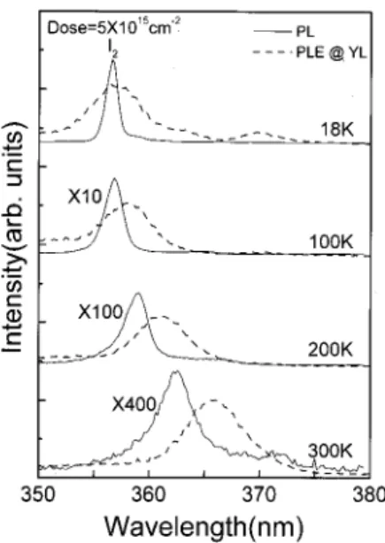
material remained to be studied.10–12Some of them are re-sponsible for forming deep levels that give rise to the noto-rious ‘‘yellow luminescence’’ 共YL兲 共Fig. 1兲. In addition to the YL intensified in increasing temperatures, the prominent
I2 line at 357 nm 共donor bound exciton, D0X兲 is the only
dominant peak at low temperature. This reveals that not only that the bound exciton is ionized but deep levels are also activated significantly at a high temperature. Researchers of-ten infer the film quality by the inof-tensity ratio of YL to I2.
Conventionally, there are two major models interpreting the YL transition. One proposed by Glaser argued that the YL is from the deep double-donor to shallow 共effective-mass兲 acceptor transition.13 The other one proposed by Ogino and Aoki,14 and also by Hofmann et al.,15 attributed the YL to the radiative recombination between shallow-donor to deep localized acceptor levels. According to Jenkins
et al.16 the neutral antisite, NGa, is such a deep-hole trap.
a兲Electronic mail: [email protected] FIG. 1. The temperature dependent PL of as-grown GaN and PLE spectramonitored at YL.
APPLIED PHYSICS LETTERS VOLUME 80, NUMBER 18 6 MAY 2002
3349
0003-6951/2002/80(18)/3349/3/$19.00 © 2002 American Institute of Physics
This article is copyrighted as indicated in the article. Reuse of AIP content is subject to the terms at: http://scitation.aip.org/termsconditions. Downloaded to IP: 140.113.38.11 On: Thu, 01 May 2014 06:19:58
Mattila et al. argued that since a strong electron–phonon in-teraction is associated with the large atomic displacement of
NGa, it is likely to be a favor candidate for the YL. 17
Our measured Raman A1 共LO兲 mode showed significant
broad-ening, the electron–phonon coupling might also involved in the wide YL transition.
To investigate the transition channels for the YL, we have probed its peak signals at 550 nm with the PLE spec-troscopy and observed a clear absorption step about the band gap energy 共see the broken line in Fig. 1兲. Since this step overlaps with the I2 line, it shows the broadness of
absorp-tion edge contributing to the YL intensity. As the temperature is raised above 100 K, some levels slightly lower than that for the I2 line may also help the YL transition. It is
reason-able to infer that nearly all of the native shallow-donor levels are occupied at low temperature so that transitions to them from the valence band are effectively prohibited. At higher temperatures, a significant fraction of the donors is ionized to allow increased photoexcitation to these levels. Therefore, the PLE studies of as-grown GaN have revealed the connec-tion between the native shallow donors and the YL.
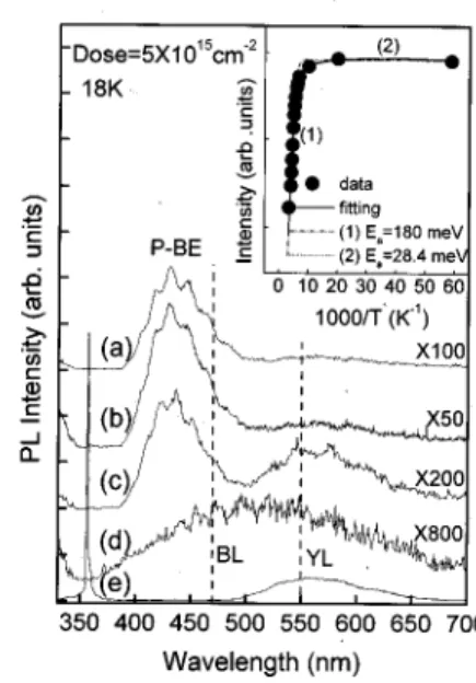
We next address whether the YL profile is affected by ion implantation. We found that the Raman E2mode has an insignificant shift but broadens only slightly so that the crys-talline structure of GaN:P should remain essentially un-changed. However, drastic changes in the PL spectra were observed in Fig. 2. First, the prominent I2 line is quenched.
Second, a new broad band appears around 467 nm共2.65 eV兲. This blue luminescence共BL兲 becomes dominant at the high-est dose along with the residual YL. Thus, it is obvious that the implantation process produced extra deep levels that are responsible for the BL. According to two first-principle total energy calculations the nitrogen interstitial defect, NI, is a
single deep acceptor at approximately 1 eV above the va-lence band maximum.18,19Ab initio calculations showed that
the native nitrogen vacancy defect, VN, is a shallow donor in
high concentration. We tend to ascribe the BL to the radiative
recombination between VN and NI 共and/or other P-related
defect levels兲 caused by P-implantation 共refer to the sche-matic diagram in the inset of Fig. 2兲.
As far as the PLE spectra probed at the YL for GaN:P are concerned, we have detected a rather intense and also broad peak next to the I2 line, instead of the step profile
observed in the as-grown GaN共see the dashed curves in Fig. 2兲. Obviously, the P implantation also generated additional localized states just below the native shallow-donor level that can greatly enhance the YL through below band gap absorption. It is noticed that these localized states have un-even distribution toward the low energy side with the in-creasing dose, reflecting implantation-induced defect levels are deeper than that of the shallow donor. Besides, they ap-pear to be more efficient than the shallow donors in relaxing excess carriers in the conduction band to quench the I2line.
Pankove et al. used different ions for implantation into GaN and also observed such an enhancement effect in YL.20 Gue´naud et al. studied Fe-implanted GaN and suggested that band-to-band absorption can contribute to both the I2and YL
emissions while bound exciton absorption preferentially en-hance the YL than the I2.21 Our PLE results for GaN:P
seemed to agree with these views and therefore, allowed us to attribute these localized states to the disorder induced by the implantation process. They would not be discoverd if the PLE technique had not been utilized.
Since the defect levels associated with the YL are unde-sirable, they need to be reduced as much as possible. The RTA is a commonly employed as a remedy to improve sample quality. After the RTA treatment at 1100 °C for 10, 20, and 30 s for different dosages, we measured the PLE profile again. The results become more symmetric without peak position shift as if the levels on the low energy side are renormalized. However, this profile is still broader than the
I2line and peaked at⬃2 nm toward the red side independent
of annealing duration. Only by varying the sample tempera-ture, the PLE peak is found to shift with respect to the I2line
of as-grown GaN 共see Fig. 3兲. Obviously, a new impurity
FIG. 2. The 18 K PL spectra of GaN:P under different P-implantation doses.
共a兲 1016cm⫺2, 共b兲 5⫻1015cm⫺2, 共c兲 1015cm⫺2, 共d兲 5⫻1014cm⫺2, 共e兲
1014cm⫺2, and共f兲 unimplanted. The dashed curves show the room tempera-ture PLE spectra.
FIG. 3. The temperature dependent PLE spectra of P-implanted (5
⫻1015cm⫺2) GaN after 30 s RTA compared with the I
2line of as-grown
GaN.
3350 Appl. Phys. Lett., Vol. 80, No. 18, 6 May 2002 Huanget al.
This article is copyrighted as indicated in the article. Reuse of AIP content is subject to the terms at: http://scitation.aip.org/termsconditions. Downloaded to IP: 140.113.38.11 On: Thu, 01 May 2014 06:19:58
band 共from localized states兲 near the shallow-donor level must have formed in GaN:P that provides a more efficient relaxation channel for the YL than the usual band-to-band transitions in as-grown sample.
Dramatic changes in the low temperature PL spectra were also observed after annealing. As shown in Fig. 4, the
I2 line is still absent, but a large blue-violet共BV兲 emission band having a width more than 60 nm appears at 430 nm 共2.88 eV兲. This BV band is likely to be the shifted BL band of the unannealed GaN:P. One report had attributed it to the recombination of excitons bound to isoelectronic-P trap 共P-BE兲 at the N site (PN). Because the electronegativity of P
共2.19兲 is smaller than that of N 共3.04兲 (⬃28%),22 the
isoelectronic-P potential becomes more attractive to a hole. Besides, the large lattice distortion due to larger P-atomic size induces hole-like traps and forms holes. These traps can capture free electrons creating bound excitons or interact with electrons at donor site to make D-to-P trap transitions. By increasing the annealing duration, the intensity ratio of P-BE to YL also increases while the P-BE line width de-creases. Thus, the PNsubstitution is increased that apparently
suppresses the relaxation transition from the shallow donor to the deep levels. Because of the microcavity effect, quite a few oscillations on top of this new emission band are also observed.23 They reveal that the annealing process not only recovers NI defects formed by P implantation but also makes
better surface perfection and interface flatness.
By drawing the temperature dependent intensity of P-BE in an Arrhenius plot共see the inset of Fig. 4兲, we obtained two activation energies: the hole binding energy (Ea1) at the
isoelectronic-P trap and the exciton localization energy (Ea2).24Ea1 is 180共168兲 meV that is much larger than Ea2 of 28 共17兲 meV after 30 共20兲 s of RTA. Because the I2 localization energy共5.3 meV兲25is much smaller than that of P-trap, the excited free excitons tend to be trapped.
There-fore, it is clear that RTA process makes the PN substitution
more consolidated. Additionally, Hall measurements showed that the reduced mobility (⬃2 cm/V s) and increased con-centration (⬃2.9⫻1017 cm⫺3) due to implantation can be recovered共⬃142 cm/V s, ⬃6⫻1016 cm⫺3兲 just after 10 s of RTA. This also supports improved PNsubstitution that
appar-ently suppresses the relaxation transition from the free carri-ers to the deep levels.
In summary, we have examined the P-implanted GaN by using the PL and PLE spectroscopies. The results revealed that the YL is not only associated with deep levels, but also closely related to the implantation-induced defects that showed a localized distribution. The new PL emission peak is attributed to the P-BE that showed two activation energies.
The authors wish to acknowledge support by the Na-tional Science Council of the Republic of China under Con-tract No. NSC89-2112-M009-056 89R197.
1Y.-K. Song, H. Zhou, M. Diagne, A. V. Nurmikko, R. P. Schneider, Jr., C.
P. Kuo, M. R. Krames, R. S. Kern, C. Carter-Coman, and F. A. Kish, Appl. Phys. Lett. 76, 1662共2000兲, and references therein.
2
S. Nakamura, M. Senoh, S. Nagahama, N. Iwasa, T. Yamada, T. Mat-sushita, H. Kiyoku, and Y. Sugimoto, Jpn. J. Appl. Phys., Part 2 35, L74 共1996兲.
3J. M. Redwig, D. A. S. Loeber, N. G. Anderson, M. A. Tischler, and J. S.
Flynn, Appl. Phys. Lett. 69, 1共1996兲.
4
D. G. Thomas, J. J. Hopfield, and C. J. Frosch, Phys. Rev. Lett. 15, 857 共1965兲.
5P. K. Bhattacjharya, S. Dhar, P. Berger, and F. Y. Juang, Appl. Phys. Lett. 49, 470共1986兲.
6
W. Walukiewicz, Appl. Phys. Lett. 54, 2009共1989兲.
7
C. K. Shu, J. Ou, H. C. Lin, W. K. Chen, and M. C. Lee, Appl. Phys. Lett. 73, 641共1998兲.
8C. K. Shu, W. H. Lee, Y. C. Pan, C. C. Chen, H. C. Lin, J. Ou, W. H.
Chen, W. K. Chen, and M. C. Lee, Solid State Commun. 114, 291共2000兲.
9
H. Kumano, K. I. Koshi, S. Tanaka, I. Suemune, X. Q. Shen, P. Riblet, P. Ramvall, and Y. Aoyagi, Appl. Phys. Lett. 75, 2879共1999兲.
10U. Jahn, J. Menniger, O. Brandt, H. Yang, and K. H. Ploog, Proceedings of the 23rd International Conference on the Physics of Semiconductors
共World Scientific, Singapore 1996兲, p. 2857
11
H. J. Queisser, Appl. Phys. 10, 275共1976兲.
12T. Suski, P. Perlin, H. Teisseyre, M. Leszxzynski, I. Grzegory, J. Jun, M.
Bockowski, S. Porowski, and T. D. Moustakas, Appl. Phys. Lett. 67, 2188 共1995兲.
13
E. R. Glaser, T. A. Kennedy, K. Doverspike, L. B. Rowland, D. K. Gaskill, J. A. Freitas, Jr., M. A. Khan, D. T. Olson, J. N. Kuznia, and D. K. Wickenden, Phys. Rev. B 51, 13326共1995兲.
14T. Ogino and M. Aoki, Jpn. J. Appl. Phys., Part 1 19, 2395共1980兲. 15
A. Hofmann, L. Eckey, P. Maxim, J.-Chr. Holst, R. Heitz, D. M. Hofmann, D. Kovalev, G. Steude, D. Volm, B. K. Meyer, T. Detchprohm, H. Amano, and I. Akasaki, Solid-State Electron. 41, 275共1997兲.
16D. W. Jenkins and J. D. Dow, Phys. Rev. B 39, 3317共1989兲.
17T. Mattila, A. P. Seitsonen, and R. M. Nieminen, Phys. Rev. B 54, 1474
共1996兲.
18J. Neugebauer and C. G. Van de Walle, Phys. Rev. B 50, 8067共1994兲. 19P. Boguslawski, E. L. Briggs, and J. Bernholc, Phys. Rev. B 51, 17255
共1995兲.
20J. I. Pankove and J. A. Hutchby, J. Appl. Phys. 47, 5387共1976兲. 21
C. Gue´naud, E. Deleporte, M. Voos, and C. Delalande, MRS J. Nitride Semicond. Res. 2, 10共1997兲.
22W. M. Jadwisienczak and H. J. Lozykowski, Mater. Res. Soc. Symp. Proc. 482, 1033共1998兲.
23
A. Billeb, Appl. Phys. Lett. 70, 2790共1997兲.
24
D. Bimberg and M. Sondergeld, Phys. Rev. B 4, 3451共1971兲.
25K. Pakula, A. Wysmolek, K. P. Korona, J. M. Baranowski, R. Stepniewski,
I. Grzegory, M. Bockowski, J. Jun, S. Krukowski, M. Wroblewski, and S. Porowski, Solid State Commun. 97, 919共1996兲.
FIG. 4. The 18 K PL spectra of P-implanted GaN after RTA.共a兲 30 s, 共b兲 20 s,共c兲 10 s, 共d兲 as-implanted, and 共e兲 as-grown.
3351
Appl. Phys. Lett., Vol. 80, No. 18, 6 May 2002 Huanget al.
This article is copyrighted as indicated in the article. Reuse of AIP content is subject to the terms at: http://scitation.aip.org/termsconditions. Downloaded to IP: 140.113.38.11 On: Thu, 01 May 2014 06:19:58