Vol. 132, No. 5
I n P E P I T A X I A L L A Y E R S 1193 Manuscript s u b m i t t e d April 30, 1984; revised manu-script received Oct. 29, 1984.
AT&T Bell Laboratories assisted in meeting the publica-
tion costs of this article.
R E F E R E N C E S
1. G.H. Olson, C. J. Nuese, and M.
Ettenberg, Appl. Phys.
Let.,
34, 262 (1979).2. W. D. J o h n s t o n , Jr., and K. E. Strege, I E E E 38th Device Research Conference, Abstract Vol. IV B-3, Ithaca, N e w York (1980).
3. G.H. Olson, in " G a I n A s P Alloy S e m i c o n d u c t o r s , " T. P. Pearsall, Editor, Chap. 1, J o h n Wiley and Sons, New York (1982).
4. S. N. G. Chu,
This Journal,
129, 2082 (1982).5. S. N. G. Chu, C. M. Jodlauk, and A. A. Ballman,
ibid.,
129, 352 (1982).6. S. N. G. Chu and T. T. Sheng,
ibid.,
To be published. 7. R. E. Nahory, M. A. Pollack, W. D. Johnston, Jr., andR. L. Barns,
Appl. Phys. Lett.,
33, 659 (1978). 8. C. N. Cochran and L. M. Foster,This Journal,
1{}9, 144(1962).
9. D. Shaw,
J. Phys. Chem. Solids,
36, 111 (1975). 10 C. D. T h u r m o n d ,ibid.,
26, 785 (1965).11. M. G e r s h e n z o n and R. H. Mikulyak,
This Journal,
198, 548 (1961).12. A. K o u k i t u and H. Seki,
J. Cryst. Growth,
49, 325 (1980). 13. R.F. Karlicek, Jr., and A. B. LaRoe, U n p u b l i s h e d work. 14. V. M. Donnelly and R. F. Karlicek,J. Appl. Phys.,
53,6399 (1982).
Resistance Switching Characteristics in Polycrystalline Silicon Film
Resistors
Chih-Yuan Lu*
AT&T Bell Laboratories, Reading, Pennsylvania 19603-0856; Institute of Electronics, National Chiao-Tung University,
Hsin-Chu, Taiwan, 300, China; Department of Electrical and Computer Engineering, North Carolina State University,
Raleigh, North Carolina 27695-7911
Nicky Chau-Chun Lu
IBM T J . Watson Research Center, Yorktown Heights, New York 10598
Chih-Ching Shih
Institute of Electronics, National Chiao-Tung University, Hsin~Chu, Taiwan 300, China
A B S T R A C T
B o t h reversible and irreversible resistance switchings have been investigated in boron- and arsenic-doped L P C V D polycrystalline silicon film resistors. The effects of film thickness and doping concentration on the transition voltage and current h a v e b e e n characterized for different length resistors having film thickness from 0.1 to 1.2 t~m and doping concentration ranging from 5 • 10 TM to 1 • 10 z~ cm -3. U n d e r a large voltage bias, the resistor can be switched to a conduc-
tive " o n " state or to a "short" state having resistance reduction by a factor of 103-106, or it can be b l o w n "open". The tran- sition voltage and current and the resistance after switching depend strongly on film thickness, doping concentration, and applied power. A simple qualitative m o d e l is proposed to explain these resistance switching p h e n o m e n a .
Polycrystalline silicon (polysilicon) films have been widely used as solar cell and integrated-circuit elements, and such applications have stimulated extensive studies of the electrical properties of this material. B o t h revers- ible and irreversible resistance switching p h e n o m e n a have b e e n reported (1-3). The irreversible resistance switching has b e e n extensively applied to integrated- circuit applications, such as a m e m o r y e l e m e n t in fusible- link P R O M ' s (3-5) and a fuse or antifuse in r e d u n d a n c y circuits in high density RAM's (6). However, there are a limited n u m b e r of papers in the literature systematically studying resistance switching properties of polysilicon re- sistors. Greve studied the p r o g r a m m i n g m e c h a n i s m of heavily d o p e d polysilicon resistor fuses and showed that formation of a s e c o n d - b r e a k d o w n state is necessary to blow open the fuses (1). He also studied n~-p-n § polysilicon devices and showed that the dopant migration and the a l u m i n u m penetration in m o l t e n filaments through polysilicon devices are the m e c h a n i s m s for re- sistance switching (7, 8). On the other hand, Mahan re- ported a reversible switching p h e n o m e n o n in u n d o p e d polysilicon resistors having high v a l u e resistance (2).
This work reports n e w e x p e r i m e n t a l results on the ef- fects of film thickness, doping concentration, and device dimensions on resistance switching behavior in poly- silicon resistors. The resistances before and after switch- ing, the switching IrV curves, and the transition voltage
*Electrochemical Society Active Member.
and current beyond which the switching occurs were characterized extensively. Different switching patterns have b e e n clearly identified from this systematic study, and a better physical understanding of the switching be- havior in polysilicon resistors has b e e n obtained from a qualitative model.
Sample Preparation and Measurements
A 0.80 tLm thick oxide was grown at ll00~ on top of N-type (100) silicon wafers with resistivity of 4 - 7 ~l-cm. U n d o p e d polysilicon films with thickness ranging from 0.1 to 1.2 tLm were deposited in a low pressure CVD reac- tor at 620~ with deposition rate of 80 •/min. Either boron or arsenic dopants were t h e n i m p l a n t e d with various doses to yield doping concentrations from 5 • 1026 to 1 x 10 ~~ c m -3 for arsenic and from 5 • 10 TM to 2 • l0 is cm -3 for
boron. After polysilicon resistors were patterned by plasma etching, an 8000~ CVD o x i d e layer was deposited at 430~ to avoid dopant evaporation during s u b s e q u e n t thermal steps. F o r p-type samples, the contacts were ei- ther u n d o p e d or heavily doped with boron. For n-type samples, the contacts were all heavily doped with arsenic to avoid S c h o t t k y barrier formation. All samples were an- nealed at 900~ for 60 rain to activate and uniformly redis- tribute the dopants, as well as to r e m o v e the i m p l a n t a t i o n damage. A 1.0 ~ m thick a l u m i n u m layer was deposited and etched to f o r m the contact pattern. The contacts were sintered in N2 at 450~ for 20 rain.
) unless CC License in place (see abstract). ecsdl.org/site/terms_use
address. Redistribution subject to ECS terms of use (see 140.113.38.11
1194 J. E l e c t r o c h e m . Soc.: S O L I D - S T A T E S C I E N C E A N D T E C H N O L O G Y M a y 1985 T h e t h i c k n e s s of p o l y s i l i c o n films was m e a s u r e d by an
optical m e t h o d ( N a n o s p e c M o d e l Axp-010-0180) a n d an a-step profiler. M e a s u r e d electrical p r o p e r t i e s o f p o l y s i l i c o n r e s i s t o r s i n c l u d e zero bias r e s i s t a n c e a n d I-V characteristics. T h e m e a s u r e m e n t s y s t e m s were: (i) a n H P 4140B p i c o a m p e r e m e t e r w i t h dc p r o g r a m m a b l e v o l t a g e source, c o u p l e d to an HP-85 m i c r o c o m p u t e r to m e a s u r e t h e zero bias r e s i s t a n c e , a n d (ii) a T e k t r o n i x 576 c u r v e t r a c e r to o b s e r v e I-V characteristics a n d to t r i g g e r polysil- i c o n - r e s i s t a n c e s w i t c h i n g . T h e s u r f a c e of resistors after s w i t c h i n g was s t u d i e d b y an optical m i c r o s c o p e a n d a s c a n n i n g e l e c t r o n m i c r o s c o p e (SEM).
Results
T h e g e n e r a l b e h a v i o r of t h e I-V characteristics of p o l y s i l i c o n resistors is i l l u s t r a t e d in Fig. 1. T h e I-V c u r v e of p o l y s i l i c o n resistors b e f o r e s w i t c h i n g follows t h e pre- d i c t e d h y p e r b o l i c sine f u n c t i o n ( c u r v e 1) (9, 10) to a cer- tain p o i n t A. It was f o u n d t h a t t h e h i g h v o l t a g e p a r t of c u r v e t was n o t stable for m o s t d e v i c e configurations. T h e r e s i s t i v i t y drastically d e c r e a s e s w i t h i n c r e a s i n g volt- age, a n d w o u l d c o n t r a c t to a stable c u r v e 2 ( " o f f ' state) (2). W h e n v o l t a g e i n c r e a s e s a l o n g c u r v e 2, a n e g a t i v e resist- a n c e b e h a v i o r m a y appear. W h e n t h e v o l t a g e f u r t h e r in- creases, t h e I-V c u r v e s of d e v i c e s o f l i g h t d o p i n g c o n c e n - tration a n d short d i m e n s i o n s w e r e s w i t c h e d to a m o r e c o n d u c t i v e " o n " state (curve 3). W h e n t h e p o w e r of t h e c u r v e t r a c e r w a s l i m i t e d b e l o w a c e r t a i n value, t h e nega- t i v e r e s i s t a n c e c h a r a c t e r i s t i c is s t a b l e a n d t h e s w i t c h i n g b e t w e e n c u r v e 2 a n d 3 is r e v e r s i b l e . T h i s r e v e r s i b l e s w i t c h i n g in p o l y s i l i c o n film w a s r e p o r t e d b y M a h a n as " t h r e s h o l d s w i t c h i n g " (2). W h e n m o r e p o w e r was a d d e d into t h e resistor, a s u d d e n c h a n g e f r o m " o n " state ( c u r v e 3) to t h e " s h o r t " state (curve 4) o c c u r r e d for t h i c k film de- vices. H o w e v e r , for t h i n film devices, m o r e p o w e r can c a u s e t h e r e s i s t o r to " o p e n " ( c u r v e 5). B o t h s w i t c h i n g s f r o m c u r v e 3 to 4 a n d f r o m 3 to 5 are irreversible. F o r me- d i u m a n d h e a v i l y d o p e d p o l y s i l i c o n resistors, t h e switch- ing always j u m p s d i r e c t l y f r o m " o f f ' state to e i t h e r " o p e n " or " s h o r t " state w i t h o u t g o i n g t h r o u g h t h e " o n " state. F o r e x a m p l e , in b o r o n - d o p e d s a m p l e s w i t h NA I> 5 x 10 '7 c m -3, no s w i t c h i n g to " o n " state has b e e n ob- served. H o w e v e r , for short a n d l i g h t l y d o p e d s a m p l e s (NA --< 1 • 1017 c m -~, a n d n o m i n a l l e n g t h less t h a n 15 ~m), re- v e r s i b l e s w i t c h i n g was o b s e r v e d . S i m i l a r o b s e r v a t i o n s w e r e m a d e on a r s e n i c - d o p e d poly- silicon resistors, a n d t h e s a m e c o n c l u s i o n s w e r e o b t a i n e d . T h e s e v a r i o u s s w i t c h i n g p a t t e r n s are s u m m a r i z e d in Fig. 1. T h e r e v e r s i b l e s w i t c h i n g is m o r e l i k e l y to o c c u r for short a n d l i g h t l y d o p e d samples. No r e v e r s i b l e s w i t c h i n g has b e e n o b s e r v e d for o u r s a m p l e s w i t h d o p i n g level h i g h e r t h a n 1 x 10 '7 c m -3 a n d / o r l o n g e r t h a n 15 ~m. A l o n g t h e s t a b l e c u r v e 2, t h e v o l t a g e b e y o n d w h i c h t h e s w i t c h i n g o c c u r s is d e f i n e d as " t r a n s i t i o n v o l t a g e , " VT, a n d t h e c o r r e s p o n d i n g c u r r e n t as " t r a n s i t i o n c u r r e n t , " I~. T h e zero bias r e s i s t a n c e b e f o r e s w i t c h i n g is d e f i n e d as Rb a n d after s w i t c h i n g as R~. F i g u r e 2 s h o w s t h e t r a n s i t i o n v o l t a g e a n d r e s i s t a n c e vs. d o p i n g c o n c e n t r a t i o n for b o r o n - d o p e d r e s i s t o r s w i t h l e n g t h s of 10 a n d 5 ~ m b e f o r e a n d after switching. T h e re- sistance b e f o r e s w i t c h i n g s t r o n g l y d e p e n d s on t h e d o p i n g c o n c e n t r a t i o n , e s p e c i a l l y a r o u n d a critical d o p i n g c o n c e n - tration N* w h e r e m o s t of t h e g r a i n s c h a n g e f r o m total de- p l e t i o n i n t o partial depletion, t h u s c a u s i n g a drastic c h a n g e of r e s i s t a n c e (10). A n i n t e r e s t i n g p h e n o m e n o n is t h a t t h e t r a n s i t i o n v o l t a g e has s h o w n a m a x i m u m a r o u n d N*. A w a y f r o m N* on t h e h e a v i l y d o p e d side, t h e transi- tion v o l t a g e g e n e r a l l y follows t h e d e c r e a s i n g p a t t e r n of R~. It w a s also f o u n d t h a t t h e t r a n s i t i o n v o l t a g e scales pro- p o r t i o n a l l y to t h e r e s i s t o r length. R e s i s t a n c e after s w i t c h i n g d e c r e a s e s b y a f a c t o r o f 10"L10t F o r t h e short a n d l i g h t l y d o p e d s a m p l e s , t h e r e s i s t o r m o s t l y s w i t c h e d first to " o n " , t h e n to " o p e n " r a t h e r t h a n " s h o r t " . As t h e m a x i m u m p o w e r of t h e c u r v e t r a c e r w a s raised f r o m 0.5 to 2.2W, t h e r e s i s t a n c e after s w i t c h i n g (already " s h o r t " ) c a n be f u r t h e r r e d u c e d b y a f a c t o r o f 10~-10 ~. Fi- I T i l l IZ) l F t 1
LONG 8 SHORT 8 SHORT 8
THICK THICK THIN
A) ON" ~' ~ ~' ~ ) 15) " S H O R T " ' LIG~TLu DOPED \ % I
vT
V O L T A G E (5) "OPEN"Fig. 1. The general I-V switching behavior of polysilicon resistors
I
LONG Ti~N
151
nal resistance is a p p r o x i m a t e l y several o h m s a n d rela- tively i n d e p e n d e n t of d o p i n g c o n c e n t r a t i o n (Fig. 3). S h i n y a l u m i n u m penetration p a t h w a s f o u n d in these further "short" state resistors, w h i c h a c c o u n t s for the l o w resistance.
F i g u r e 4 s h o w s the relationship b e t w e e n film thickness a n d m e a s u r e d resistances before a n d after s w i t c h i n g for t w o d o p i n g concentrations of 1 • 1017 a n d 2 • I0 TM c m -3.
T h e resistance before s w i t c h i n g decreases drastically as the film thickness increases for resistors at d o p i n g con- centration of 2 • 1018 c m -3, b u t not so m u c h for resistors at d o p i n g c o n c e n t r a t i o n of I • 10 '7 c m -3. T h e details of ef- fect of d o p i n g effect o n resistivity vs. film thickness w a s investigated b y L u et al. (12). A l m o s t all the devices w i t h film thickness less t h a n 2 0 0 0 ~ w e r e s w i t c h e d to " o p e n " state, a n d R ~ is infinite.
T h e b e h a v i o r of V T vs. film thickness is s h o w n in Fig. 5. It is similar to the relationship of R b vs. film thickness in Fig. 4, e x c e p t that for the thinnest s a m p l e at d o p i n g level of 2 • I0 TM c m -3, the transition voltage decreases a n d the
p o s t s w i t c h i n g w a s a n " o p e n " state instead of a "short" state. T h e similar b e h a v i o r b e t w e e n V T a n d R~ s u g g e s t s that J o u l e heating plays a n i m p o r t a n t role in the switch- ing m e c h a n i s m (I, 2).
F i g u r e 6 s h o w s the V T a n d IT of b o r o n - d o p e d resistors at d o p i n g level of 2 • i0 's c m -'~ for various film thicknesses. T h e r e is n o significant difference w h e t h e r the contacts h a v e b e e n heavily d o p e d or not (12). It is f o u n d that o v e r the o b s e r v e d r a n g e of film thickness, IT a n d V T o b e y a n
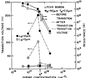
250 - - i . . ~ l l J IOI~ 0 " ~ 0 ~ 1 1 " ~ - LPCVD BORON _ 109 ~ E ~ I I WR = 50/J,m TR = 0.2/J.m - - BEFORE _ 2O0 IO s / / ! ~ TRANSITION /' ! ~\-'z-" .... AFTER I07 "' / t ( - ~ TRANSITION (~ C9 < 150 .' t \ \ - - - TRANSITION lOS uJ > j ', ~ VOLTAGE (,.) \ 105 z z 9 . . . '\ ~-
0 I00 9 LR=IOF. m "'~IB, '\ r
t ~' ' L U r- ~ LR=5~,m
/'~ f'-%~
,04 z I03 <c n / i ~ I \ = -;," ... o---J--I ~-- I0 2 5 0 0 ~ I | I 0 i 0 . . . 0 0 I I I 100 1016 i017 ,,!'~ 1018 1019 DOPING CONCENTRATION (cm -5)Fig. 2. Transition voltage and resistance vs. (loping level before end offer switching (power ~< O.5W).
) unless CC License in place (see abstract). ecsdl.org/site/terms_use
address. Redistribution subject to ECS terms of use (see 140.113.38.11
Vol. 132, No. 5
P O L Y C R Y S T A L L I N E SILICON F I L M R E S I S T O R S
1195
2 5 O F ' ~ , , ~ i
i
1 m,o/ r'l"-r.1 ~ l l LPCVD BORON
~ E ~ WR = 50ju.m TR'O.Zp-m toe
^ 2 o o - - B E F O R E
.."~ ~
TRANSmON lOS
_ _ / L ~ \ .... AFTER I0 7 / i \ \ TRANSITION 150/"
i i "~ ---TRANSITION I06 "~ 0 / ~ B VOLTAGE 0 > 9 IO 5 z 9 LR=lO/~m ~' 0 f-I L R= 5/J.m \ ~- too /I o \ 1o 4 ,,, z / i \ E ,~ - - / , \ io 3 i,- / / I I025o
o
t I b . . . m' . . . , ,oo 1016 i017 !* 1018 1019 DOPING CONCENTRATION (cm -3)Fig. 3. Transition voltage and resistance vs. doping level before and after switching (power ~< 2 . 2 W ) .
empirical expression
Iv = Io[exp
(VJVT)]
where lo and Vo are empirical parameters.D i s c u s s i o n
A simple qualitative model is proposed to u n d e r s t a n d the above observations. When the applied voltage is be- low the transition voltage, the I-V characteristics of polysilicon resistor can be described by the carrier trapping a n d dopant-segregation models (9-13). According to these models, the active d o p a n t concentration can be obtained by subtracting the inactive segregated d o p a n t concentration from the actual doping concentration (10, 11), and the grain-boundary trapping states can trap free carriers from the ionized active d o p a n t s a n d act as recom- bination centers (14, 15). This trapping process reduces the n u m b e r of free carriers and creates built-in potential barriers s u r r o u n d i n g the grain boundary, which i m p e d e carrier motion from one crystallite to another. The carrier transport across the grain b o u n d a r y a n d the built-in po- tential barriers by thermionic emission a n d t u n n e l i n g processes show a hyperbolic sine function I-V character- istic (13).
As the applied voltage further increases, the forward- biased space-charge barrier can eventually be flattened
108 cl 107 P _~ 106 oc I05 r ZPCVDIARsEINJC I 1012 F L R= IO/J'm WR = 50/r m II / A \ 9 N= hdOlTcm-:5 I0 i-- ~ A 9 -3
,e,OL
'+\
109 ~ A BEFORE TRANSITION 104 . . . AFTER TRANSITION103
///"
""',%
10 2 ," " 9 i- ... a I01 I I I I "'-A I 0.0 O. 2 0.4 0.6 0.8 1.0 1.2 FILM THICKNESS (/rFig. 4. Resistance vs. film thickness before and after switching
250 i i i i . o o LR= lO~m A 9 N = ix IOItcm "s 150 X A N=ZxlOIScrn -3 IOO X A 0 I I I I I 0.0 0.2 0.4 0.6 0.8 1.0 1.2 FILM THICKNESS (p.rn)
Fig, 5. Transition voltage vs. film thickness
and a great n u m b e r of carriers is then injected into the re- sistors. Once this happens, bulk resistance of silicon crys- tallite becomes dominant, and the I-V characteristic ex- hibits a transition from "grain-boundary limited" to "bulk-limited" condition. Thus the observation that tran- sition voltage reaches a m a x i m u m value around the criti- cal doping concentration can be understood by the fact that the highest built-in potential barrier exists at this doping concentration (10) and, therefore, a higher voltage is needed to flatten the forward-biased built-in potential barrier.
For lightly doped polysilicon films, the crystallites are totally depleted by the grain-boundary trapping states, a n d hence the films are nearly intrinsic. The resistivity of totally depleted polysilicon films is very high, a n d this semi-insulating property is m a i n l y due to carrier deple- tion rather t h a n mobility degradation (10). If a finite volt- age which is large enough to flatten the built-in potential barrier is applied across the resistor, a large n u m b e r of electrons a n d holes can be injected at the cathode a n d the anode, respectively. Because there are more u n f i l l e d grain-boundary traps for capturing minority carriers t h a n for majority carriers, the lifetime of minority carriers is shorter.
If the resistor is long compared to the m e a n free path of minority carriers, the minority carriers are not able to transverse the resistor, a n d this condition results i n single injection. U n d e r a high current level, majority-carrier single injection is space-charge limited (16). However, as the bias is further increased, the field across the resistor eventually becomes high enough to allow the minority
i t I I r I l LPCVD BORON ] LR=IOp'm, WR=5Op'm I N = 2xlO 18 cm "3 I @AWlTH CONTACT A.J40
60
'o o~wiT.OUT CONTACT / " t
30 i- < 40 z0
e..
z 30 20 o./,./,
zo
aoE
-tO v- I0 P I I I 0.0 0.2 0.4 0,6 0.8 1.0 1,2 FILM THICKNESS (/zm)Fig. 6. Transition voltage and transition current vs. film thickness
) unless CC License in place (see abstract). ecsdl.org/site/terms_use
address. Redistribution subject to ECS terms of use (see 140.113.38.11
1196 J. E l e c t r o c h e m . Soc.: S O L I D - S T A T E S C I E N C E A N D T E C H N O L O G Y M a y 1985 carriers to reach the other end of the resistor. This double
injection process causes the majority space-charge barrier to be lowered and minority carrier lifetime (mobility) to increase, p e r m i t t i n g m o r e carriers to transit the resistor; as a result, a lower voltage is required to provide the cur- rent for maintaining the condition. This positive feedback process results in negative resistance characteristics. The condition causing this negative resistance behavior is that the minority carrier transit time is equal to their lifetime. It is clear that in a shorter resistor it is easier to reach this condition. Eventually, the high level injection condition will be reached w h e n the lifetimes of minority and major- ity carriers are equal. A t this point, two-carrier recombi- nation-limited current flow prevails and the negative re- sistance behavior terminates; the polysilicon resistor can then switch to the " o n " state. This double injection mode is m u c h more likely observed for small grain and/or lightly doped polysilicon films w h i c h have plenty of recombination centers for both majority and minority car- riers (17).
Similar p h e n o m e n a have b e e n observed in m a n y amorphous semiconductors w h e r e the initiation of switching and the maintenance of the "on" state in threshold switching can be satisfactorily explained as a double injection electronic process (18, 19). U n d o p e d or lightly doped polysilicon films of small grain size have m a n y properties close to a m o r p h o u s films. J u s t like any electronic transport process, heat will be generated by current, and thermal effects will a c c o m p a n y this elec- tronic injection process. For short polysilicon resistors, however, the high field induced carrier generation is more likely to occur before thermal effects take over the major role. Therefore, if the d o u b l e injection process and positive feedback m e c h a n i s m occur before J o u l e heating makes any microstructure change, a reversible threshold switching occurs. However, if m o r e p o w e r is fed into the "on" state resistor, the J o u l e heating will finally b e c o m e large enough to cause an irreversible switching from " o n " state to "short" or " o p e n " state.
For heavily d o p e d polysilicon films, although the grain-boundary trapping states are completely filled up with majority carriers, the concentration of free majority carriers is still substantially larger than the intrinsic car- rier concentration and of the same order of m a g n i t u d e as the active doping concentration (10, 11). The lifetime of minority carrier is m u c h shorter than that of majority car- rier. This majority carrier transport process is not space- charge limited. The double injection condition is hardly reached even u n d e r a relatively large bias. Usually, the thermal process will t h e n prevail to induce current filamentation (20). Thermal current filamentation results in irreversible switching to either "short" or " o p e n " state, depending on the configuration of resistor and program- ming conditions. F o r thick and short resistors, thermal filamentation can induce either dopant migration or alu- m i n u m penetration through the molten filament to form "short" state (1). For thin and long resistors, J o u l e heating can simply evaporate the polysilicon film to leave a void (21), or the applied field can be strong enough to sweep the molten silicon ions to form an " o p e n " gap (1).
It should be noted that the coexistent electronic and thermal processes always c o m p e t e and influence each other. Therefore, the device configuration, composition of the resistor, and the p r o g r a m m i n g conditions all have their roles and b e c o m e a control parameter in some par- ticular stage of this c o m p l e x switching p h e n o m e n o n .
Conclusion
Several distinct patterns of polysilicon resistance switching have been observed for both arsenic- and
boron-doped materials over a wide range of doping con- centration and film thickness. The transition voltage reaches a m a x i m u m value around the critical doping con- centration, which separates the totally d e p l e t e d and par- tially depleted cases. B e y o n d this point, toward higher doping levels, the transition voltage generally follows the variation of Rb. As applied p o w e r increases, resistance after switching to "short" state can be further decreased and becomes less d e p e n d e n t on film thickness and dop- ing level and, finally, a l u m i n u m penetration occurs, caus- ing a resistance of only a few ohms.
Lightly doped resistors are more likely to show revers- ible threshold switching, probably due to their abundant recombination centers. Short and thick resistors are more likely to switch to "short" state, and the a l u m i n u m pene- tration path can be easily observed. L o n g and thin resis- tors are more likely to switch to " o p e n " state, and a phys- ical gap is observed. These distinct patterns have been understood by a qualitative model.
Acknowledgments
The authors wish to thank Dr. Ming-Kwang Lee of ERSO, Industrial Technology Research Institute, ROC, for sample preparation, and Professor Si-Chen Lee of Na- tional Taiwan University for many valuable discussions. C. Y. Lu wishes to thank Dr. A. R e i s m a n for his encour- agement and support during his stay in N C S U and MCNC. We also would like to t h a n k Dr. L. M. Terman for helpful c o m m e n t s and C. Winston for typing this paper.
Manuscript submitted J u n e 11, 1984; revised manu- script received Dec. 7, 1984.
IBM Corporation assisted in meeting the publication costs of this article.
R E F E R E N C E S
1. D. W. Greve, IEEE Trans. Electron Devices, ed-29, 719 (1982).
2. J. E. Mahan, Appl. Phys. Lett., 41, 479 (1982).
3. M. Tanimoto, J. Murota, Y. Ohmori, and N. Ieda, IEEE Trans. ELectron Devices, ed-27,517 (1980).
4. R. K. Wallace, ISSCC Dig. Tech. Papers, 148 (1980). 5. L. R. Metzger, IEEE J. Solid-State Circuits, sc-18, 562
(1983).
6. T. Mano, K. Takeya, T. Watanabe, N. Ieda, K. Kiuchi, E. Arai, T. Ogawa, and K. Hirata, ibid., sc-15, 865 (1980). 7. D. W. G r e v e and L. V. Trans, IEEE Trans. Electron De-
vices, ed-29, 1313 (1982).
8. M. E. L u n n o n and D. W. Greve, J. Appl. Phys., 54, 3270 (1983).
9. G. J. Korsh and R. S. Muller, Solid-State Electron., ~1, 1045 (1978).
10. N. C. C. Lu, L. Gerzberg, C. Y. Lu, and J. D. Meindl, IEEE Trans. Electron Devices, ed-28, 818 (1981). 11. M. M. Mandurah, K. C. Saraswat, C. R. Helms, and T. I.
Kamins, J. Appl. Phys., 51, 5755 (1980).
12. N. C. C. Lu, C. Y. Lu, M+ K. Lee, C. C. Shih, C. S. Wang, W. Reuter, and T. T. Sheng, This Journal, 131, 897 (1984).
N. C. C. Lu, L. Gerzberg, C. Y. Lu, and J. D. Meindl, IEEE Trans. Electron Devices, ed-30, 137 (1983). H. C. Card and E. S. Yang, ibid., ed-24, 397 (1977). W. Hwang, E. Poon, and H. C. Card, Solid-State Elec-
tron., 26, 599 (1983).
M. A. L a m p e r t and P. Mark, " C u r r e n t Injection in Sol- ids," A c a d e m i c Press, New York (1970).
M. Braustein, A. I. Braustein, and R. Zuleeg, Appl. Phys. Lett., 10, 313 (1967).
D. Adler, M. S. Shur, M. Silver, and S. R. Ovshinsky, J. Appt. Phys., 51, 3289 (1980).
D. Adler, H. K. Henisch, and N. Mott, Rev. Mod. Phys., 50, 209 (1978).
D. H. Pontius, W. B. Smith, and P. P. Budenstein, J. Appl. Phys., 44, 331 (1973).
R. J. Smith, IEEE IEDM Tech. Dig., 608 (1982). 13. 14. 15. 16. 17. 18. 19. 20. 21.
) unless CC License in place (see abstract). ecsdl.org/site/terms_use
address. Redistribution subject to ECS terms of use (see 140.113.38.11