探討電極緩衝層的摻雜效應對有機太陽能電池效率之研究
71
0
0
全文
(2) 研究成果 (A) 期刊論文(Journal) 1. Chien-Jung Huang, Kan-Lin Chen, Yao-Jen Tsao, Dei-Wei Chou, Wen-Ray Chen, and Teen-Hang Meen, “Study of solvent-doped PEDOT: PSS layer on small molecule organic solar cells”, Submitted to Current applied Physics, April 2012.. 2. Dei-Wei Chou, Kan-Lin Chen, Chien-Jung Huang, Yao-Jen Tsao, , Wen-Ray Chen, and Teen-Hang Meen, “Efficient small molecule organic solar cells incorporating doped buffer layer”, Submitted to Thin Solid Films, July 2012.. (B) 研討會論文(Conference) 1. Chien-jung Hauang, Yao-Jen Tsao, Jhong-Ciao Ke, Dei-Wei Chou, Wen-Ray Chen, and Teen-Hang Meen, “Sorbitol addition of the PEDOT:PSS films enhanced efficiency on the small molecule organic solar cell”, Submitted to Nanotechnology and Printed Electronics Symposium 2011 in Singapore (July 4-5, 2011), Apr. 12, 2011, p.76. (C) 專利 1. 黃建榮,曹耀仁,“聚乙烯二氧噻吩-聚苯乙烯磺酸鹽導電液及由其所形成的導 電膜”中華民國專利,申請中.. I.
(3) Investigation of the doping effect in electrode buffer layers for the efficiency of organic solar cells Advisor(s): Dr. Chien-Jung Huang Institute of Applied Physics National University of Kaohsiung Student: Yao -Jen Tsao Institute of Applied Physics National University of Kaohsiung. ABSTRACT In this study, small molecule organic solar cell with an optimized structure of ITO/ CuPc 10nm/ CuPc:C60 (20nm)/ C60 (20nm)/ BPhen (5nm)/ Ag was fabricated. We incorporated the PEDOT:PSS layer as the anode buffer layer between ITO anode and CuPc layer. We try improving the property of PEDOT: PSS layer by addition of solvent, such as such as sorbitol, glycerol and DMSO. With 3wt% sorbitol-doped PEDOT: PSS layer as the anode buffer layer, the short-circuit current density (Jsc) increased from 5.11 mA/cm2 to 15.45 mA/cm2, the open-circuit voltage (Voc) increased from 0.47 to 0.51 V, and the power conversion efficiency (ηp) increased from 1.28 to 3.37% under 100mW/cm2 AM1.5G illumination. These improvements were attributed to reach the optimal balance among the the carrier collection efficiency, light absorption efficiency, and transmittance of the device. In addition, 3wt% sorbitol-doped PEDOT: PSS layer has been used as buffer layer between CuPc layer and ITO which causes the good contact with the anode. Thus, the incorporation of 3wt% sorbitol-doped PEDOT: PSS layer results in enhancement of Jsc and performance of the device. Based on the optimal structure, we improved BPhen layer doped with Cs2CO3 as cathode buffer layer between the C60 layer and Ag cathode to accelerate the transport of. II.
(4) electrons. The small molecule organic solar cell with structure of ITO/ PEDOT: PSS (doped with 3wt% sorbitol) / CuPc (10nm)/ CuPc: C60 mixed (20nm)/ C60 (20nm)/ Cs2CO3:BPhen (1:4) (5nm)/ Ag. The cell with Cs2 CO3: BPhen (1:4) layers exhibits power conversion efficiency (PCE) of 3.51% as compared to 3.37% for the device with pristine BPhen layer. The enhanceded PCE in cell was considered as favorable energy level alignment between Cs2CO3: BPhen layer and the fullerene (C60) layer. In addition, the surface morphology is improved by adding Cs2 CO3 to BPhen layer.. Key words: organic solar cell, power conversion efficiency, PEDOT: PSS. III.
(5) 探討電極緩衝層的摻雜效應對有機太陽能電池效率之研究 指導教授:黃建榮博士 國立高雄大學應用物理系 學生:曹耀仁 國立高雄大學應用物理系. 摘要 在本研究中,從已最佳化厚度的結構 ITO/ CuPc 10nm/ CuPc:C60 (20nm)/ C60 (20nm)/ BPhen (5nm)/ Ag 加入陽極緩衝層 PEDOT:PSS 至 ITO 與 CuPc 之間,並藉由 摻雜溶劑改善陽極緩衝層 PEDOT:PSS,總共嘗試了三種溶劑,分別為山梨醣醇、甘 油和 DMSO,使得短路電流從 5.11 mA/cm2 上升到 15.45 mA/cm2,開路電壓從 0.47V 上升到 0.51V,轉換效率從 1.28%上升到 3.37%在 AM1.5G 的太陽能光譜下。這些增 加是歸因於在載子的收集效率、光的吸收效率達到最佳化,此外,使用摻雜 3wt%的 山梨醣醇的 PEDOT:PSS 當作陽極緩衝層,能夠導致陽極與主動層接觸更好,使得元 件的短路電流及效率獲得大幅改善。 為了更進一步改善元件的效率,我們在陰極緩衝層 BPhen 摻雜碳酸銫,結構為 ITO/ PEDOT: PSS (doped with 3wt% sorbitol) / CuPc (10nm)/ CuPc:C60 (20nm)/ C60 (20nm)/ Cs2CO3:BPhen (1:4) (5nm)/ Ag,在此結構下元件效率獲得改善,從未摻雜碳酸銫之元 件 3.37%上升至 3.51%,改善的原因為摻雜碳酸銫後 BPhen 層能階的變化和表面形貌 的改善。 關鍵字:有機太陽能電池、轉換效率、聚二氧乙基噻吩-聚苯乙烯磺酸複合物 IV.
(6) Contents Chapter 1 Introduction-------------------------------------------------------------------------1 1-1 This history of solar cell-------------------------------------------------------------------1 1-2 The history of organic solar cell----------------------------------------------------------2. Chapter 2 Theory of solar cell---------------------------------------------------------------6 2-1 Solar spectrum-----------------------------------------------------------------------------6 2-2 Working principle of solar cells----------------------------------------------------------8 2-2-1 Light absorption-----------------------------------------------------------------------8 2-2-2 Charge separation----------------------------------------------------------------------8 2-2-3 Charge transport-----------------------------------------------------------------------8 2-3 Performance analysis----------------------------------------------------------------------8 2-3-1 Dark current and photocurrent-------------------------------------------------------9 2-3-2 Voc and FF and PCE-----------------------------------------------------------------10 2-3-3 Shunt resistance (Rsh) and series resistance (Rs)--------------------------------11 2-3-4 The quantum efficiency and spectral response-----------------------------------12 2-3-5 Temperature effect-------------------------------------------------------------------13 2-3-6 Limits to solar cell conversion efficiency-----------------------------------------14 2-4 Principle of operation and devices concept-------------------------------------------15 2-4-1 Homojunctions-----------------------------------------------------------------------15 2-4-2 Heterojunction------------------------------------------------------------------------17 2-4-3 Dispersed Heterojunction-----------------------------------------------------------17 2-4-4 Organic solar cell materials---------------------------------------------------------18. Chapter 3 Experiment procedure--------------------------------------------------------21 3-1 The etching and cleaning of ITO substrate-------------------------------------------21 3-2 Deposition of organic thin films and electrode---------------------------------------22 V.
(7) 3-3 Measurements----------------------------------------------------------------------------22. Chapter 4 Results and discussion---------------------------------------------------------24 4-1 The insertion of the solvent-doped PEDOT:PSS layer as the anode buffer layer -------------------------------------------------------------------------------------------24 4-2 The sheet resistance and morphology of solvent-doped PEDOT:PSS layer ---------------------------------------------------------------------------------------------25 4-3 The transmittance of various doped anode buffer layers----------------------------26 4-4 The EQE spectrum of the devices with various doped anode buffer layers ---------------------------------------------------------------------------------------------26 4-5 The improvement of cathode buffer layer by addition of Cs2CO3 -----------------------------------------------------------------------------------------------27 4-6 The characteristics of devices incorporating Cs2CO3:BPhen layer with different ratios and the device with pristine BPhen layer ----------------------------------------28 4-7 The analysis of the morphology and optics of the devices incorporating Cs2CO3:BPhen layer with different ratios and the device with pristine BPhen layer -------------------------------------------------------------------------------------------------29. Chapter 5 Conclusion and Future work-----------------------------------------------33 5-1 Conclusion--------------------------------------------------------------------------------32 5-2 Future work-------------------------------------------------------------------------------33. References------------------------------------------------------------------------------------------34. VI.
(8) Figure captions Figure 1.1 Oil prices, 1861-2006-------------------------------------------------------------------37 Figure 2.1 Solar spectrum---------------------------------------------------------------------------38 Figure 2.2 The equivalent circuit of a solar cell--------------------------------------------------39 Figure 2.3 I-V characteristics of solar cell--------------------------------------------------------40 Figure 2.4 The equivalent circuit of solar cell with Rs and Rsh-------------------------------41 Figure 2.5 Plots of the equation for various combinations of the series and shunt resistance---------------------------------------------------------------------------------42 Figure 2.6 Schematic energy-band diagram of a simple device consisting of single organic layer between two metal contacts-----------------------------------------------------43 Figure 2.7 Schematic of energy-band diagram of a donor-acceptor heterojunction--------------------------------------------------------------------------44 Figure 2.8 A blend of two polymers---------------------------------------------------------------45 Figure 2.9 A blend of one polymer with electron accepting nanoparticles or fullerene----------------------------------------------------------------------------------46 Figure 4.1 Schematic structure of the organic photovoltaic cells------------------------------47 Figure 4.2 Schematic energy levels of the device------------------------------------------------48 Figure 4.3 Comparison of the sheet resistance and surface roughness with various (a) sorbitol-doped (b) glycerol-doped (c) DMSO-doped PEDOT: PSS concentrations on the ITO-glass substrate------------------------------------------49 Figure 4.4 The transmittance of different doped PEDOT: PSS with optimal concentration on the ITO-glass substrate -----------------------------------------------------------50 Figure 4.5 The EQE of different doped PEDOT: PSS with optimal concentration on the ITO-glass substrate--------------------------------------------------------------------51 Figure 4.6 (a) Schematic structure of the organic photovoltaic cells and (b) schematic. VII.
(9) energy levels of the device ----------------------------------------------------------52 Figure 4.7 J-V characteristics of the small molecule organic solar cells with different cathode buffer layers --------------------------------------------------------------53 Figure 4.8 AFM images of the (a) pristine BPhen, (b) Cs2CO3:BPhen (1:4), (c) Cs2CO3:BPhen (2:4), (d) Cs2CO3:BPhen (4:4) layer evaporated on the ITO/ PEDOT:PSS/ CuPc/ CuPc:C60/ C60----------------------------------------------------54 Figure 4.9 The absorption spectra of pristine BPhen and Cs2CO3:BPhen(1:4) layer ------55 Figure 4.10 The EQE of the device with BPhen layer and the device with s2CO3:BPhen(1:4) layer --------------56. Table captions Table 1.1 Efficiency of solar cells-----------------------------------------------------------------57 Table 2.1 Integrated Solar Energy Received Annually in Various Countries---------------58 Table 4.1 Photovoltaic performance parameters of different devices ------------------------59 Table 4.2 The conductivity of PEDOT: PSS layers doped with different sorbitol concentrations --------------------------------------------------------------------------60 Table 4.3 The current-voltage characteristics of the devices with different cathode buffer layers -------------------------------------------------------------------------------------61. VIII.
(10) 第一章 緒論 有機太陽能電池(Organic solar cells, OSC)具有可輕量化、厚度薄、可大面積製 作、製作成本低廉、製程簡單等優點。相較於目前市面上的無機太陽能太陽能 (Inorganic solar cells),有機太陽能電池擁有許多製程上的優勢。除此之外,有機太陽 能電池還有可撓性的特性,在應用上範圍更加寬廣,所以有機太陽能電池有相當大的 發展潛力。. 至從第一次石油危機,才讓人類開始重視到能源的重要。此時,太陽能電池才 被廣泛的研究。第一個有機太陽能電池被發表在期刊文獻是從 1985 年,由美國柯達 公司 Tang 等人,利用熱蒸鍍方法將小分子有機材料製作成雙層元件,但是效率非常 的低。如何提高有機太陽能電池的功率轉換效率是目前重要的課題。. 本論文共分為五章節,第一章為緒論;第二章為太陽能電池的理論和工作機制; 第三章包含實驗的步驟,製作方法以及量測儀器;第四章則是不同參數下有機太陽能 電池的實驗結果與討論;第五章為本論文的結論與未來研究方向。. 1.
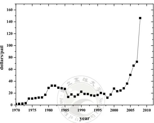
(11) Chapter 1 Introduction 1-1 The history of solar cell Solar cells have gradually played an important role in the world’s renewable energy market because fossil fuels are being exhausted and environmental protection. In recent years, the oil prices were increasing in Figure 1.1. It was also believed that the oil in the world would be finished. Scientists tended to search for new energy resources to replace oil, including Wind, Hydrogen, Biomass and Geothermal. Until now, solar energy was found the most common renewable energy resource [1]. Solar photovoltaic energy conversion is a one-step conversion process which generates electrical energy conversion from light energy. Light is made up of packets of energy, called photons, whose energy depends only upon the frequency of the light. The energy of visible photons is sufficient to excite electrons, up to higher energy levels where they are more free to move. Solar cells use the photovoltaic effect for their operations, which was shown on an electrode in an electrolyte solution. A similar effect was reported in solid selenium materials in 1877 by Adams and Day. This effect shows that showed a significant light dependent voltage between two contacts were selenium. The selenium solar cells had arrived about 1 % efficiency from directly converting sunlight into DC electricity in 1914. Technological development begins with the development of a diffused silicon p-n junction in 1954. Reynolds group described an efficiency of 6% by a copper sulfide/cadmium sulfide cell. Hence it is was estimated production cost of some$200 per Watt. Therefore, the early silicon solar cell can not used as resource [2]. Until now, the solar cells should be divided into three generations. The first generation solar cells can manufacture in large-area, single layer p-n junction diode. Nevertheless, the. 2.
(12) second solar cell was designed on buildings. Each active layer can absorb wavelength of light successively longer. The third solar cell was a new devices, including dye sensitized solar cells (DSSC), organic solar cell (OSC) and quantum dot solar cells. The development of different generation solar cells was demonstrated in Table 1.1. Organic solar cells have many attractive features, amongst them [1][3] (1) The potential to be flexible and semitransparent. (2) Potential to be manufactured in a continuous printing process. (3) Large area coating. (4) Easy integration in different devices. (5) Significant cost reduction compared to traditional solutions. (6) Substantial ecological and economic advantages.. 1-2 The history of organic solar cell (OSC) In recent years, it has seen an unprecedented growth of interest in solar cells made from organic electronic materials. This is due partly to the rapid growth of the photovoltaic market, which has stimulated research into longer term, more innovative photovoltaic technologies and partly to the development of organic electronic materials for display applications. Rapid progress in optoelectronic molecular materials has introduced a range of potential new photovoltaic materials as well as an improved understanding of the capabilities of such materials and confidence in their applications [4]. Organic materials are attractive for photovoltaic primarily through the prospect of high throughput manufacture using processes such as reel-to-reel deposition. Additional attractive features are the possibilities for ultra thin, flexible devices which many be integrated into appliances or building materials and tuning of colour through chemical structure. The field has made impressive progress since the late 1990s. At the time of 3.
(13) writing, solar power conversion efficiencies of over 3 % have been reported for four distinct classes of organic solar cell, a growing range of new photovoltaic materials have been studied and increasing numbers of research groups and companies have declared an interest in soft solar cells [5-7]. The power conversion efficiency (PCE) approaching 5% was reported by several groups for organic solar cells based on single layer of polymer bulk heterojunction, which is a blend of electron donor and electron acceptor. Although much effort has been made to improve the device performance, including thermal treatment [8-9], film thicknesses [9-10], change in active materials, light harvesting structure…etc. Besides, the experimental studies many theoretical researches was conducted to explore the limitations of the device performance of BHJ solar cells [9, 11]. Many conditions in the theoretical calculation were studied such as carrier mobility, energy level position and band gap. The PCE of organic solar cells was predicted to be more than 10% ultimately [11-13]. One of the key factors to demonstrated PCE is the open-circuit voltage (Voc). It is hard not only to control the Voc but also to understand the relation among Voc, electrodes and bulk energy levels to date. For the commonly studied small molecule organic solar cells with Copper phthalocyanine (CuPc) as a electron donor and fullerene (C60) as electron acceptor the energy difference is 0.7eV. However, Voc of organic solar cells is only about 0.5V experimentally. Furthermore, many experiments show that Voc is rather than insensitive to the type of the metal electrodes [9, 14]. Besides, the value of open-circuit voltage (Voc) is by the energy difference between highest occupied molecular orbital (HOMO) of donor and lowest unoccupied molecular orbital (LUMO) of acceptor [15]. And then there are improvement methods of OSC from introduction of devices concept such as changes in active materials, light harvesting structure, annealing [16], and the electron transport layer (ETL) [17]. Among these, the use of ETL has been widely. 4.
(14) investigated [18-19]. For example, Forrest et al. has shown that introducing bathocuproine (BCP) between fullerene (C60) and aluminum (Al) cathode based on a copper phthalocynine (CuPc)/ C60 heterojunction, is critical in promoting efficiency of OSC [17]. The authors found that when no ETL material is present, the resulting OSC has a poor PCE. Reasons for a poor PCE are thought to include: (1)during Al deposition processing, the Al atom diffuse to C60 layer [20], causing in low conductivity of C60 (2) a covalent bond is formed between C60 and Al, resulting in inefficient electron collection between C60 and Al [21].. 5.
(15) 第二章 有機太陽能電池的工作機制和理論 然而,太陽能光譜中的可見光部份佔整個太陽能光譜有 80 %以上。所以選用的 主動層材料必須能吸收到可見光的部分。當有機材料吸收到太陽光時,則會產生電子 -電洞對。而則些電子-電洞對必須擴散至接面產生分離,再藉由陰陽極的功函數差將 電洞往陽極輸出,則電子往陰極輸出到達外部。在有機太陽能電池結構中,各個有機 材料都有各自的功能存在,包含能階的匹配、材料的吸收率都是必須考量的項目。此 外靠近陰極的有機材料的選擇,在有機太陽能電池中扮演一個很重要的角色。如何增 加電子輸出至外部的量,是有機太陽能電池具有較高的功率轉換效率不可或缺的課 題。. 在太陽能電池中,有幾個重要參數是必須知道的。如:光電流(Jsc)、開路電壓 (Voc)、填充因素(FF)、功率轉換效率(PCE)、串聯電阻(Rs)、並聯電阻(Rsh),而這些 參數之間都是有關係存在的,都會去影響到有機太陽能電池的功率轉換效率。然而, 光電流主要是受到串聯電阻所影響,太陽能電池的串聯電阻主要有幾個原因:由表面 與電極之電阻(2)電極和半導體接面之歐姆接觸(3)材料本身的電阻。並聯電阻則有: (1)內部復合電流(2)表面複合電流(3)元件的邊緣未隔離。所以一個理想太陽能電池所 具備必須是低串聯電阻和高並聯電阻。. 有機太陽能電池的結構的形式有 Homojunctions、Heterojunction、Dispersed heterojunction,此三種方法都有各自的優缺點及改進的方法。而本實驗室是採用 Heterojunction 結構再加上電子傳輸層以及使用複合陰極來改善有機太陽能電池的功 率轉換效率。. 6.
(16) Chapter 2 Theory of solar cell 2-1 Solar spectrum The spectral distribution of the radiation emitted from the sun is determined by the temperature of the surface of the sun, which is about 6000K. The wavelength distribution of the sunlight (power per unit area and per unit wavelength) follows approximately the radiation distribution of a black body at this temperature, as can be seen in Figure 2.1. The deviations at certain wavelengths are due to absorption effects in the sun atmosphere. For the comparison of the conversion efficiency of different solar cells, the knowledge of the exact spectral distribution is important, since they can respond differently to different wavelengths. The total energy per unit area integrated over the entire spectrum and measured outside the atmosphere perpendicular to the direction of the sun is essentially constant. This radiation power is referred to as the solar constant or air mass zero (AM0) radiation. Measurements taken at high altitudes have yielded the currently accepted average value of 1.353 kW/m2 [22-23]. The spectral distribution is changed considerably when the sunlight penetrates through the earth’s atmosphere. Even for a clear sky the light intensity is attenuated by at 30 % because of scattering at molecules, aerosols and dust particles, and absorption by the atmosphere’s constituent gases, such as water vapor, ozone, or carbon monoxide. The attenuation mechanisms are wavelength-dependent, which explains the strong absorption bonds in the spectral distribution measured at the earth’s surface [24-26]. The measurement of the radiant power is further complicated by the fact that the degree of attenuation is highly variable because of the constantly changing position of the sun and the corresponding change of the light path through the atmosphere. The ratio of the actual. 7.
(17) path length to its minimum value has been defined when the sun is directly overhead as optical air mass and the corresponding radiation as air mass one (AM1) radiation. For any given angle θ with respect to the overhead position, the atmospheric path h relative to the minimum path length h0 when the sun is directly overhead is given by h ho / cos . The optical air mass is thus increased by the factor m 1 / cos and takes the value AM m . It is evident that terrestrial sunlight varies greatly both in intensity and spectral distribution. Therefore it became necessary to define a terrestrial standard that allows a meaningful comparison of different solar cells tested at different locations. In the U.S photovoltaic program, the spectral distribution for an AM 1.5 radiation with a total power density of 0.844 kW/m2 (for θ= 45 deg) has been adopted as a standard. Tabulated values of the spectral distribution are given in [26] and refer to sunlight in a cloudless sky.. The. AM1 spectrum is for an angle of 0 deg and has an incident power of about 0.925 kW/m2. The solar spectrum has contributions from direct and diffuse sunlight. The diffusive component can account for about 20 % of the total radiation in a clear sky, but this fraction can increase considerably with the cloud coverage and the position of the sun. For instance, the mean daily global irradiation is sunny locations in Europe ranges from 3.2 to 5.2 kW/m2 [25]. Since the spectral distribution for diffuse radiation is different from direct sunlight, there exists a great variability both in the intensity and the spectral composition at different locations on the earth (Table 2.1) [27].. 2-2 Working principle of solar cells [28] 2-2-1 Light absorption High absorption of light with E > Eg is straightforward to achieve in principle. Increasing the thickness of the absorbing layer increases its optical depth, and for most semiconductors almost perfect absorption can be achieved with a layer a few tens or 8.
(18) hundreds of microns thick. However, the requirements of high optical depth and prefect charge collection make very high demands of materials quality.. 2-2-2 Charge separation For a current to be delivered, the materials should be contacted in such a way that the promoted electrons experience a spatial asymmetry, which drives them away from the point of promotion. This can be an electric field, or a gradient in electron density. This asymmetry can be provided by preparing by preparing a junction at or beneath the surface. The junction may be an interface between two electronically different materials or between layers of the same materials treated in different ways.. 2-2-3 Charge transport To conduct the charge to the external circuit the materials should be a good electrical conductor. Perfect conduction means that carriers must not recombine with defects or impurities, and should not give up energy to the medium. There should be no resistive loss or current leakage. The materials around the junction should be highly conducting and make good Ohmic contacts to the external circuit. Mechanisms for excitation, charge separation and transport can be provided by the semiconductor p-n junction, which is the classical model of a solar cell. In this system charge separation is achieved by a charged junction between layers of semiconductor of different electronic properties. The driving force which separates the charges is electrostatic.. 9.
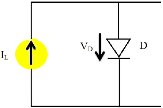
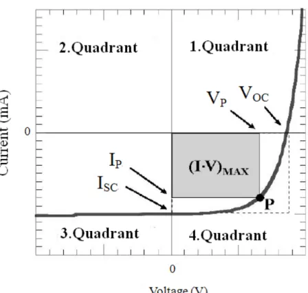
(19) 2-3 Performance analysis 2-3-1 Dark current and photocurrent A solar cell is formed by a p-n diode. Since the solar cell is a diode, the Current-Voltage characteristics are given by J Jo(e qV. kBT. -1). where Jo is a constant, KB is Boltzmann’s constant and T is temperature in degrees Kelvin. Under illumination, the diode equation is modified as: I Io[e qV. AKT. -1]-IL. where IL is photocurrent which opposes the dark current of the diode and I is the net current through diode, parameter A is the diode ideality factor, k is Boltzmann’s constant, T is the temperature in Kelvin. The equivalent circuit of a solar cell in Figure 2.2 and corresponding I-V characteristicis shown in Figure 2.3.. 2-3-2 Open-circuit voltage (Voc) and Fill Factor (FF) and power conversion efficiency (PCE) Under illumination, the I-V curve shifts down to the fourth quadrant, as shown in Figure 2.3 The open-circuit voltage(Voc) can be solved by substituting I=0 and V=Voc from equation. Voc . kT Jsc ln( 1) q Jo. The Fill Factor (FF) is defined as the measure of squareness, which is expressed as: FF . Vp * Ip Voc * Isc. The efficiency η of the cell is the power density delivered at operating point as a fraction of the incident light power density Pin:. 10.
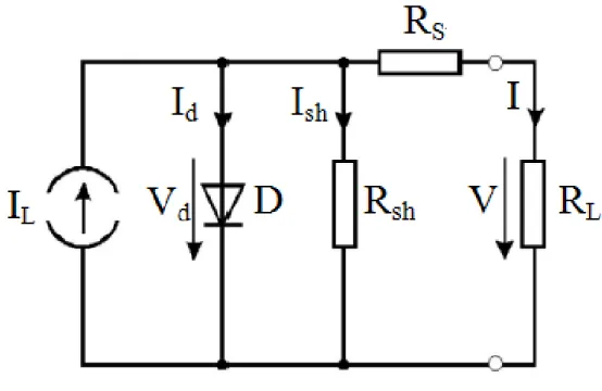
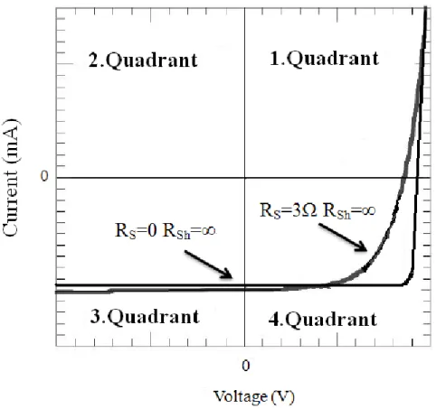
(20) . Ip *Vp Pin. Then, the efficiency can be expressed as:. . Jsc *Voc * FF Pin. These four quantities: Jsc, Voc, FF and η are key performance characteristics of a solar cell. All of these should be defined for particular illumination conditions. The Standard Test Condition (STC) for solar cells is the Air Mass 1.5 spectrum, all incident power density if 1000W/m2 and a temperature 25℃. 2-3-3 Shunt resistance (Rsh) and series resistance (Rs) When parasitic resistances are included, the solar cell equation becomes J Jsc Jo(e q(V JARs. kT. 1) . V JARs Rsh. These effects are equivalent electrically to two parasitic resistances in series (Rs) and in parallel resistance (Rsh) with the cell, as shown in Figure 2.4. The origin of the series resistance is the bulk resistance of the semiconductor and the resistance of the contacts and interconnections. The shunt resistance can be caused by extended lattice defects in the depleted region or leakage currents around the edges of the cell. Extended defects which can easily occur in low-cost semiconductors are dislocations, grain boundaries and large precipitates [29]. To evaluate the ramifications of these parameters on the current-voltage characteristics, one can describe the electric behavior of the non-ideal pn junction according to (2.46). Plots of the equation for various combinations of the series and shunt resistance in Figure 2.5 show that essentially the shape of the current-voltage characteristics and hence the FF is changed. The shunt resistance as low as 100Ω does not appreciably change the power output of the device, it can be seen that a small series. 11.
(21) resistance of only 5Ω reduces the total efficiency by 30 % already. For a typical silicon solar cell, the series resistance is about 0.7Ω.. 2-3-4 The quantum efficiency and spectral Response The quantum efficiency of a solar cell is defined as the ratio of the number of electrons in the external circuit produced by an incident photon of a given wavelength. Thus, one can define external and internal quantum efficiency. They differ in the treatment of photons reflected from the cell: all photons impinging on the cell surface are taken into account in the value of the EQE but only photons that are not reflected are considered in the value of IQE. If the internal quantum efficiency is known, the optical photo generated current is given by Iph q ( ) ( ){1 R ( )}IQE ( )d. where Φ(λ) is the photon flux incident on the cell at wavelength λ, R(λ) is the reflection coefficient from the top surface, and the integration is carried out over all wavelength λ of light absorbed by the solar cell. The values of the internal and external quantum efficiency are routinely measured to assess the performance of a solar cell by using interference filters or monochromators. The spectral response is defined as the ratio of the photocurrent generated by a solar cell under monochromatic illumination of a given wavelength, to the value of the spectral irradiance at the same wavelength. Since the number of photons and irradiance are related, the spectral response can be written in terms of the quantum efficiency as SR ( ) . q QE ( ) 0.808 * * QE ( ) hc. where λ is in micrometers. Spectral response in equation can be either internal or external, depending on which value is used for the quantum efficiency [30].. 12.
(22) 2-3-5 Temperature Effect A considerable fraction of the incident light is transformed into heat and the operating temperature of a solar cell can very over a wide range of temperature, especially in the case of concentrator cells. The material parameters, which mainly change with the temperature, are the band gap energy, which usually decreases and the minority lifetime, which generally increases with increasing temperature. This will increase the light generated current and thus Isc slightly due to the increased light absorption and the increase in minority-carrier diffusion length. However, the Voc will more rapidly decrease because of the exponential dependence of the saturation current on the temperature and correspondingly the FF will degrade. Therefore, the overall effect causes a reduction of the efficiency as the temperature increases. One can approximately estimate the change ΔVoc if one differentiates with respect to the temperature and considers only the significant terms:. Voc . eVoc KT E g 0 eT. T. Ego is the band gap at T= 0。K and γ is a parameter that summarizes the temperature dependence in the prefactors (~T-γ) of IL/Is and varies approximately between 1 and 4. Inserting appropriate values for silicon, the Voc decreases with temperature and the efficiency is reduced by about 0.5 % per 1℃ [31].. 2-3-6 Limits to solar cell conversion efficiency For any materials system, there are intrinsic limitations to photovoltaic energy conversion. These include open-circuit voltage and fill factor limitation. The value of Voc can never exceed the built-in voltage. If it did, the built-in field would be cancelled by the excess majority carriers on the two sides of the junction and excess minority carriers in the 13.
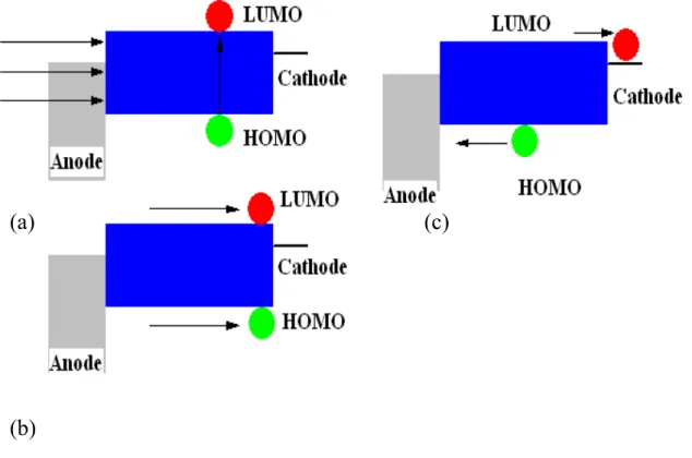
(23) quasi-neutral regions could no longer be separated. With regards to the fill factor, by referring to the cell I-V characteristics, it is seen that only the area in the rectangle bounded by Voc and Isc contributes to the power delivered to the load. The remaining power between the curve and the rectangle is lost through series and shunt resistances. The ideal cell would include zero series resistance and infinite shunt resistance in the equivalent-circuit model. Next, there is the limitation imposed by the mismatch between the magnitude of the bandgap and the energy of incoming photons. As previously mentioned, photons whose energy is less than the bandgap are not absorbed. The materials are transparent. Finally, electron-hole pairs created by photons much more energetic than the bandgap recombine through radiative and irradiative processes so that much of the excess energy above the bandgap is lost, i.e., thermalization. The effect of spectral mismatch to the bandgap is ameliorated by using successive junctions with the bandgap decreasing from the top down. This is the approach in a tandem junction cell. The first junction is well-matched to high energy photons, the second junction to slightly less energetic photons, and so on. The junctions are connected by very heavily doped interface that allow carriers to quantum mechanically tunnel through to the other side. In theory and practice, this approach increases conversion efficiency compared to a single junction. Cells with more than two tandem junctions are possible but not very feasible from a fabrication standpoint [32].. 2-4 Principles of operation and devices concepts [33] 2-4-1 Homojunctions The simplest device structure is a layer of organic materials sandwiched between two different conducting contacts, typically indium tin oxide (ITO) and a low work function metal such as Ag, Al, Ca, or Mg (Figure 2.6). The difference in work function provides an 14.
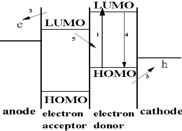
(24) electric field which drives separated charge carriers towards the respective contacts. This electric field is seldom sufficient to break up the photo generated exciton. Instead the exciton diffuses within the organic layer until it reaches a contact, where it may be broken up supply separate charges, or recombine. Since exciton diffusion lengths are short, typically 1-10 nm, exciton diffusion limits charge carrier generation in such a device. Photo carrier generation is therefore a function not only of bulk optical absorption, but also of available mechanisms for exciton dissociation. Other loss factors are non-radiative recombination at the interfaces and non-geminate recombination at impurities or trapped charges. Single layer solar cells of this type typically deliver quantum efficiencies (QE) of less than 1 % and power conversion efficiencies of less than 0.1 %. QE is the ratio of electrons delivered to the external circuit per incident photon of a given wavelength, and is the figure of merit in organic photo voltaics. High QE is a necessary, through not sufficient, condition for high photovoltaic efficiency. In organic devices the value is still far from the values of 80-90 % typically in inorganic solar cell.. 2-4-2 Heterojunction Most of the developments that have improved performance of organic photovoltaic devices are based on donor-acceptor heterojunctions. At the interface between two different materials, electrostatic forces result from the differences in electron affinity and isolation potential. If both electron affinity and ionization potential are greater in one materials than the other then the interfacial electric field drives charge separation (Figure 2.7). These local electric fields are strong and may break up photo generated excitions provided that the differences in potential energy are larger than the exciton binding energy. In a planar heterojunction, or “bi-layer” device, the organic donor-acceptor interface. 15.
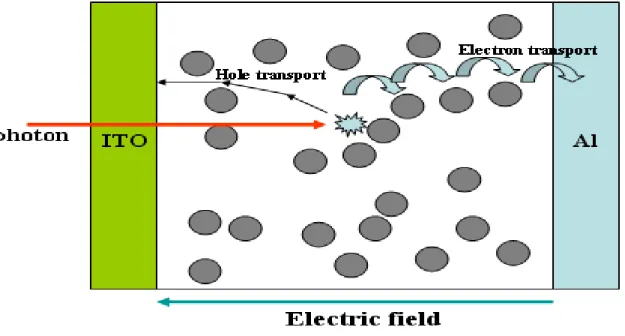
(25) separates excitons much more efficiently than the organic-metal interfaces in a single layer device and with very high purity materials, photovoltaic devices with high QE may be made.. 2-4-3 Dispersed Heterojunctions A revolutionary development in organic photovoltaic came in the mid 1990s with the introduction of a dispersed heterojunction, where an electron accepting and an electron donating materials are blended together. If the domain size in either material is similar to the exciton diffusion length, then wherever an exciton is photogenerated in that material, it is likely to diffuse to an interface and break up. If continuous paths exist in each material from the interface to the respective electrodes, then the separated charge carriers may travel to the contacts and deliver current to the external circuit (Figure 2.8). This effect was reported independently by several groups [33-35] for a blend of two conjugated polymer. The blend improved QE t around 6-8 % from less than 1 % for either polymer alone. Around the same time, Yu and co-workers reported a QE of 29 % for a blend of the hole transporter, poly-phenylene vinylene (PPV) with a derivative of C60 [36], where the C60 acts as the electron transporting component (Figure 3(b)). This was followed by observation of enhanced QE in heterojunctions made from conjugated polymers with inorganic nanocrystals [37-38] and organic dye crystals [39]. The demonstration of improved QE with dispersed heterojunction represents a departure from the device physics of conventional solar cells and has led to new device and materials designs. The principles of operation are shared by dye sensitized solar cells which are discussed in reference [40].. 16.
(26) 2-5 Organic solar cells materials Organic electronic materials are conjugated solids where both optical absorption and charge transport are dominated by partly delocalized π and π* orbits. Candidates for photovoltaic applications include crystalline or polycrystalline films of small molecules, amorphous films of small molecules prepared by vacuum deposition or solution, and combinations of any of these either with order organic solids or with inorganic materials. A comprehensive discussion of the development of organic solids for photovoltaic applications is given by Hall [41]. Organic photovoltaic materials differ from inorganic semiconductors in the following important respects [42]. 1. Photo generated excitons are strongly bound and do not spontaneously dissociate pairs of energy of ~100 meV compared to a few meV for a crystalline semiconductor. This means that charge carrier separation generation dose not necessarily result from the absorption of light. 2. Charge transport proceeds by hopping between localized states, rather than transport within a band, which results in low mobilities. 3. The spectral range of optical absorption is relatively narrow compared to the solar spectrum. 4. Absorption coefficients are high (~105 cm-1) so that high optical densities can be achieved, at peak wavelength, with films less than 100 nm thick. 5. Many organic materials are susceptible to degradation in the presence of oxygen or water. 6. As one-dimensional semiconductors, their electronic and optical properties can be highly anisotropic. This is potentially useful for devices design. The first two features are due to the fact that the intermolecular van der Waals forces. 17.
(27) in organic solids are weak compared to bonds in inorganic crystals and much weaker than the intramolecular bonds. As a consequence all electronic states are localized on single molecules and do not from bonds. Low mobility is aggravated by the high degree of disorder present in many organic solids. The optical excitations accessible to visible photons are usually π to π* transitions. Most conjugated solids absorb in the blue or green, absorption in the red or infrared is harder to achieve. However, the absorption bandwidth depends on the degree of conjugation and wider spectral sensitivity can be achieved in highly conjugated dye molecules. These properties impose some constraints on organic photovoltaic devices: 1. A strong driving force should be present to break up the photo generated excitons. 2. Low charge carrier mobilities limit the useful thickness of devices. 3. Limited light absorption across the solar spectrum limits the photocurrent. 4. Very thin devices mean interference effects can be important. 5. Photocurrent may be sensitive to temperature through hopping transport and thermal dissociation of excitons.. 18.
(28) 第三章 實驗步驟 ITO基板的處理包含以下步驟: 1. 使用丙酮清洗5分鐘,去除ITO表面的雜質污染。 2. 使用甲醇清洗5分鐘,去除ITO表面的殘留丙酮。 3. 使用去離子水在超音波振盪器中清洗10分鐘。 4. 使用氮氣吹乾ITO基板。 5. 利用旋轉塗佈法的方式在ITO表面塗上正光阻型的光阻。 6. 在烘箱中軟烤10分鐘。 7. 將ITO基板曝光,定義所需要的電極形狀。 8. 在烘箱中硬烤10分鐘。 9. 利用鹽酸蝕刻出所需要的圖案。 10. 重覆上述1~3步驟。 熱蒸鍍包含以下步驟: 1. 在蒸鍍腔體放入處理過的ITO基板,抽真空至10-6 Torr。 2. 控制材料加熱溫度及鍍率,依序鍍上所需薄膜厚度。 3. 破真空,準備量測。. 19.
(29) 元件的量測: 1. 在太陽能模擬器中,放入AM 1.5的濾鏡並且調整模擬器和元件的高度,使得照光 強度為1 SUN。 2. 利用Labview控制畫面和Keithley 2400在大氣下量測得到有機太陽能電池的電壓 和電流的關係。. 20.
(30) Chapter 3 Experiment procedure 3-1 The etching and cleaning of ITO substrate After clearing the ITO substrate, we spin coating the positive liquid photo resist on ITO glass substrate and use shadow mask by UV-ray light. Then the ITO glass substrate etches with hydrochloric acid (HCl) for 2 minutes. After etching, the ITO glass substrate puts into acetone solution for 5 minutes to remove the photo resist. Then we put the ITO glass substrate into the Methanol solution for 5 minutes to remove the acetone solution. At last, we put the ITO glass substrate into DI water ultrasonic vibration bath n for 10 minutes and dry the ITO glass substrates with N2.. 3-2 The etching and cleaning of ITO substrate In our experiments, the molecule structure of organic materials show in Figure 3.1. the CuPc is used as active layer and p-type semiconductor; C60 is used as active layer and n-type semiconductor; PEDOT:PSS is used as anode buffer layer; BPhen is used as cathode buffr layer.. 3-3 Deposition of organic thin films and electrode The schematic organic solar cells manufacture machine show in Figure 3.2. The basic device structure was fabricated as follows: ITO/CuPc/CuPc:C60/C60/BPhen/Ag. All the organic layer was deposited by thermal evaporation onto the ITO coated glass substrate in a vacuum chamber(<1*10-6 Torr). The deposition rate and thicknesses of evaporated layers were monitored by an oscillating quartz thickness monitor. The deposition rates were about. 21.
(31) 0.4Å/s for organic layer and 3Å/s for Ag. The Ag as a cathode was deposited to a thickness of 100 nm by thermal evaporation through a shadow mask, giving an active area of 0.06 cm2.. 3-4 Deposition of organic thin films and electrode Three solvents were sorbitol (98%), glycerol (99.8%) and DMSO (99.9%). The solvent was added to the PEDOT: PSS directly, and then the doped PEDOT: PSS was stirred for 30 min at room temperature. The doped PEDOT: PSS layer was formed by a spin-coating method. The spin-coatings were performed at a rotation rate of 3500 rpm for 20 sec. The doped PEDOT: PSS film was heated at 150 ℃ for 20 min on a hotplate in ambient lab conditions.. 3-5 Measurements The power conversion efficiency (PCE) was calculated from the measurement under illumination by the Oriel solar simulator producing a power intensity of 100mW/cm2 (1 SUN). The intensity of irradiation was measured by an optical power meter. The current-voltage (I-V) characteristics were measured by a Keithley 2400 programmable voltage-current source. Further evaluation by Atomic Force Microscope (AFM) was performed to analyze the roughness of surface, and by spectrophotometer (Hitachi U-3010, Japan) to study the absorptivity. All measurements of organic solar cells and organic materials were carried out in air without encapsulation.. 22.
(32) 第四章 結果與討論 學 生 使 用 的 結 構 為 ITO/CuPc(10nm)/CuPc:C60(20nm)/C60(20nm)/BPhen(5nm) /Ag,此結構為實驗室有機太陽能電池的最佳結構。CuPc 和 C60 當作本實驗的主動層 材料,最主要是因為此兩種材料在可見光波段中,具有最佳的光子吸收能力。在此基 本結構下,學生在 ITO 陽極及主動層材料 CuPc 間加入陽極緩衝層 PEDOT: PSS,並 利用摻雜效應改善 PEDOT: PSS 層的特性,先後嘗試了三種溶劑摻雜至陽極緩衝層, 分別是 sorbitol,glycerol 及 DMSO,更利用儀器分析各種溶劑摻雜至陽極緩衝層的片 電阻值,表面粗糙度及薄膜穿透度性質,最徍化後得到的元件結構為 ITO/3wt% sorbitol-doped PEDOT:PSS/CuPc(10nm)/CuPc:C60(20nm)/C60(20nm)/BPhen(5nm)/Ag 。 藉由摻雜效應能大幅提升元件效率的原因為;(1) 摻雜溶劑後的 PEDOT:PSS 導電薄 膜導電度大幅提升 (2) PEDOT:PSS 導電膜使得 ITO 陽極與主動層材料 CuPc 獲得更 好的接觸 (3) 加入陽極緩衝層 PEDOT:PSS 使得載子的導出更有效率,因此,加入陽 極緩衝層 3wt% sorbitol-doped PEDOT:PSS 後的元件效率從 1.28%提升至 3.37%。 為了更進一步改善元件的載子收集效率,學生利用摻雜效應改善陰極緩衝層, 元 件 結 構 為 ITO/3wt% sorbitol-doped PEDOT:PSS/CuPc(10nm)/CuPc:C60(20nm) /C60(20nm)/Cs2CO3:BPhen(5nm)/Ag,在陰極緩衝層 BPhen 加入碳酸銫,能夠降低 C60/Cs2CO3:BPhen 之間的電子傳輸能障,故能加強電子傳輸之效率,進而增加短路電 流,此外,藉由碳酸銫的添加能夠改善陰極緩衝層的表面粗糙度,使得陰極緩衝層能 跟電極有更好的接觸。在摻雜比例 Cs2CO3:BPhen (1:4)時,元件效率提昇至 3.51%。. 23.
(33) Chapter 4 Result and Discussion In our experiment, the structure of organic solar cell (OSC) is shown in Fig. 4.1. And the schematic energy levels of the device is shown in Fig. 4.2. The performance of different structured organic solar cells was investigated. The electrical characterization, morphology and optical quality on photovoltaic devices with different solvent-doped PEDOT: PSS layers were discussed. The addition of solvent results in the obviously improvement in JSC and FF. The result shows that the device with solvent-doped PEDOT:PSS layer can exhibit higher efficiency. And the device with 3wt% sorbitol-doped PEDOT:PSS layer exhibits the highest efficiency. In addition, the thin layer of cesium carbonate-doped BPhen (Cs2CO3: BPhen) is adopted as the buffer layer of the cathode. The parameters of the cell depended on the doping concentration of the Cs2CO3: BPhen layer. The cell with Cs2CO3: BPhen (1:4) layers exhibits PCE of 3.51% as compared to 3.37% for the device with pristine BPhen layer. The improved PCE in cell was considered as favorable energy level alignment between Cs2 CO3: BPhen layer and the C60 layer. In addition, the surface morphology is improved by adding Cs2CO3 to BPhen layer.. 4-1 The insertion of the solvent-doped PEDOT:PSS layer as the anode buffer layer The performance parameters of devices with various solvent concentrations and the pristine PEDOT: PSS layer were listed in Table 4.1. These solvent-doped PEDOT: PSS are sorbitol-doped PEDOT: PSS (referred here as S-PEDOT: PSS), glycerol-doped PEDOT: PSS (referred here as G-PEDOT: PSS) and DMSO-doped PEDOT: PSS (referred here as D-PEDOT: PSS). In Table 4.1, the PCE of device is extremely low by inserting the pristine 24.
(34) PEDOT: PSS layer. On the other hand, the PCE of devices with different solvent-doped PEDOT: PSS layers are dramatically improved. The series resistance (RS) of device with pristine PEDOT: PSS layer is one hundred times higher than that of solvent-doped PEDOT: PSS layers. The difference of PCE is due to the reason that RS is substantially reduced, resulting in a sharp increase in JSC and fill factor (FF). It was found that the sheet resistance (R□) of PEDOT: PSS layer can be decreased by the addition of solvents [43]. Reduced R□ makes the holes transport more efficient. However, the key point for a decrease in RS may be attributed to the low R□ of doped PEDOT: PSS layer for all devices with the same structure.. 4-2 The sheet resistance and morphology of solvent-doped PEDOT:PSS layer Figure 4.3 shows the R□ and surface roughness (Rrms) of the various doped PEDOT: PSS films. By adding solvent, R□ and surface roughness of the films were changed with the solvent concentration. In other words, the R□ of the film decreases with increasing solvent concentration in the PEDOT: PSS. And the surface roughness increases with increasing solvent concentration. This is due to the fact that the amount of the PEDOT to PSS molar ratio at the surface is increased [43, 44], and that more PEDOT, which is a conductive material, will be clustered at the surface of the PEDOT: PSS film after doping solvent. However, this clustered phenomenon results in a decrease in R□ and an increase in roughness of surface. The reduced R □ was able to enhance carriers transport to electrode. And then the increased surface roughness may make the carriers to be trapped in defects. That is to say, we have to strike a balance between the R □ and surface morphology to obtain optimal performance. The optimal solvent concentration is 3 wt% S-PEDOT: PSS because of its lowest R□ and good morphology quality. In Table 4.2, the. 25.
(35) conductivity of the S-PEDOT: PSS was present. And the PCE of OSC with 3 wt% S-PEDOT: PSS is up to 3.37% which is higher than that of other devices with different solvent concentrations. The R □ and surface roughness of PEDOT: PSS layer were considered the main factors, which influenced the device performance.. 4-3 The transmittance of various doped anode buffer layers Figure 4.4 shows the transmittance of the PEDOT: PSS films doped with different optimal solvent concentrations on the ITO-glass substrate. Three optimal doped PEDOT: PSS are 3 wt% S-PEDOT: PSS, 4 wt% G-PEDOT: PSS and 15 wt% D-PEDOT: PSS, respectively. Among these, the optical quality in the visible region for the film of 3 wt% S-PEDOT: PSS is superior to other doped films. The transmittance spectra of 3 wt% S-PEDOT: PSS was different from spectra of 4 wt% G-PEDOT: PSS and 15 wt% D-PEDOT: PSS which is higher transmittance from 400nm to 700nm. The superior transmittance will be beneficial to absorb more photons that may obtain higher JSC. The PCE of the device with 3 wt% S-PEDOT: PSS layer is higher than that of other devices because of its better transmittance in the visible region. However, the performance of doped PEDOT: PSS devices was influenced by transmittance besides R□ and surface roughness of film.. 4-4 The EQE spectrum of the devices with various doped anode buffer layers To further verify the optical quality of the doped PEDOT: PSS films, we used QE measurement system to measure the EQE spectra of the devices. Fig. 4.5 shows the EQE of the devices with different optimal solvent-doped PEDOT: PSS layer. The EQE is 26.
(36) defined as the ratio of the number of charge carriers collected by the solar cell to the number of photons of a given energy shining on the solar cell. The EQE value is related to JSC of the device. It is found that the spectra of EQE were similar to the transmittance spectra. The device with 3wt% S-PEDOT: PSS layer has higher EQE value from 400 nm to 700 nm in the visible region. The increase EQE value is attributed to the superior transmittance of 3wt% S-PEDOT: PSS film, which makes the device absorb more photons. All the above results show that the JSC and FF depend on the quality of the device with solvent doped PEDOT: PSS film. The photons which illuminated the active area of OSC were efficiently converted into charges in the device with 3 wt% S-PEDOT: PSS layer because of its good enough quality in R□, surface roughness and transmittance. Thus, the cell with 3 wt% S-PEDOT: PSS layer could reveal the best performance.. 4-5 The improvement of cathode buffer layer by addition of Cs2CO3 The cells are fabricated in this structure ITO/ PEDOT: PSS/ CuPc/ CuPc: C60/ C60/ BPhen/ Ag, as shown in Fig. 4.6(a). The thickness of this structure was optimized by our group. And the schematic energy level of the device is shown in Fig. 4.6(b). Figure 4.7 plots the J-V characteristics of devices incorporating a 5 nm Cs2CO3: BPhen layer with various ratios and the J-V property of device with a 5 nm pristine BPhen layer. In Fig. 4.7, the device with Cs2CO3: BPhen (1:4) layer shows the superior JSC compared to other devices, implying that the Cs2CO3: BPhen (1:4) layer provide the optimal property of carriers transportation [45]. As shown in Fig. 4.8, the Cs2CO3 doping in BPhen layer causes a shift of the UPS spectra, which towards higher binding energy. It indicates the Fermi level movement in the energy gap towards the lowest unoccupied molecular orbital. 27.
(37) (LUMO). The Cs2CO3 doping causes the downward shift of the highest occupied molecular orbital (HOMO) and LUMO in BPhen layer, leading to increase in electron concentration in Cs2CO3: BPhen layer and reduction in barrier height of electron extraction. Therefore, electron extraction at the interface of C60/ Cs2CO3: BPhen is enhanced, resulting in obvious increase of JSC. In addition, the Cs2CO3: BPhen layer can be adopted as a hole blocking layer to prevent holes to the cathode, which reduces the probability of the carrier recombination. Therefore, the optimal ratio of Cs2CO3: BPhen layer is 1:4. And the PCE of OSC with Cs2CO3: BPhen (1:4) layer is up to 3.51%, which is higher than that of other devices with different ratios of Cs2CO3: BPhen layer.. 4-6 The characteristics of devices incorporating Cs2CO3:BPhen layer with different ratios and the device with pristine BPhen layer These performance parameters of devices incorporating Cs2CO3: BPhen layer with different ratios and the device with pristine BPhen layer were listed in Table 4.3. From Table 4.3, it can be seen that the VOC of the four devices are not significantly changed with different Cs2CO3 concentrations. The device with Cs2CO3: BPhen (1:4) layer shows the enhanced PCE compared to device with the pristine BPhen layer. On the other hand, the devices with other ratios of Cs2CO3: BPhen layer showed the poor PCE. In Table 1, the device with the Cs2CO3: BPhen (1:4) layer contains the lowest series resistance (RS) and the highest JSC. The Cs2CO3 doping with suitable ratio can assist the efficiency of carrier transportation, which leads to an increase in JSC and a decrease in RS. In contrast, the phenomenon in high proportion of Cs2CO3 doping is not good for JSC and RS. In particular, the device with the Cs2CO3: BPhen (4:4) layer shows the poor FF because of its huge RS.. 28.
(38) It implies that Cs2CO3 contains very low conductivity, which leads to the poor transportation of carrier to cathode. Therefore, the Cs2CO3: BPhen layer with the high Cs2CO3 concentration causes the low PCE of the device. However, the Cs2CO3 doping results in favorable energy level alignment and a decrease in carrier mobility. It is necessary to balance the energy level alignment and the Cs2CO3 concentration to obtain optimal performance. Thus, the device with the Cs2CO3: BPhen (1:4) layer shows the best performance.. 4-7 The analysis of the morphology and optics of the devices incorporating Cs2CO3:BPhen layer with different ratios and the device with pristine BPhen layer To understand that the morphology of the cathode buffer layer was related to device performance, the surface roughness of the cathode buffer layer is evaluated by AFM. Figure 4.9 shows the root mean square roughness (Rrms) of the pristine BPhen film and Cs2CO3: BPhen layer with the ratio 1:4, 2:4 and 4:4. And the Rrms value are 8.969, 6.606, 6.446, 6.039 nm, respectively. In pristine BPhen layer, the Rrms value was apparently higher than the value of the Cs2CO3: BPhen layer. This indicates that the Cs2CO3 doping is benefit to the morphology of the cathode buffer layer. The cathode buffer layer could be filled with Cs2CO3 to smooth roughness. The Rrms of Cs2CO3: BPhen layer with various ratios are almost the same. Whichever concentration of the Cs2CO3 doping is used, the morphology of BPhen layer will be improved. The morphology of the cathode buffer layer becomes smoother by Cs2CO3 doping that seems to fill the depressions. The good morphology of the cathode buffer layer causes the good contact with the cathode which avoids the carriers trapping in defects. Thus, the Cs2CO3 doping provides not only. 29.
(39) favorable energy level alignment but also smooth morphology of the cathode buffer layer. To clarify the property of the doped cathode buffer layer, the absorption of pristine BPhen and Cs2CO3: BPhen (1:4) layer was measured. In Fig. 4.10, the absorption spectra of Cs2CO3: BPhen layer was similar to BPhen layer’s. This indicates that the Cs2CO3 doped into the BPhen layer without additional absorption. That is to say, the improvement in JSC is due to changes of efficiency in carrier transportation rather than chemical changes. Thus, the enhanced performance of the device with Cs2CO3: BPhen (1:4) layer was not attributed to absorption increase. It was attributed to favorable energy level alignment and smooth morphology. To further verify that the Cs2CO3 doping into BPhen layer enhances the efficiency of the device, we used quantum efficiency (QE) measurement system to measure the EQE spectrum of the devices with pristine BPhen layer and Cs2CO3: BPhen (1:4) layer. The EQE is defined as the ratio of the number of charge carriers collected by the solar cell to the number of photons of a given energy shining on the solar cell. In Fig. 4.11, the device with Cs2CO3: BPhen (1:4) layer has higher EQE value from 350 nm to 800 nm. The enhanced EQE value is due to the increase of the charge carriers collected by electrodes, which is benefit to enhancement of JSC. The most important cause of the increased EQE value is favorable energy level alignment, which leads to the efficient transportation of the electrons to cathode. This enhanced EQE value corresponds with the enhanced JSC of the device. Thus, the EQE value verifies that the Cs2CO3 doping is good for conversion efficiency of photons into charge carriers.. 30.
(40) 第五章 結論與未來工作 以實驗室最佳化的結構作改善,以 PEDOT:PSS 導電液作為陽極緩衝層,效果不 如預期,於是摻雜溶劑於 PEDOT:PSS 導電液中,實驗結果發現元件加入摻雜的陽極 緩衝層,其效率大幅提升,最主要的原因為摻雜後的 PEDOT:PSS 導電率大幅提升, 使得元件電洞傳輸至陽極的效率大幅提升,元件的短路電流獲得大幅度的改善從原本 未加入陽極緩衝層的 5.13 mA/cm2,大幅增加至 15.45 mA/cm2,在三種溶劑山梨醣醇、 甘油及 DMSO 中,PEDOT:PSS 導電液摻雜 3wt%的山梨醣醇有最好的表現,在導電 度、薄膜平整度、穿透率方面都有很好的表現,使得摻雜山梨醣醇的 PEDOT:PSS 導 電膜能穿透得最多的光子,並且有效率地將電洞導引至電極。元件效率從 1.28%上升 至 3.37%。 接下來,學生試圖改善陰極緩衝層的特性,利用碳酸銫摻雜至陰極緩衝層 BPhen 中,摻雜碳酸銫使得 BPhen 層的能階變化,能夠同時降低 HOMO 及 LUMO,使得電 子導出至陰極時的能障減少,此外,摻雜碳酸銫能夠改善原本 BPhen 薄膜粗糙的特 性,使得陰極緩衝層更為平整,能夠與陰極銀有更好的接觸,減少缺陷的產生,電子 導出效率獲得提升,使得元件短路電流增加,元件效率提升為 3.51%。 在未來工作方面,我們可以嘗試其他材料作為陽極緩衝層,例如三氧化鎢,三 氧化鉬,這兩種材料作為陽極緩衝層都有不錯的表現,而且其穩定性要比 PEDOT:PSS 更好,另外,可以在製程中加入氧電漿來處理陽極 ITO,有了氧電漿的處理,能夠使 ITO 的功函數增加及 ITO 表面更為平整,這些改善將有助於有機太陽能電池元件效 率的提升。元件的面積也朝大面積上去做改進,並且在元件壽命上面去做探討,使得 有機太陽能電池在實用性方面能有所提升。. 31.
(41) Chapter 5 Conclusion and Future work 5-1 Conclusion The device with solvent-doped PEDOT: PSS shows the superior PCE of the OSC. Reduced R□ makes a sharp decrease in RS, which leads to higher JSC and FF. The improvement in R□ by adding solvent was attributed to the morphology change, i.e., a higher PEDOT to PSS molar ratio at the surface of PEDOT: PSS film. For the device with 3 wt% S-PEDOT: PSS layer, the lowest RS was obtained, resulting from the optimal balance between the R□ and the surface roughness. Furthermore, the film of S-PEDOT: PSS contains the best optical transmittance in visible region among all solvent-doped films, resulting in the highest JSC to enhance the PCE. However, the PCE of the device with 3 wt% sorbitol-doped PEDOT: PSS layer is up to 3.37%. In addition, the thin layer of cesium carbonate-doped BPhen (Cs2CO3: BPhen) is adopted as the buffer layer of the cathode. The performance of the devices with Cs2CO3:BPhen layer depends on the concentration of the Cs2CO3. The LUMO and HOMO of BPhen layer can be downward shifted by Cs2 CO3 doping. And this effect reduced the barrier height of electron extraction. The photons which illuminated the active area of OSC were efficiently converted into charges in the device with Cs2CO3:BPhen (1:4) layer because of its good enough quality in level alignment and smooth morphology. Thus, the cell with Cs2CO3:BPhen (1:4) layer could reveal the best performance. The cell with Cs2CO3: BPhen (1:4) layers exhibits PCE of 3.51% as compared to 3.37% for the device with pristine BPhen layer.. 32.
(42) 5-2 Future work In the future work, we can try the different materials as anode buffer layers, such as WO3, MoO3, etc. Those materials were reported as the anode buffer layer in organic solar cells because of its superior stability. And the method of ITO treatment can be applied. The oxygen plasma has been confirmed that it can increase the work function of ITO and smooth the morphology of ITO. The improvements could result in the enhanced performance of organic solar cells. In addition, the active area of device should be increased and the life time of the device should be research for the future applications.. 33.
(43) Reference [1] J.Y. Kim, Nelson E. Coates, D. Moses, T. Nguyen, M. Dante, K. Lee, A.J. Heeger, Science 317 (2007) 222. [2] Jenny Nelson, The Physics of solar cells, (London), 3. [3] F.C. Krebs, H. Spanggard, T. Kjær, M. Biancardo, J. Alstrup, Mater. Sci. Eng. B 138 (2007) 106. [4] F.C. Krebs, Sol. Energy Mater. Sol. Cells 93 (2009) 1968. [5] Wallace, Conjugated polymers: New materials for photovoltaic, Chemical Innovation 30 (2004) 15. [6] Brabec and Hummelen, “Plastic solar cells”, Adv. Funct. Mater 11 (2001) 15. [7] Halls and Friend, Organic Photovoltaic Devices, Clean Electricity from Photovoltaic, p. 377. [8] F. Padinger, R. S Rittberger and N. S Sariciftci, Adv. Funct. Mater. 13 (2003) 85. [9] V. D Mihailetchi, P. W. M Blom, J. C Hummelen and M. T Rispens, J. Appl. Phys. 94. (2003) 6849. [10] G. Li, V. Shrotriya, Y. Yao and Y. Yang, J. Appl. Phys. 98, (2005) 043704. [11] M.C Scharber, D.Muhlbacher, M. Koppe, P. Denk, C. Waldau, A. J. Heeger and C.J. Brabec, Adv. Mater. 18, (2006) 789. [12] L. J A. Koster and P. W. M Blom, Appl. Phys. Lett. 88, (2006) 093511. [13] Chiou-Hua Liu, Sheng-Fu Horng, Hsin-Fei Meng, Dark-Carrier Recombination in Organic Solar cells, (2008) 5. [14] C. J Brabec, A. Cravino, D. Meissner…etc, Adv. Funt. Mater. 11, (2001) 374. [15] Chiou-Hua Liu, Sheng-Fu Horng, Hsin-Fei Meng, Dark-Carrier Recombination in. 34.
(44) Organic Solar cells, (2008) 6. [16] P. Sullivan, S. Heutz, S. M. Schultes, T. S. Jones, Appl. Phys. Lett. 84 (2004). [17] P. Peumans, S. R. Forrest, Appl. Phys. Lett. 79 (2001). [18] Z. R. Hong, Z. H. Huang, X. T. Zeng, Chem. Phys. Lett. 425 (2006). [19] Vibha Tripathi, Debjit Datta, G. S. Samal, Asha Awasthi, Satyendra Kumar,Journal of non-crystalline solids 354 (2008). [20] Q. L. Song, F. Y. Li, H. Yang, H. R. Wu, X. Z. Wang, W. Zhou, J. M. Zhao, X. M. Ding, C. H. Huang, X. Y. Hou, Chem. Phys. Lett. 416 (2005). [21] Z. R. Hong, Z. H. Huang, X. T. Zeng, Thin solid films 515 (2007). [22] Thekackara, NASA Technical Report, No. R-351 (1970). [23] Thekackara, Suppl. Proc. 20th. Annu. Meet. Inst, 21, (1974). [24] Bakus, solar cell, New York: IEEE Press, (1980). [25] Henry, J. Appl. Phys., 15 (1980) 4494. [26] Terrsetial Photovoltaic Measurement Procedures, ERDA/NASA Report, 1022-77/16, (1977). [27] Hans Joachim Moller, “Semiconductor for solar cell”, pp. 9-11. [28] Jenny Nelson, The Physics of solar cells, London, p. 36. [29] Hans Joachim Moller, Semiconductor for solar cell, p. 48. [30] Tom Markvart and Luis Castaner, Solar Cells, p. 11. [31] Hans Joachim Moller, Semiconductor for solar cell, pp. 49-50. [32] Larry D. Partain, Solar cells and their applications, p. 22. [33] Yu. G. and Heeger, J. Appl. Phys. 78 (2007) 4510-4515. [34] Yoshino, IEEE Transactions on Electron Devices, ED-44 (2008), 1315-1324. [35] Halls, J. J. M., Nature, 376, 498-550. [36] Yu. G…etl., Science, 270 (1995) 1789-1791.. 35.
(45) [37] Greenham and Alivistatos, Physical Review B, 54 (24), pp.17628-17637. [38] Salfsky, Physical Review B, 59 (16), pp.10885-10894. [39] Petritsch, Solar Energy Materials and Solar Cells, 61 (2001) 63-72. [40] Hagfeldt, Accounts of Chemical Research, 33 (2005) 269-277. [41] Halls and Friend, Clean Electricity from Photovoltaic, p. 377. [42] Tom Markvart and Luis Castaner, Solar Cells, p. 420. [43] S.K.M. Jönsson, J. Birgerson, X. Crispin, G. Greczynski, W. Osikowicz, A.W. Denier van der Gon, W.R. Salaneck, M. Fahlman, Synth. Met. 139 (2003) 1-10. [44] Jingsong Huang, Paul F. Miller, Jo S. Wilson, Andrew J. de Mello, John C. de Mello, Donal D.C. Bradley, Adv. Funct. Mater. 15 (2005) 290–296. [45] Y. Cai, H. X. Wei, J. Li, Q. Y. Bao, X. Zhao, S. T. Lee, Y. Q. Li, and J. X. Tang, Appl. Phys. Lett. 98 (2011) 113304.. 36.
(46) 160 140. dollars/pail. 120 100 80 60 40 20 0 1970. 1975. 1980. 1985. 1990. 1995. 2000. year Fig. 1.1. Oil prices, 1970-2008.. 37. 2005. 2010.
(47) Fig. 2.1. Solar spectrum [47].. 38.
(48) Fig. 2.2. The equivalent circuit of a solar cell.. 39.
(49) Fig. 2.3. I-V characteristics of solar cell.. 40.
(50) Fig. 2.4. The equivalent circuit of solar cell with Rs and Rsh.. 41.
(51) Fig. 2.5. Plots of the equation for various combinations of the series and shunt resistance.. 42.
(52) (a). (c). (b). Fig. 2.6. Schematic energy-band diagram of a simple device consisting of single organic layer between two metal contacts.. 43.
(53) Fig. 2.7. Schematic of energy-band diagram of a donor-acceptor heterojunction.. 44.
(54) Fig. 2.8. A blend of two polymers [48].. 45.
(55) Fig. 2.9. A blend of one polymer with electron accepting nanoparticles or fullerene.. 46.
(56) Fig. 4.1. Schematic structure of the organic photovoltaic cells.. 47.
(57) Fig. 4.2. Schematic energy levels of the device.. 48.
(58) Fig. 4.3. Comparison of the sheet resistance and surface roughness with various (a) sorbitol-doped (b) glycerol-doped (c) DMSO-doped PEDOT: PSS concentrations on the ITO-glass substrate. 49.
(59) Fig. 4.4. The transmittance of different doped PEDOT: PSS with optimal concentration on the ITO-glass substrate.. 50.
(60) Fig. 4.5. The EQE of different doped PEDOT: PSS with optimal concentration on the ITO-glass substrate.. 51.
(61) Fig. 4.6. (a) Schematic structure of the organic photovoltaic cells and (b) schematic energy levels of the device.. 52.
(62) Fig. 4.7. J-V characteristics of the small molecule organic solar cells with different cathode buffer layers.. 53.
(63) Fig. 4.8. UPS spectra of pristine BPhen and Cs2CO3:BPhen (1:4) films.. 54.
(64) Fig. 4.9. AFM images of the (a) pristine BPhen, (b) Cs2CO3:BPhen (1:4), (c) Cs2CO3:BPhen (2:4), (d) Cs2CO3:BPhen (4:4) layer evaporated on the ITO/ PEDOT:PSS/ CuPc/ CuPc:C60/ C60.. 55.
(65) Fig. 4.10. The absorption spectra of pristine BPhen and Cs2CO3:BPhen(1:4) layer.. 56.
(66) Fig. 4.11. The EQE of the device with BPhen layer and the device with Cs2 CO3:BPhen(1:4) layer.. 57.
(67) Tab.1.1. Efficiency of solar cells.. 58.
(68) Tab.2.1. Integrated Solar Energy Received Annually in Various Countries.. 59.
(69) Table 4. 1. Photovoltaic performance parameters of different devices.. 60.
(70) Table 4. 2. The conductivity of PEDOT: PSS layers doped with different sorbitol concentrations. Conductivity (S/cm) PEDOT:PSS PEDOT:PSS(1wt% sorbitol). 0.03 0.28. PEDOT:PSS(2wt% sorbitol). 0.86. PEDOT:PSS(3wt% sorbitol). 0.92. PEDOT:PSS(4wt% sorbitol). 0.97. PEDOT:PSS(5wt% sorbitol). 0.98. 61.
(71) Table 4. 3. The current-voltage characteristics of the devices with different cathode buffer layers.. 62.
(72)
數據
![Fig. 2.1. Solar spectrum [47].](https://thumb-ap.123doks.com/thumbv2/9libinfo/8788160.218992/47.892.135.776.366.850/fig-solar-spectrum.webp)
+7
![Fig. 2.8. A blend of two polymers [48].](https://thumb-ap.123doks.com/thumbv2/9libinfo/8788160.218992/54.892.237.734.426.725/fig-a-blend-of-two-polymers.webp)
相關文件
You are given the wavelength and total energy of a light pulse and asked to find the number of photons it
Reading Task 6: Genre Structure and Language Features. • Now let’s look at how language features (e.g. sentence patterns) are connected to the structure
Promote project learning, mathematical modeling, and problem-based learning to strengthen the ability to integrate and apply knowledge and skills, and make. calculated
Wang, Solving pseudomonotone variational inequalities and pseudocon- vex optimization problems using the projection neural network, IEEE Transactions on Neural Networks 17
volume suppressed mass: (TeV) 2 /M P ∼ 10 −4 eV → mm range can be experimentally tested for any number of extra dimensions - Light U(1) gauge bosons: no derivative couplings. =>
Estimated resident population by age and sex in statistical local areas, New South Wales, June 1990 (No. Canberra, Australian Capital
(c) Draw the graph of as a function of and draw the secant lines whose slopes are the average velocities in part (a) and the tangent line whose slope is the instantaneous velocity
Consistent with the negative price of systematic volatility risk found by the option pricing studies, we see lower average raw returns, CAPM alphas, and FF-3 alphas with higher
