Transport through a quantum ring, dot, and barrier embedded in a nanowire in magnetic field
Vidar Gudmundsson,1Yu-Yu Lin,2Chi-Shung Tang,3Valeriu Moldoveanu,4Jens Hjorleifur Bardarson,1and Andrei Manolescu1,4
1Science Institute, University of Iceland, Dunhaga 3, IS-107 Reykjavik, Iceland 2Department of Electrophysics, National Chiao Tung University, Hsinchu 30010, Taiwan 3Physics Division, National Center for Theoretical Sciences, P. O. Box 2-131, Hsinchu 30013, Taiwan
4Institute of Physics and Technology of Materials, P. O. Box MG7, Bucharest-Magurele, Romania 共Received 15 December 2004; published 2 June 2005兲
We investigate the transport through a quantum ring, a dot, and a barrier embedded in a nanowire in a homogeneous perpendicular magnetic field. To be able to treat scattering potentials of finite extent in a magnetic field we use a mixed momentum-coordinate representation to obtain an integral equation for the multiband scattering matrix. For a large embedded quantum ring we are able to obtain Aharonov-Bohm type of oscillations with superimposed narrow resonances caused by interaction with quasibound states in the ring. We also employ the scattering matrix approach to calculate the conductance through a semiextended barrier or well in the wire. The numerical implementations we resort to in order to describe the cases of weak and intermediate magnetic field allow us to produce high resolution maps of the “near field” scattering wave functions, which are used to shed light on the underlying scattering processes.
DOI: 10.1103/PhysRevB.71.235302 PACS number共s兲: 78.67.⫺n, 75.75.⫹a, 72.30.⫹q
I. INTRODUCTION
The influence of a single impurity on the conductance of a quasi-one-dimensional quantum channel has been investi-gated by several groups theoretically1–4and experimentally.5 Commonly the impurities are considered to be short range and represented by a␦ function, though treatments of more extended scatterers, like square barriers,2 can be found. Re-cently, the application to nanosized systems has spurred the use of general methods built on the Lippmann-Schwinger equation or the equivalent T-matrix formalism to describe the scattering of more general extended potentials in quan-tum channels6or curved wires.7
The inclusion of a constant homogeneous magnetic field perpendicular to the quasi-one-dimensional electron channel or wire drastically changes the properties of the system. Without the magnetic field a centered symmetric scattering potential leads to “selection rules” that restrict the possible scattering processes. These are lifted by the magnetic field, resulting in a rich structure contrasted with the conductance steps in an ideal wire as long as the magnetic length is not much shorter than the width of the wire and the range of the scattering potential.8
The character of the Lorentz force does not allow us to establish a simple multimode formulation of the scattering process in configuration space,4 but in a strong magnetic field Gurvitz used a scheme to develop a multimode formal-ism using a Fourier transform with respect to the transport direction, and a truncation to a two-mode formalism allowed him to seek analytical solutions for a short range scatterer present in a wire with general confinement.9
Here we extend this formalism by noting that in the case of a parabolic shape of the wire confinement we obtain coupled Lippmann-Schwinger equations with a nonlocal scattering potential in Fourier space for the different modes. A transformation of this system of equations to correspond-ing equations for the T matrix shows that it bears a strong
resemblance to the corresponding equations for the system in no external magnetic field.6We exploit this fact to seek nu-merical solutions for the system in weak and intermediate strength of the magnetic field where a two-mode approxima-tion is not always warranted. One benefit of the numerical approach is that it allows us to map out with high resolution the probability density for the scattering states near the scat-terer. These “near field” solutions give us a good indication of the scattering process itself. We explore a quantum wire with an embedded quantum dot or a ring. We are able to increase the size of the ring to the limit where we observe Aharonov-Bohm type of oscillations.
In order to investigate the scattering of potentials that are homogeneous in the direction perpendicular to the wire rep-resenting a barrier or a well we employ an alternative faster method based on mode matching. The smooth scattering po-tential is sliced into a series of␦ potentials. The scattering matrix is then constructed from repeated mode matching at each slice. This mode matching approach is faster since the homogeneity of the scattering potential in the transverse di-rection is explicitly used in its numerical implementation, but the formalism built on the Lippmann-Schwinger approach is kept general, applicable for any reasonable localized poten-tial.
II. MODELS
We consider electron transport along a parabolically con-fined quantum wire parallel to the x axis and perpendicular to a homogeneous magnetic field B = Bzˆ. In the center of the wire the electrons are scattered by a potential Vsc共r兲 to be specified below. The system under investigation is described by the Hamiltonian H = H0+ Vsc共r兲 with
H0= ប2 2m*
冋
− i − eB បcyxˆ册
2 + Vc共y兲, 共1兲where the wire is assumed to be parabolically confined, namely, Vc共y兲=m*⍀
0
2y2/ 2 with m* and ⍀
respec-tively, the effective mass of an electron in GaAs-based ma-terial and the confinement parameter. Here −e is the charge of an electron. We present two quite different approaches to describe the scattering process of incoming electron states, one using wave function matching appropriate to describe scattering from a thin homogeneous barrier or well perpen-dicular to the wire, and the other one using a T matrix for-malism to calculate the scattering of an embedded quantum dot or ring in the wire.
A. Scattering matrix via mode matching
In this section, we employ a mode matching approach to the calculation of a coherent electronic transport in a quan-tum wire in the presence of a Gaussian-profile scattering po-tential. The potential under investigation can be realized as a finger gate atop the wire and can be modeled by
Vsc共r兲 = V0exp共−x2兲, 共2兲
as is shown in Fig. 1.
To obtain a dimensionless expression we employ the Bohr radius a0, and have thus the relevant units for the confine-ment parameter ⍀0*=ប/共m*a
0
2兲 and the magnetic field B*=បc/共ea
0
2兲. As such, by defining the unit of the cyclotron frequency to bec*=⍀0*, the cyclotron frequency simply has the dimensionless formc= B.
In the absence of scatterers the eigenfunctions of H0 can be written as9±共x,y,k
n兲=e±iknx±共y,kn兲 with ±knbeing the
wave vector along ±xˆ in the nth transverse subband, where
±共y,k
n兲 satisfies the reduced dimensionless equation
冋
− 2 y2+⍀w 2共y ⫿␣ n兲 2册
±共y,k n兲 = En ±共y,k n兲, 共3兲which is a harmonic oscillator of frequency ⍀w with a
shifted center ␣n=ckn/⍀w
2. These eigenmodes of the elec-tron in a state described by共x,y,kn兲 in a pure quantum wire
have the energy spectrum E = En+K共kn兲, composed of
Lan-dau levels En=共n+1/2兲⍀w, where⍀w=
冑
c2+⍀ 0
2, shifted by the confining potential, and the kinetic energy
K共kn兲=kn
2共⍀
0/⍀w兲2. The eigenfunctions ±共y,kn兲 of the
eigenmodes are given by
±共y,k n兲 = NnHn关
冑
⍀w共y ⫿␣n兲兴exp冋
− ⍀w 2 共y ⫿␣n兲 2册
, 共4兲 where Nn=共⍀w/兲1/4共2nn!兲−1/2 is a normalization constant.Using the scattering-matrix method and piecewise match-ing共see Appendix A兲,10,11one can obtain the transport equa-tions
兺
n⬘ Imn+ ⬘共kn⬘兲tn⬘n i −兺
n⬘ Imn− ⬘共kn⬘兲rn⬘n i = Imn+ 共kn兲 共5兲 and兺
n⬘ Jmn+ ⬘共kn⬘兲tn⬘n i +兺
n⬘ Kmn− ⬘共kn⬘兲rn⬘n i = knImn + 共k n兲, 共6兲where the matrix elements are related to the overlap integrals
Imn ⬘ ± =
冕
m共y兲n⬘ ±共y兲dy, 共7兲 Jmn ⬘ + 共k n⬘兲 = kn⬘Imn⬘ + 共k n⬘兲 + iV0Vmn⬘ + 共8兲 with Vmn ⬘ + =冕
m共y兲Vsc共y兲n ⬘ ±共y兲dy 共9兲 and Kmn ⬘ − 共k n⬘兲 = kn⬘Imn⬘ − 共k n⬘兲. 共10兲Using Eqs. 共5兲 and 共6兲 and the corresponding equations for r˜n ⬘n i and t˜n ⬘n i
, one can establish the scattering matrix for the Gaussian-shape potential.12 From the ratio of the mitted and the incident current we obtain the currents trans-mission T␣, in which␣andare, respectively, the incident and the transmitting lead. In the following, we assume that the scattering potential is located at the center of the wire and the source-drain bias is sufficiently low. Then the zero-temperature conductance can be expressed in terms of the incident electron energy E of the form
G共E兲 =2e 2 h
兺
n=0N
Tn共E兲, 共11兲
where N denotes the highest propagating mode incident from the source electrode. The current transmission coefficient
FIG. 1. 共Color online兲 Well or barrier embedded in a quantum wire with V0=共a兲 −6 meV and 共b兲 6 meV, respectively. Other
pa-rameters are B = 0 T, aw= 33.7 nm, E0=ប⍀0= 6.0 meV, and aw2= 1.897.
Tn共E兲 for an electron incident in the nth subband from the
source electrode is given by
Tn共E兲 =
兺
n⬘共n⬘⬎0兲 kn⬘ kn 兩tn⬘n RL 兩2. 共12兲The current reflection coefficient Rn共E兲 can be calculated by
a similar form to get the current conservation condition for checking the numerical accuracy.
B. Scattering matrix via Lippmann-Schwinger formalism
We consider a quantum dot or ring embedded in the wire and parametrize the scattering potential accordingly, combin-ing two Gaussian functions of different shapes
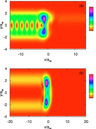
Vsc共r兲 = V1exp共−1r2兲 + V2exp共−2r2兲, 共13兲 as is shown in Fig. 2.
Together the magnetic field and the parabolic confinement define a natural length scale aw=
冑
ប/共m*兲⍀w, where
⍀w=
冑
c2
+⍀02, with the cyclotron frequency c= eB /共m*c兲,
is the natural frequency of the quantum wire in a magnetic field.
Along the lines of Gurvitz we choose to use the mixed momentum-coordinate presentation of the wave functions9
⌿E共p,y兲 =
冕
dxE共x,y兲e−ipx 共14兲and expand them in channel modes ⌿E共p,y兲 =
兺
n
n共p兲n共p,y兲, 共15兲
i.e., in terms of the eigenfunctions for the pure parabolically confined wire in a magnetic field
n共p,y兲 = exp
冋
−1 2冉
y − y0 aw冊
2册
冑
2n冑
n!aw Hn冉
y − y0 aw冊
, 共16兲 with the center coordinate y0= paw2
c/⍀w. These eigenmodes
of the pure quantum wire have the energy spectrum Enp= En+n共p兲 with En=ប⍀w共n+1/2兲 and n共p兲 = 共paw兲2 2 共ប⍀0兲2 ប⍀w . 共17兲
Using Eqs. 共14兲–共17兲 and performing a Fourier transform with respect to the coordinate x transforms the Schrödinger equation corresponding to the Hamiltonian共1兲 into a system of coupled nonlocal integral equations in momentum space,
n共q兲n共q兲 +
兺
n⬘冕
dp 2Vnn⬘共q,p兲n⬘共p兲 = 共E − En兲n共q兲, 共18兲 where Vnn⬘共q,p兲 =冕
dyn *共q,y兲V共q − p,y兲 n⬘共p,y兲 共19兲 andV共q − p,y兲 =
冕
dx e−i共q−p兲xVsc共x,y兲. 共20兲 The matrix elements共19兲 and 共20兲 for the scattering potential 共13兲 can be evaluated analytically since they consist of Gaus-sians and Hermite polynomials共see Appendix B兲.The special form of the part of the energy dispersion
n共q兲 for parabolic confinement allows us now to rewrite Eq.
共18兲 as 兵− 共qaw兲 2+关k n共E兲aw兴 2其 n共q兲 = 2ប⍀w 共ប⍀0兲2
兺
n⬘冕
dp 2Vnn⬘共q,p兲n⬘共p兲, 共21兲 where we have defined the effective band momentum kn共E兲as 共E − En兲 = 关kn共E兲兴2 2 共ប⍀0兲2 ប⍀w . 共22兲
In the absence of a magnetic field it is possible to derive an equivalent effective one-dimensional multiband Schrödinger equation equivalent to 共21兲 in coordination space.4 This multiband equation is then usually transformed into a system
FIG. 2. 共Color online兲 Quantum ring 共upper兲 or dot 共lower兲 embedded in a quantum wire, B = 0 T, aw= 33.7 nm,
E0=ប⍀0= 1.0 meV,1aw
2
= 3.41, and2aw
2
of effective one-dimensional coupled Lippmann-Schwinger integral equations that is convenient for numerical computa-tion. Here we can proceed along these lines, but the magnetic field forces us to do this in momentum space where we shall see that the corresponding Lippmann-Schwinger equations are better transformed into integral equations for the T matrix in order to facilitate numerical evaluation. Considering Eq. 共21兲 it is clear that the incoming scattering states satisfy
兵− 共qaw兲2+关kn共E兲aw兴2其n
0共q兲 = 0, 共23兲 which implies a Green’s function
兵− 共qaw兲2+关kn共E兲aw兴2其GE
n共q兲 = 1. 共24兲
The Green’s function can now be used to write down coupled Lippmann-Schwinger equations in momentum space
n共q兲 =n 0共q兲 + G E n共q兲
兺
n⬘冕
dp aw 2 V ˜ nn⬘共q,p兲n⬘共p兲, 共25兲 where V˜nn⬘共q,p兲=Vnn⬘共q,p兲2ប⍀w/关aw共ប⍀0兲2兴. These equa-tions are inconvenient for numerical evaluation as the in-staten0 is proportional to a Dirac ␦ function. Symbolically Eq.共25兲 can be expressed as=0+ GV˜, and an iteration of the equation gives =0+ GV˜0+ GV˜ GV˜0+¯ =共1 + GT˜ 兲0, where we have introduced the T matrix satisfying the symbolic equation T˜ =V˜ +V˜ GT˜. Fully written, the equa-tion determining the T matrix isT ˜ nn⬘共q,p兲 = V˜nn⬘共q,p兲 +
兺
m⬘冕
dk aw 2 V ˜ nm⬘共q,k兲GE m⬘共k兲T˜ nm⬘共k,p兲. 共26兲 This set of equations is easier to solve numerically than the equivalent Lippmann-Schwinger Eqs. 共25兲 after the singu-larities of the Green’s function have been handled with spe-cial care.13 We obtain analytically the contribution of the poles of the Green’s function and perform the remaining principal part integration by removing the singularity by sub-traction of a zero.14,15Comparison with the nonseparable two-dimensional Lippmann-Schwinger equation in configuration space for the extended scattering potential in a magnetic field gives the connection between the T matrix and the probability ampli-tude for transmission in mode n with momentum kn if the
in-state is in mode m with momentum km,
tnm共E兲 =␦nm−i
冑
共km/kn兲 2共kmaw兲冉
ប⍀0 ប⍀w冊
2 T ˜ nm共kn,km兲. 共27兲The conductance is then according to the Landauer-Büttiker formalism defined as
G共E兲 =2e 2 h Tr关t
†共E兲t共E兲兴, 共28兲 where t is evaluated at the Fermi energy.
Symbolically the wave function can be expressed as
=共1+GT˜兲0if the in-state0 is given. Together with Eqs. 共14兲 and 共15兲 this gives
E共x,y兲 = eiknxn共kn,y兲 +
兺
m冕
dq aw 2 e iqxG E m共q兲T˜ mn共q,kn兲m共q,y兲 共29兲 for an incident electron with energy E in mode n with mo-mentum kn. To calculate the wave function the same methodsare used to isolate the contribution from the poles of the Green’s function as were used for the calculation of T˜ with Eq.共26兲.
III. RESULTS A. Embedded barrier
In this section, we present our numerical results of explor-ing electronic transport properties usexplor-ing a Gaussian-shape potential model described by Eq.共2兲—the conductance ver-sus the incident electron energy E. The parameters used to obtain our numerical results are taken from the GaAs-AlxGa1−xAs heterostructure system. The values that we choose for our material parameters are ERyd= 5.93 meV and a0= 9.79 nm.
The conductance Eq.共11兲 of the wire is presented in Fig. 3 for several values of magnetic field. To explore the trans-port properties it is convenient to show the conductance as a function of energy of the incoming electron state scaled by the subband energy level spacing X = E /ប⍀w+ 1 / 2 such that
the integral values of X indicate the number of incident modes. In Fig. 3, we present the conductance for magnetic fields with strengths from 0 to 2.4 T for either weak 共V0= −6 meV兲 or strong 共V0= −12meV兲 attractive potentials, as shown in Figs. 3共a兲 and 3共b兲, respectively. For the case of the weak attractive potential shown in Fig. 3共a兲, one can see that the dip structures in G共E兲 are pinned at around X⯝n+0.85, and the location is insensitive to the magnetic field. It turns out that these structures correspond to the elec-trons incident from subband n scattered elastically into the n + 1 subband threshold forming quasibound states.6It can be demonstrated that these quasibound states are formed in the leads out of the embedded Gaussian potential.16
For the case of the strong attractive potential shown in Fig. 3共b兲, one can see that there are two types of quasibound state features. The mechanism of sharp dips below the sub-band threshold is similar to the case of the weak attractive potential. On the other hand, it is interesting to see the valley structures in Fig. 3 for B⫽0. These valleys correspond to quasibound states formed in the attractive Gaussian poten-tial. When the applied magnetic field becomes stronger, the blueshift of these valleys indicates that such quasibound states are formed closer to the edge of the Gaussian potential due to the cyclotron motion. The large width of these valley structures implies the short lifetime of these quasibound states. When increasing the strength of the magnetic field, these valleys become wider. This indicates that the electrons
in high magnetic field with short cyclotron radius easily es-cape from the quasibound states formed in such a strong attractive potential. We note in passing that in the absence of magnetic field, the intersubband transition is forbidden since the attractive potential is uniform in the transverse direction, and we cannot see any dip structures in G共E兲.
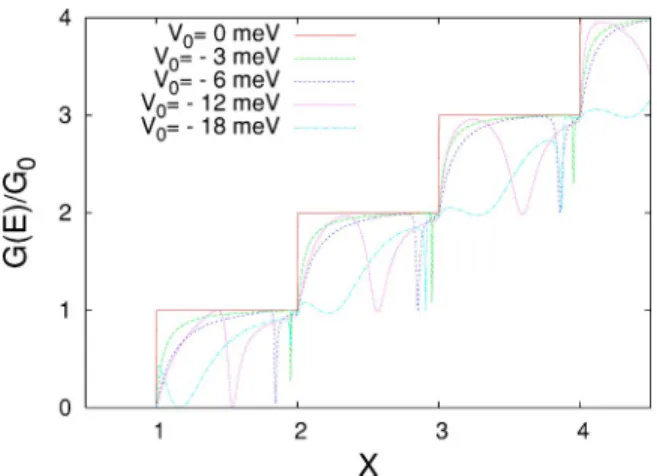
In Fig. 4, we study how the conductance can be affected by changing the amplitude of the attractive potential by fixing the strength of the magnetic field B = 1 T, the con-fining potential បy= 6 meV, and the Gaussian parameter
2aw
2共B=0兲=1.897. In the absence of the Gaussian potential 关solid 共red兲 curve兴, the electron transport manifests an ideal quantized conductance, the magnetic field plays no role. When increasing the amplitude of the attractive potential, the subband levels in the potential will decrease in energy. Therefore, we can find a redshift of the quasibound states. More precisely, for the cases of V0= −3, −6, −12, and −18 meV, the dip structures occur at around E /ប⍀w= 1.95,
1.84, 1.54, and 1.17, respectively, in the attractive potential. It is also interesting to note that when the attractive potential is very strong, such as V0= −18 meV, one can see a second dip structure appearing below the subband thresholds; both are quasibound states of the attractive potential.
Figure 5 shows the conductance as a function of incident electron energy for several values of magnetic field in the
presence of a repulsive potential. The magnetic fields are tuned from 0 to 2.4 T for either weak共V0= 6 meV兲 or strong 共V0= 12 meV兲 repulsive potentials, as shown in Figs. 5共a兲 and 5共b兲, respectively. For the case of the weak repulsive potential shown in Fig. 5共a兲, one can see that the
conduc-FIG. 3.共Color online兲 Conductance of a parabolically confined wire as a function of the energy parameter X = E /ប⍀w+ 1 / 2 for
various applied perpendicular magnetic fields. The amplitudes of the attractive impurity potential are共a兲 −6 and 共b兲 −12 meV. Other parameters areប0= 6 meV and2aw2共B=0兲=1.897.
FIG. 4.共Color online兲 Conductance of a parabolically confined wire as a function of incident electron energy for various ampli-tudes of attractive potential. The other parameters are taken to be
B = 1 T,ប0= 6 meV, and2aw2共B=0兲=1.897.
FIG. 5. 共Color online兲 Conductance as a function of incident electron energy with various applied magnetic fields. The amplitudes of the repulsive potential barrier are V0=共a兲 6 and 共b兲 12 meV. Other parameters are ប0= 6 meV. and 2aw
tance plateaus are suppressed from the ideal case. When in-creasing the applied perpendicular magnetic field, the sup-pressed conductance plateaus tend to be enhanced back to the ideal case. For the case of a strong repulsive potential 关see Fig. 5共b兲兴, the conductance curves are suppressed much more than those for the weak repulsive potential. In the ab-sence of magnetic field, the conductance increases linearly with X; while increasing the external magnetic field, the quantization behavior in G becomes slowly recognizable.
To conclude this section, we note in passing that when the scattering potential共well or barrier兲 is uniform in the trans-verse direction it does not break the translational invariance along the lateral confining direction. However, in the pres-ence of a magnetic field, if such a scattering potential is a well then one can find quasibound states due to elastic inter-subband transitions to a higher inter-subband threshold. However, if the scattering potential is a barrier, one finds no quasi-bound state features even in a magnetic field up to 2.4 T.
B. Embedded quantum ring and dot
To model an embedded quantum ring with the parametri-zation共13兲 we initially choose the parameters used in Fig. 2, such that when B = 0 then 1aw
2= 3.41,  2aw
2= 11.37, and ប⍀w= 1.0 meV.关The parameters of the potential 共13兲,1and
2 do not depend on B, but aw does.兴 V1= −12 meV and V2= 18 meV. We are thus investigating a relatively broad wire with a small embedded ring structure with diameter of approximately 40 nm. We assume the wire to be a GaAs wire as mentioned above. The conductance 共28兲 of the wire is presented in Fig. 6 for several values of the magnetic field. To compare the results for various values of the magnetic field it is convenient to observe the conductance as a func-tion of the energy of the incoming electron state scaled by the distance of the energy subbands, i.e., E /共ប⍀w兲=E/Ew, and furthermore use X = E /ប⍀w+ 1 / 2 such that the integral value of X indicates the number of incident modes.
In Fig. 6共a兲 we see that as soon as the magnetic field is different from zero a strong Fano-like17,18resonance dip ap-pears in the first plateau just above X = 1.5. As we argue below the dip corresponds to a destructive quantum interfer-ence between a quasibound state in the ring and an in-state of the wire. Figure 7 displays the total probability to find an electron in the wire close to the scattering center, the quan-tum ring. The probability is calculated using the wave func-tion共29兲 for two values of the energy of the incoming elec-tron in the lowest transverse mode, n = 0. Just below the resonance at X = 1.4, Fig. 7共a兲 reveals to us a normal scatter-ing process. The scatterscatter-ing only takes place very close to x⬇0 and on the left-hand side we see the interference pat-tern for the incoming and the reflected waves. On the right-hand side the electrons only travel in one transverse mode and only to the right so we have a constant probability al-ready a short distance away from the scattering center. The situation is quite different in Fig. 7共b兲 which displays the probability density for the state exactly in the resonance dip. Here no transmitted wave is present, but the probability close to the quantum ring is high enough that the probability for the incoming and the reflected waves is not visible on the color scale used.
The symmetry of the quasibound state indicates that it is an evanescent state belonging to the second subband n = 1. Without a magnetic field the scattering via the evanescent state in the second subband is forbidden in the case of a symmetric potential placed in the middle of the wire. In that case a dip occurs in the second band due to a scattering through a evanescent state in the third subband.2,6,19
FIG. 6.共Color online兲 The conductance of a parabolic wire with an embedded ring in units of G0= 2e2/ h. Ew=ប⍀w, V1= −12 meV, V2= 18 meV, ប⍀0= 1.0 meV, 1aw2共B=0兲=3.412, 2aw2共B=0兲
In order to further support our view that the resonance is due to a quasibound state of the quantum ring located in the continuum of the first subband共the ring lowers a state in the second subband into the first one兲, we see in Fig. 8共a兲 how the broadening or narrowing of the wire has little effect on the energy of the state. On the other hand, as seen in Fig. 8共b兲 the energy of the quasibound state changes linearly with the depth of the ring potential. The Fano resonance is formed when the in-wave is perturbed by the scattering potential and since multiple scattering is inherent in the Lippmann-Schwinger equation an attractive scattering potential can lead to resonances that are remnants of the resonances of the po-tential well in the energy continuum of the wire system.
For some intermediate values of the magnetic field we see other minima occurring in the conductance closer to the end of the first step. For example, for B = 0.8 T this is visible in Fig. 6共b兲 at X=1.933 and 1.991. The corresponding probabil-ity densities are seen in Fig. 9.
The symmetry of both densities indicates that the dips are caused by scattering via evanescent states of the second sub-band just like the dip in the middle of the first conductance step. These states are quasibound states of the ring further in the continuum of the first subband. The higher state, Fig. 9共b兲, has acquired more of the character of the geometry of the wire than the ring, and it extends far beyond the ring. The presence of Fano line shapes in the conductance is not sur-prising as the mesoscopic Fano effect was already
experi-mentally reported for both a single electron transistor20 and an Aharonov-Bohm interferometer with an embedded quan-tum dot.21,22Nevertheless, in these two experiments the wire was much smaller than the mesoscopic system that caused the Fano interference. The results presented here suggest that this may be observed also in the case of a broad wire.
At still higher magnetic field关see Fig. 6共c兲兴, the conduc-tance has approached the ideal case as the magnetic field has now squeezed the wave functions together and closer to the edge as soon as the momentum is different from zero. The wave function thus bypasses the scattering potential. We shall see this effect clearer below.
The conductance of a wire with an embedded dot is pre-sented in Fig. 10.
The effects of an increasing magnetic field become very clear if we compare the probability density for the dip at X = 1.679 when B = 0.6 T, and the one at X = 1.557 when B = 1.2 T共see Fig. 11兲. Both cases show a partial blocking of the channel due to backscattering caused by a quasibound state created by an evanescent state of the second subband, but the main difference is the total separation of the incom-ing and the reflected channel at the higher magnetic field. At
FIG. 7.共Color online兲 The probability density of the scattering stateE共x,y兲 in the parabolic quantum wire in the presence of an
embedded quantum ring共Fig. 2兲, corresponding to the conductance in Fig. 6共a兲 at B=0.1 T. The incident energy X=1.4 共a兲 and 1.538
共b兲, corresponding to the dip in the conductance. FIG. 8.共Color online兲 The conductance of a parabolic wire with an embedded ring in units of G0= 2e2/ h as a function of the wire
confinement E0=ប⍀0 共a兲 and depth of the ring V1 共b兲.
V2= 18 meV,1aw
2共B=0兲=3.412, 2aw
2共B=0兲=11.37, and nine
sub-bands are included. B = 0.8 T and V1= −12 meV in 共a兲. E0
the lower magnetic field we still see a interference pattern between these channels.
To explore further the scattering from the embedded dot when there is not a complete separation between the edge and bulk channels we show the probability density for X = 2.235 at B = 0.6 in Fig. 12. This energy corresponds to a dip seen in Fig. 10共a兲.
Due to the magnetic field and the scattering potential there is always a scattering between these two channels irre-spective of whether the in state belongs to the n = 0 关Fig. 12共a兲兴 or the n=1 关Fig. 12共b兲兴 mode. This is visible in the probability density with interference pattern in all channels. The situation is completely different at the higher mag-netic field B = 1.2 T seen in Fig. 13. Here the same scaled energy as before, X = 2.235, corresponds to a peak in the conductance displayed in Fig. 10共b兲.
The value of the conductance peak indicates that there is very little backscattering. The edge channel共n=0兲 is almost entirely tranmitted as Fig. 13共a兲 shows, but a quasibound state is seen in Fig. 13共b兲 belonging to the same subband as the instate.
The small quantum ring embedded in the broad wire共Fig. 2兲 is to small to show any indication of Aharonov-Bohm oscillations, and as the magnetic length gets smaller with increasing field strength the edge states bypass the ring. To change this situation we also did calculations for a larger ring
shown in Fig. 14 compared to the smaller ring used in the preceding calculations.
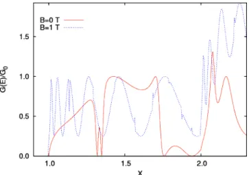
Of course the parabolic confinement of the wire always leads to the situation that at a high enough magnetic field the edge states will not be scattered by the quantum ring poten-tial, but now at an intermediate field strength the magnetic length compares more favorably with the size scale of the ring as can be seen in the conductance displayed in Fig. 15 for both B = 0 and 1 T.
At B = 1 T we see oscillations growing in wavelength with E or kn共E兲 both for mode n=0 and 1.
The oscillations in the conductance at B = 1 T are caused by a simple geometrical resonance where the wavelength of the scattering state in the ring has to compare appropriately with the circumference of the ring to build constructive or destructive interference, i.e., an Aharonov-Bohm-like effect. This also explains the growing wavelength of the oscillation with共E−E0兲. Even though the same condition lies at the root of the energy spectrum of stationary states in a ring in equi-librium we are not probing here the energy spectrum of the ring. We would like to mention that a similar oscillatory behavior of the conductance as a function of the energy was reported by Sivan et al.23 in the case of a quantum dot in
FIG. 9.共Color online兲 The probability density of the scattering stateE共x,y兲 in the parabolic quantum wire in the presence of an embedded quantum ring共Fig. 2兲, corresponding to the conductance in Fig. 6共b兲 at B=0.8 T. The incident energy X=1.933 共a兲 and 1.991
共b兲, corresponding to two minima in the conductance at the end of
the first step. FIG. 10. 共Color online兲 The conductance of a parabolic wire
with an embedded dot in units of G0= 2e2/ h. V1= 12 meV, V2= −18 meV, ប⍀0= 1.0 meV, 1aw2共B=0兲=3.412, 2aw2共B=0兲
high magnetic field. Since in high magnetic field the cyclo-tron radius is smaller than the ring radius one expects the electrons to travel within the ring along skipping orbits be-fore they leave through the wire.
The large size of the embedded ring in this case and its finite depth mean that quasibound states will not be of the same simple structure as seen for the smaller ring. This can be verified by the probability densities shown in Fig. 16 for the two dips at X = 1.319 and 1.347, and for the maximum at 1.425.
The total transmission of the only mode, n = 0, in Fig. 16共c兲 causes the perfect left-right symmetry, but the prob-ability density in Fig. 16共a兲 corresponding to the dip at X = 1.319 reflects the asymmetry caused by the confining parabolic potential to the ring seen in Fig. 14共b兲. The struc-ture of the evanescent states in Figs. 16共a兲 and 16共b兲 indi-cates that they are caused by states in the third and fifth energy bands and probably also states in higher bands. This persistence of eigenstates or scarring of wave functions in open systems has been discussed by Akis et al.24 for quan-tum dots, and here we confirm it for an open quanquan-tum ring. Superimposed on the Aharonov-Bohm-like oscillations in the conductance in Fig. 15 we have narrow resonances that are caused by interaction with quasibound states of the ring. In Fig. 17共a兲 we show the probability density for the scatter-ing state for a Aharonov-Bohm peak at X = 1.46. The density
FIG. 12.共Color online兲 The probability density of the scattering stateE共x,y兲 in the parabolic quantum wire in the presence of an
embedded quantum dot共Fig. 2兲, corresponding to the conductance in Fig. 10共a兲 at B=0.6 T for a state with incident energy X=2.235, in mode n = 0共a兲 and n=1 共b兲.
FIG. 13.共Color online兲 The probability density of the scattering stateE共x,y兲 in the parabolic quantum wire in the presence of an
embedded quantum dot共Fig. 2兲, corresponding to the conductance in Fig. 10共b兲 at B=1.2 T for a state with incident energy X=2.235, in mode n = 0共a兲 and n=1 共b兲.
FIG. 11.共Color online兲 The probability density of the scattering stateE共x,y兲 in the parabolic quantum wire in the presence of an
embedded quantum dot共Fig. 2兲, corresponding to the conductance in Fig. 10. The incident energy X = 1.679 at B = 0.6 T 共a兲 and
X = 1.557 at B = 1.2 T共b兲, corresponding to two minima in the
for a minimum in the oscillation is similar except for the addition of the reflected wave. In Fig. 17共b兲 we display the probability density for the first narrow resonance seen, at X = 1.135. Here we can identify a long lived evanescent state in the second subband.
IV. SUMMARY
We have successfully extended a multiband transport for-malism build on the Lippmann-Schwinger equation in a magnetic field to be able to describe an unbiased transport through a broad wire with embedded small or large quantum dots and rings defined by a smooth potential. The calculation of the probability density for the scattering states allows us to shed light on internal processes and resonances that in some cases reflect interaction between states in several sub-bands of the wire. We observe well known evanescent states and Fano resonances produced by these interactions. In the case of a large ring with finite width we observe Aharonov-Bohm type of oscillations superimposed with narrow reso-nances reflecting its energy spectrum.
Due to the wide range of system parameters used we had to pay extra attention to the accuracy of the numerical meth-ods employed.
FIG. 14. 共Color online兲 A contour plot of the potential of an embedded quantum ring in wire.共a兲 a ring with 1aw2= 3.41 and
2aw
2
= 11.37, corresponding to the ring in the upper panel of Fig. 2.
共b兲 A large ring with1aw
2共B=0兲=0.0682 and 2aw
2共B=0兲=0.682. E0=ប⍀w= 1.0 meV, aw= 33.7 nm at B = 0 T.
FIG. 15. 共Color online兲 The conductance of a parabolic wire with a large embedded ring关corresponding to Fig. 14共b兲兴 in units of G0= 2e2/ h. V
1= −12 meV, V2= 18 meV, ប⍀0= 1.0 meV, 1aw
2共B=0兲=0.0682,  2aw
2共B=0兲=0.682, and 13 subbands are
included.
FIG. 16.共Color online兲 The probability density of the scattering stateE共x,y兲 in the parabolic quantum wire in the presence of an embedded large quantum ring 关Fig. 14共b兲兴, corresponding to the conductance in Fig. 15 at B = 0 T for a state with incident energy
X = 1.319 corresponding to a dip 共a兲, X=1.347 in a dip 共b兲, and X = 1.425 at a maximum共c兲. The incoming mode is n=0.
ACKNOWLEDGMENTS
The research was partly funded by the Research and In-struments Funds of the Icelandic State, the Research Fund of the University of Iceland, and the National Science Council of Taiwan. C.S.T. acknowledges the computational facility supported by the National Center for High-Performance Computing of Taiwan. V.M. was supported by NATO.
APPENDIX A: PIECEWISE MATCHING OF MODES
To utilize the mode matching method, we divide the Gaussian scattering potential into a series of slices of width
␦L, each of them is described by a␦-profile potential Vsc共xi兲 = V0␦L exp共−xi
2兲␦共x − x
i兲. 共A1兲
As such, the Gaussian potential 共2兲 can be described by Vsc共r兲=兺i=1
NLV
sc共xi兲. For a right-going incident wave 共x,y,kn兲 from the nth mode of the left reservoir, the
corre-sponding scattering wave function can be expressed in the form n共i兲共x,y,kn兲 = eiknxn +共y,k n兲 +
兺
n⬘ rni⬘ne−ikn⬘x n⬘ − 共y,kn⬘兲 共A2兲 for x⬍xi, and n共i兲共x,y,kn兲 =兺
n⬘ tn ⬘n i e−ikn⬘x n⬘ +共y,k n⬘兲 共A3兲for x⬎xi. Following a similar procedure we can also obtain
the reflection and transmission coefficients r˜n ⬘n i
and t˜ni⬘nfor a left-going incident wave. Performing the piecewise matching at x = xi and multiplying these boundary conditions by the
eigenfunction m共y兲 of the ordinary unshifted harmonic
os-cillator with confining frequency⍀w, and integrating over y,
one obtains Eqs.共5兲 and 共6兲.
APPENDIX B: MATRIX ELEMENTS OF THE SCATTERING POTENTIAL
The matrix elements of the potential represented by a single Gaussian function V = V0exp共−xx2−yy2兲 is
accord-ing to Eqs.共19兲 and 共20兲 Vnn⬘共q,p兲 = V0aw
冑
x exp冋
−共q − p兲 2 4x册
Inn⬘共q,p兲, 共B1兲 where Inn⬘共q,p兲 =冕
dyn *共q,y兲e−yy2 n⬘共p,y兲. 共B2兲Insertion of the expressions for the eigenfunctions 共16兲 yields Inn⬘共q,p兲 = exp关共sn+ sn⬘兲2/4C −共sn 2+ s n⬘ 2兲/2兴 2n+n⬘
冑
Cn!n⬘
! ⫻p=0兺
n兺
q=0 n⬘冉
n p冊
⫻冉
n⬘
q冊
Hp共−冑
2sn兲Hp共−冑
2sn⬘兲 ⫻兺
l=0 min共n−p,n⬘−q兲 2ll!冉
n − p l冊冉
n⬘
− q l冊
⫻ bN/2−lH N−2l冉
z冑
2 bC冊
, 共B3兲 where N = n + n⬘
− p − q, sn= y0 n = knawc/⍀w, z =共sn+ sn⬘兲/ 共2冑
C兲, C=共1+yaw2兲, and b=共1−2/C兲. When the variable b assumes negative values the combination 共
冑
b兲N−2lHN−2l共¯/冑
b兲 still supplies the correct real value. FIG. 17.共Color online兲 The probability density of the scatteringstateE共x,y兲 in the parabolic quantum wire in the presence of an embedded large quantum ring 关Fig. 14共b兲兴, corresponding to the conductance in Fig. 15 at B = 1 T for a state with incident energy
X = 1.46 corresponding to a peak共a兲, and X=1.135 in a narrow dip 共b兲. The incoming mode is n=0.
1C. S. Chu and R. S. Sorbello, Phys. Rev. B 40, 5941共1989兲. 2P. F. Bagwell, Phys. Rev. B 41, 10 354共1990兲.
3V. Vargiamidis and O. Valassiades, J. Appl. Phys. 92, 302共2002兲. 4G. Cattapan and E. Maglione, Am. J. Phys. 71, 903共2003兲. 5J. Faist, P. Gueret, and H. Rothuizen, Phys. Rev. B 42, 3217
共1990兲.
6J. Bardarson, I. Magnusdottir, G. Gudmundsdottir, C. Tang, A.
Manolescu, and V. Gudmundsson, Phys. Rev. B 70, 245308
共2004兲.
7S.-X. Qu and M. R. Geller, Phys. Rev. B 70, 085414共2004兲. 8Y. Takagaki and K. Ploog, Phys. Rev. B 51, 7017共1995兲. 9S. A. Gurvitz, Phys. Rev. B 51, 7123共1995兲.
10A transfer-matrix method was discussed by C. C. Wan, T. De
Jesus, and H. Guo, Phys. Rev. B 57 11 907共1998兲.
11A scattering-matrix method was discussed by H. Xu, Phys. Rev. B
50, 8469共1994兲.
12C. S. Tang and C. S. Chu, Physica B 292, 127共2000兲.
13J. H. Bardarson, MS thesis, University of Iceland, 2004, available
at http://www.raunvis.hi.is/reports/2004/RH-09-2004.html.
14M. I. Haftel and F. Tabakin, Nucl. Phys. A 158, 1共1970兲.
15R. H. Landau, Quantum Mechanics II: A Second Course in Quan-tum Theory, 2nd ed.共John Wiley & Sons, Inc., 1996兲.
16C. S. Tang, Y. H. Tan, and C. S. Chu, Phys. Rev. B 67, 205324 共2003兲.
17U. Fano, Phys. Rev. 124, 1866共1961兲.
18J. A. Simpson and U. Fano, Phys. Rev. Lett. 11, 158共1963兲. 19S. A. Gurvitz and Y. B. Levinson, Phys. Rev. B 47, 10 578
共1993兲.
20J. Göres, D. Goldhaber-Gordon, S. Heemeyer, M. A. Kastner, H.
Shtrikman, D. Mahalu, and U. Meirav, Phys. Rev. B 62, 2188
共2000兲.
21K. Kobayashi, H. Aikawa, S. Katsumoto, and Y. Iye, Phys. Rev.
Lett. 88, 256806共2002兲.
22K. Kobayashi, H. Aikawa, S. Katsumoto, and Y. Iye, Phys. Rev. B
68, 235304共2003兲.
23U. Sivan, Y. Imry, and C. Hartzstein, Phys. Rev. B 39, 1242 共1989兲.
24R. Akis, J. P. Bird, and D. K. Ferry, Appl. Phys. Lett. 81, 129 共2002兲.