Threshold current density of electromigration in eutectic SnPb solder
Y. T. Yeh, C. K. Chou, Y. C. Hsu, Chih Chen, and K. N. Tu
Citation: Applied Physics Letters 86, 203504 (2005); doi: 10.1063/1.1929870
View online: http://dx.doi.org/10.1063/1.1929870
View Table of Contents: http://scitation.aip.org/content/aip/journal/apl/86/20?ver=pdfcov Published by the AIP Publishing
Articles you may be interested in
Relationship between edge drift and atomic migration during electromigration of eutectic SnPb lines J. Appl. Phys. 100, 033715 (2006); 10.1063/1.2210262
Electromigration and critical product in eutectic SnPb solder lines at 100 ° C J. Appl. Phys. 100, 024909 (2006); 10.1063/1.2216487
Critical length of electromigration for eutectic SnPb solder stripe Appl. Phys. Lett. 88, 182105 (2006); 10.1063/1.2200158
Redistribution of Pb-rich phase during electromigration in eutectic SnPb solder stripes J. Appl. Phys. 99, 054502 (2006); 10.1063/1.2178392
Electromigration in eutectic SnPb solder lines J. Appl. Phys. 89, 4332 (2001); 10.1063/1.1357459
This article is copyrighted as indicated in the article. Reuse of AIP content is subject to the terms at: http://scitation.aip.org/termsconditions. Downloaded to IP: 140.113.38.11 On: Thu, 01 May 2014 03:02:18
Threshold current density of electromigration in eutectic SnPb solder
Y. T. Yeh, C. K. Chou, Y. C. Hsu, and Chih Chena兲Department of Material Science and Engineering, National Chiao Tung University, Hsin-chu 300, Taiwan, Republic of China
K. N. Tu
Department of Materials Science and Engineering, University of California, Los Angeles, California 90095-1595
共Received 2 December 2004; accepted 5 April 2005; published online 12 May 2005兲
Electromigration has emerged as an important reliability issue in the microelectronics packaging industry since the dimension of solder joints has continued to shrink. In this letter, we report a technique that enables the precise measurement of the important parameters of solder electromigration, such as activation energy, critical length, threshold current density, effective charge numbers, and electromigration rate. Patterned Cu/ Ti films in a Si trench were employed for eutectic SnPb solder to be reflowed on, and thus solder Blech specimens were fabricated. Atomic force microscope was used to measure the depletion volume caused by electromigration on the cathode end. The threshold current density is estimated to be 8.5⫻103A / cm2 at 100 °C, which
relates directly to the maximum allowable current that a solder joint can carry without electromigration damage. This technique facilitates the scientifically systematic investigation of electromigration in solders. © 2005 American Institute of Physics. 关DOI: 10.1063/1.1929870兴 The rapid growth of microelectronic technology has
been based on the constant reduction in cost per transistor, together with increased performance. Along with the trend of miniaturization, electronic packaging of a Si chip that has a very-large-scale-integration of circuits requires a very large number of input/output共I/O兲 connections on the packaging substrate. Flip chip technology with area array of solder bumps has become the most important packaging technology to achieve high-density packaging. The size of these solder bumps is quite small, with a diameter of about 100m or less.1,2 The design rule for packaging requires that each bump will carry 0.2–0.4 A. Under a high current density, a common cause of failure in interconnects is “electromigra-tion,” which is the enhanced diffusion of atoms in the current direction due to electron momentum transfer to a diffusing atom.3
From the point of view of device reliability, electromi-gration in a flip chip solder joint is as significant as that in Al or Cu interconnect line because of the high lattice diffusivity in the solder alloys, together with higher resistivity, lower Young’s modulus, and higher effective charge number of the chemical elements in solder alloys than those of Al or Cu.3–8 It is known that the current density needed to cause a solder joint to fail is about two orders of magnitude less than that to cause an Al or Cu line to fail.4,6However, one of the funda-mental parameters of electromigration, the critical length of solder joint, has not been measured or estimated.
In general, the atomic flux of electromigration “JEM” in a
conductor driven by a constant current density “j” can be expressed as the following:3
JEM= CDZ*eE = C
冉
D0 kT冊
exp冉
− Ea kT冊
Z *ej,where JEMis the electromigration flux, C is the concentration
of atoms per unit volume of the eutectic alloy, D is the
ef-fective lattice diffusivity of the solder at testing temperature,
Z*is the effective charge number, E is the electric field, D 0is
the prefactor for the diffusivity, Ea is the activation energy
for electromigration, is resistivity of the film, k is the Boltzmann’s constant, and T is the absolute temperature. Among these factors, Z* is the most important parameter in electromigration.
Blech developed a short stripe technique for measuring
Z*, provided that the length of the stripe is longer than a critical length.4The “critical length” is defined by the length in which the electromigration flux is balanced by an oppos-ing flux due to the back stress gradient induced by the elec-tromigration. The critical length can be measured from a set of stripes longer than the critical length and tested under a constant current density or from stripes of a given length but tested at various current densities. Electromigration will cause depletion at the cathode end of the stripe. Measuring the depletion length and time, we obtain the draft velocity. Thus, the threshold or critical current density corresponding
a兲Author to whom correspondence should be addressed; electronic mail: [email protected]
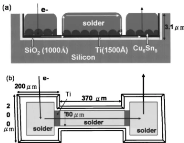
FIG. 1. The schematics of solder Blech specimens.共a兲 Cross-sectional dia-gram of the solder strip inside the Si trench.共b兲 Plan-view diagram of the solder strip on the Cu/ Ti metallization layer. The SnPb strip is 370m long, 80m wide, and approximately 3m thick.
APPLIED PHYSICS LETTERS 86, 203504共2005兲
0003-6951/2005/86共20兲/203504/3/$22.50 86, 203504-1 © 2005 American Institute of Physics
This article is copyrighted as indicated in the article. Reuse of AIP content is subject to the terms at: http://scitation.aip.org/termsconditions. Downloaded to IP: 140.113.38.11 On: Thu, 01 May 2014 03:02:18
to the critical length can be obtained by extrapolating to the zero drift velocity.
When solder joints are stressed by a current density of 5⫻103A / cm2 and above, electromigration occurs even at room temperature.5–12 The electromigration rates in Pb-containing solders were measured by applying currents in thin strips of solder lines joined with Cu electrodes. The effective charge number of eutectic SnPb solder was mea-sured to be 33 for a fixed length of V-groove solder lines stressed by 2.8⫻104 A / cm2 at 150 °C.8 However, no mea-surement of electromigration in a Blech stripe of SnPb solder has been done because the evaporation of lead is toxic, so we cannot use deposition methods to fabricate Blech stripes of Pb-based alloys as Al stripes. In this letter, we report a tech-nique to fabricate solder Blech specimens, in which the depletion volume caused by electromigration and the drift velocity can be measured precisely. The electromigration rate for various current densities at 100 °C and the threshold cur-rent density of eutectic SnPb solder are reported in this letter. To fabricate the solder Blech specimens, trenches of about 3.1m deep were etched in a 共001兲 Si wafer by deep reactive ion etcher, and an oxide layer of 100 nm was grown on the Si wafer for electric insulation. Then 0.12m Ti film was deposited on the oxide surface, followed by 0.4m Cu film deposition using e-beam evaporator. Then, photolithog-raphy and selective etching were employed to pattern the Cu layer. The wafer was cut into small pieces of about 5 mm ⫻5 mm squares. They were polished to remove the Cu/Ti metallization layer on the top Si surface, leaving the metal-lization layers in the trench intact.
Afterwards, SnPb solder paste was positioned in the trenches, and they were reflowed at 210 °C for 4 s on a hot plate. Since the molten solder wets only the Cu surface, sol-der Blech specimens were formed automatically after the re-flow. Nevertheless, the shape of the solder became bump-like due to its surface tension during the reflow process. A second polishing was needed to obtain a flat and smooth surface. The Si trench served as a polish stop, since SnPb is known to be very soft. Thus the thickness of the solder strip can be controlled by the polishing. The schematic of the specimen is illustrated in Fig. 1. Figure 1共a兲 depicts the cross-sectional view of the solder strip inside the Si trench. The thickness of the solder stripe is controlled by the depth of the trench. When electrical currents are applied through the electrode pads, the electron path is indicated by the arrows in the fig-ure. Figure 1共b兲 depicts the plan view of the specimen. The dimension of the SnPb strip is 370m long, 80m wide, and 3.1m thick. The pads are squares of about 200m ⫻200m.
Figure 2 depicts the schematic structure of bump pairs, in which the electrons in the Al trace crowd into a solder bump after passing through the intermetallic compound 共IMC兲 layer, flowing inside the solder bump, and then drift into the Cu line after the passage of another IMC layer. Typi-cally, electromigration failure occurs at the junction of the Al trace and the bump, where current crowding takes place.2 The path of electrons in the Blech specimen is quite similar to that in the flip chip solder bump. Thus, the measured elec-tromigration rate in the Blech specimen may be close to that in flip chip solder bumps. Furthermore, the Cu metallization layer could be changed to Ni, since Ni is another important metallization film for flip chip solder bumps. The effect of metallization layer and IMC on electromigration can be in-vestigated using these specimens.
To measure threshold current density for SnPb solder, various current densities ranging from 3⫻104 to 1
⫻105A / cm2 were applied to the specimen by probing the
two pads on a probe station with a hot stage at 100 °C. The current densities refer to the average ones drifting in the solder strips. The depletion volume on the cathode end was measured before and after the current stressing. However, due to the softness of the solders, the edge of the solder was not abrupt after the above-noted sample preparation proce-dures. Therefore, the depletion volume could not be mea-sured accurately by scanning electron microscope 共SEM兲
FIG. 2. Schematic structure for a pair of solder bumps, in which the elec-trons in the Al trace crowd into the left solder bump after passing through the IMC layer, flowing inside the solder bump, and then drift into the Cu line after the passing into another IMC layer.
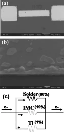
FIG. 3. SEM images for a fabricated Blech specimen.共a兲 The plan view image, in which the SnPb solder strip and the two pads are labeled.共b兲 The cross-sectional image of the solder stripe is共a兲. The average thickness of the IMC layer is 0.6m.共c兲 The effective circuit for the tri-layered Blech structure. Around 80% of the applied current drifted in the solder.
203504-2 Yehet al. Appl. Phys. Lett. 86, 203504共2005兲
This article is copyrighted as indicated in the article. Reuse of AIP content is subject to the terms at: http://scitation.aip.org/termsconditions. Downloaded to IP: 140.113.38.11 On: Thu, 01 May 2014 03:02:18
alone. To overcome this difficulty, atomic force microscope 共AFM兲 was employed to scan the region near the cathode end before and after the stressing, so that the depletion vol-ume could be estimated precisely. The AFM used in this study was DI Nanoscope E.
Figure 3共a兲 shows the plan-view SEM image for a fab-ricated Blech specimen, in which the SnPb solder strip and the two pads are labeled. The cross-sectional SEM image of the solder strip is seen in Fig. 3共b兲. An IMC of Cu6Sn5
formed between the SnPb solder and the Cu metallization layer. The thicknesses of the solder, IMC, and remaining metallization were measured to be 2.4, 0.6, and 0.1m, re-spectively. Therefore, when the electrons drift in the solder
outside the crowding area, they encounter an effective cir-cuit, as shown in Fig. 3共c兲. As can be seen, around 80% of the applied current drifts in the solder strip, 19% in the IMC layer, and only 1% in the Ti layer.
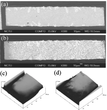
Upon current stressing, depletion of solder occurred on the cathode end and extrusion formed on the anode end of the solder strip, as seen in Figs. 4共a兲 and 4共b兲. Figure 4共a兲 shows the plan-view SEM image of another SnPb solder strip before current stressing, in which the brighter region represents the Pb-rich phase and the darker region corre-sponds to the Sn-rich phase. After the current stressing of 6.9⫻104A / cm2 at 100 °C for 34.7 h, its microstructure is shown in Fig. 4共b兲. Depletion of solder occurred at the cath-ode end due to electromigration, causing the IMC to be vis-ible from a top view. On the other hand, irregular extrusions of solder were observed on the anode side. To measure the depletion volume for calculating drifting velocity, AFM scanning was performed to obtain three-dimensional surface profiles before and after the current stressing, as seen in Figs. 4共c兲 and 4共d兲, respectively. By estimating the volume differ-ence between the two profiles, depletion volume and thus drift velocity were acquired.
Figure 5 shows the measured drift velocity as a function of applied current density at 100 °C. The drift velocity in-creases when the applied current inin-creases. By extrapolating to the zero drift velocity, the estimated threshold current den-sity is obtained as 8.5⫻103A / cm2. This value represents
the maximum current density that the solder can carry with-out electromigration damage at device operation temperature of 100 °C. To verify if this extrapolated value is accurate, another specimen was stressed at the current density of 5 ⫻103A / cm2at 100 °C for 100 h, and no detectable volume
change was found.
In summary, we have successfully developed a technique that can measure precisely the important parameters of solder electromigration. Solder Blech specimens were fabricated on patterned Cu/ Ti films in Si trenches. By employing AFM to measure the depletion volume on the cathode end, the elec-tromigration rate can be measured. The threshold current density was estimated to be 8.5⫻103 A / cm2 at 100 °C.
The authors would like to thank the National Science Council of the R.O.C. for financial support of this study through Grant No. 91-2216-E-009-032.
1
The International Technology Roadmap for Semiconductor共2003兲.
2
K. N. Tu, J. Appl. Phys. 94, 5451共2003兲.
3
H. B. Huntington and A. R. Grone, J. Phys. Chem. Solids 20, 76共1961兲.
4
I. A. Blech, J. Appl. Phys. 47, 1203共1976兲.
5
S. Brandenburg and S. Yeh, Proceedings of Surface Mount International Conference and Exhibition, SM198, San Jose, CA, 23–27 August 1998 共Edina, MN, SMTA, 1998兲, p. 337.
6
C. Y. Liu, C. Chen, C. N. Liao, and K. N. Tu, Appl. Phys. Lett. 75, 58
共1999兲.
7
C. Y. Liu, C. Chen, and K. N. Tu, J. Appl. Phys. 88, 5703共2000兲.
8
Q. T. Huynh, C. Y. Liu, C. Chen, and K. N. Tu, J. Appl. Phys. 89, 4332
共2001兲.
9
J. D. Wu, P. J. Zheng, Kelly Lee, C. T. Chiu, and J. J. Lee, 2002 Electronic Components and Technology Conference, p. 452.
10
J. W. Nah, K. W. Paik, J. O. Suh, and K. N. Tu, J. Appl. Phys. 94, 7560
共2003兲.
11
T. Y. Lee, K. N. Tu, S. M. Kuo, and D. R. Frear, J. Appl. Phys. 89, 3189
共2001兲.
12
J. K. Lin. J. W. Jang, and J. White, 2003 Electronic Components and Technology Conference, p. 816.
FIG. 4. 共a兲 Plan-view SEM image of a SnPb solder strip before current stressing, in which the brighter region represents the Pb-rich phase and the darker region corresponds to the Sn-rich phase.共b兲 The solder strip in 共a兲 after the current stressing of 6.9⫻104A / cm2at 100 °C for 34.7 h.共c兲 AFM
image of the cathode end of the solder strip in共a兲. 共d兲 AFM image of the cathode end of the solder strip in共b兲.
FIG. 5. The measured drift velocity as a function of applied current density at 100 °C. The calculated threshold current density is 8.5⫻103A / cm2by
extrapolating to the zero drift velocity.
203504-3 Yehet al. Appl. Phys. Lett. 86, 203504共2005兲
This article is copyrighted as indicated in the article. Reuse of AIP content is subject to the terms at: http://scitation.aip.org/termsconditions. Downloaded to IP: 140.113.38.11 On: Thu, 01 May 2014 03:02:18