行政院國家科學委員會補助專題研究計畫
■ 成 果 報 告
□期中進度報告
以熱溶劑合成法製備一維奈米材料之異質結構
計畫類別:■ 個別型計畫 □ 整合型計畫
計畫編號:NSC 96-2218-E-009-007
執行期間:96 年 08 月 01 日至 97 年 07 月 31 日
執行單位:國立交通大學 材料科學與工程學系
計畫主持人:徐雍鎣
成果報告類型(依經費核定清單規定繳交):□精簡報告 ■完整報告
本成果報告包括以下應繳交之附件:
□赴國外出差或研習心得報告一份
□赴大陸地區出差或研習心得報告一份
■出席國際學術會議心得報告及發表之論文各一份
□國際合作研究計畫國外研究報告書一份
處理方式:本計畫可公開查詢
中 華 民 國 97 年 10 月 26 日
行政院國家科學委員會專題研究計畫成果報告
摻雜物引導成長之硫化鎘四足狀奈米結構
Dopant-Induced Formation of Nanosized CdS Tetrapods
計畫編號:NSC-96-2218-E-009-007
執行期限:96 年 08 月 01 日至 97 年 07 月 31 日
主持人:徐雍鎣 交通大學材料系
Abstract
CdS tetrapods of high morphological yields can be obtained with a simple solvothermal process by simply incorporating Se or Te as dopant in the process. It is proposed for the first time that dopant Se or Te can kinetically transform the growth habit of CdS nuclei from the typical wurtzite (WZ) to zinc blende (ZB) phase, thus making the formation of multi-armed structures much easier. Upon addition of Se or Te, CdS turns to nucleate in ZB phase, instead of the typical WZ phase, from which the subsequent one-dimensional growth of WZ arms leads to the formation of the tetrapods. The doping inducement effect on the tetrapod/tripod formation may give new insights into the manipulation and controllability of anisotropic nanocrystal growth. The present finding can be readily extended to other semiconductors possessing ZB-WZ polymorphism.
關鍵字:cadmium sulfide (硫化鎘), crystal growth (晶體成長), doping (摻雜)
1. Introduction
Tetrapods, a unique example of these anisotropically-shaped NCs, find potential applications in nanocomposites and nano-scale devices. For example, because of the three-dimensionally extending structures, tetrapods may be a promising building unit for preparation of interesting superstructures for nano-electronics, especially three-dimensional (3D) prototypes.[1] In addition, semiconductor tetrapods have potential advantages in hybrid NC/polymer photovoltaic devices because their 3D structures make it facile for them to orderly align toward the electrodes within the polymer film, providing direct charge carrier transportation pathway to improve the device performance.[2] The most often observed crystallographic feature of these tetrapod NCs is one cubic zinc blende (ZB) core attached with four hexagonal wurzite (WZ) arms. Evidently, to form such novel architecture, one should have the crystals nucleate in ZB phase followed by anisotropic growth in WZ phase. The ability of crystals to switch from one growth mode to another during a continuous reaction is thus crucial to achieving the tetrapod
growth. Here, we report a novel approach to facilitate the formation of CdS tetrapods by simply incorporating a trace amount of dopants in a solvothermal process. The crystallographic structure of the tetrapods was examined with a high-resolution transmission electron microscope (HRTEM), which showed that the tetrapod had a ZB core and four WZ arms. A plausible mechanism for the tetrapod growth was proposed and discussed.
2. Experimental Section
The syntheses of nanowires, Se-doped tetrapods, and Te-doped tetrapods of CdS were carried out in a solvothermal process. For the preparation of CdS NWs, Cd(NO3)2·4H2O (1.85 g, 0.006 moles) and S powder (0.19 g, 0.006 moles) were added to an ethylenediamine (EN, 100 ml) containing flask (250 ml). After a 5 min stirring, the solution turned straw-yellow, and the solution was transferred to a teflon-lined stainless steel autoclave (with a capacity of 120 ml). The autoclave was sealed, heated, and maintained at 180oC for 24 hrs. For the synthesis of Se-doped CdS tetrapods, Cd(NO ) ·4H O (1.85 g, 0.006 moles), S
powder (0.32 g, 0.01 moles), and Se powder (0.079 g, 0.001 moles) were used as the precursors, followed by the same procedure performed in the synthesis of CdS NWs. As to the fabrication of Te-doped tetrapods, Cd(NO3)2·4H2O (1.85 g, 0.006 moles), S powder (0.32 g, 0.01 moles), and Te powder (0.128 g, 0.001 moles) were used, followed by the same reaction procedure mentioned above.
3. Results and Discussion
The structures and dimensions of the as-prepared products were first investigated with scanning electron microscope (SEM). Figure 1(a) shows the SEM image of CdS nanowires (NWs) obtained under the typical solvothermal reaction with Cd(NO3)2 and S powder as the reactants and ethylenediamine (EN) as the solvent. The growth of CdS NWs was guided by the capping effect of the EN present in the system. With extra feeding of a trace amount of Se powder in the reactants while keeping all other reaction parameters fixed, multi-branched structures became the dominant product instead of NWs, as can be seen in Figure 1(b). These branched structures (tetrapods) remained dominant with high morphological yields if Te powder was fed along with the S powder as the dopant. The average diameters of the NWs and branched arms were about 30 nm. The arm length of these tetrapods varied from 100 to 700 nm. The atomic compositions of Se and Te in the tetrapod products were around 5% and 2.5%, respectively, as determined from the TEM-EDS analyses. The crystallographic structures of the as-synthesized samples were further characterized with X-ray diffraction (XRD) and HRTEM.
Figure 1(d) shows the XRD patterns of the three CdS-based nanostructures. All three samples show predominantly the diffraction behaviour of WZ CdS. For CdS NWs, the diffraction peak at 2θ of 26.5o corresponds well to the WZ-(0002) planes with a d-spacing of 0.336 nm, as determined from Bragg’s law. For the Se-doped and Te-doped samples, the 2θ of around 26.3o gives an interplanar spacing of 0.339 nm for the WZ-(0002) planes. The slight expansion of the lattice in doped samples was
due to the partial replacement of S with Se or Te atoms which are of larger atomic size. The detailed crystal structures of the as-synthesized samples were analyzed with HRTEM. Figure 2 shows the HRTEM images of an individual NW, Se-doped tetrapod, and Te-doped tetrapod of CdS. Interplanar spacings of 0.67, 0.68, and 0.68 nm were observed in the axial directions of the NW and tetrapod arms of the Se-doped and Te-doped samples, respectively. The lattice spacings were in good agreement with the d-spacings of the WZ-(0001) planes, as determined from the corresponding XRD analyses. The axis of the NW is parallel with the WZ-[0001] direction, indicating the NWs were grown along the c-axis. Furthermore, the four arms of the Se-doped or Te-doped tetrapods also possessed a preferential crystalline direction along the WZ-[0001].
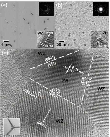
The most common structural feature of an artificially synthesized tetrapod is a ZB core possessing of four {111} facets, each attached with a WZ arm growing along the [0001] direction. In other words, tetrapods are formed when nanocrystals nucleate in ZB phase first, followed by growth of WZ arms from the four equivalent ZB-(111) facets of the tetrahedral ZB core. For the present work, we show that the same growth mechanism applies for the formation of the present Se-doped or Te-doped CdS tetrapods. To give a solid proof of the claim, we examined the phase of the cores at the core formation stage. By suitably controlling the experimental conditions, the solvothermal reaction can be terminated at the early stage of the nanocrystal growth. The TEM images shown in Figures 3(a) and (b) give a clear illustration on the following points. For reactions with only S powder as the chalcogen source, CdS nucleated in its most stable WZ phase and grew into short nanorods along a preferential crystalline planes of (0001) which possess the smallest surface energy among all growing planes.[3] With the incorporation of Se or Te in the reaction, nanocrystals of CdS however tended to nucleate in ZB phase to form nanoparticles, instead of nanorods. The ZB phase of these nanoparticles can be identified from the spacing of lattice fringes and the electron diffraction pattern shown in
the two insets of Figure 3(b). The existence of the ZB phase in the resulting tetrapod can be further confirmed by the HRTEM image shown in Figure 3(c), taken on the intersectional region of a tripod. An evident difference in lattice fringes between the core region and the three arms was revealed, indicating distinct crystal phases therein. The lattice fringes of the three {111} facets imply that the ZB core can be attached with four arms leading to a tetrahedral structure. The three arms show a 0.34 nm interlayer spacing, which can be indexed as the spacing in the WZ-[0001] direction. The lattice-matched planes between the ZB core and the WZ arms imply an epitaxial relationship. From the results presented above, it can be concluded that the Se-doped and Te-doped CdS tetrapods obtained in this work possessed a ZB core, with WZ arms grown out of the equivalent {111} facets of the ZB core.
There have been developed quite a few approaches for preparation of nanosized semiconductor tetrapods. Most of them are based on the growth energy difference between ZB and WZ phases, through which the nanocrystal growth can switch from one phase to another. Typically, through suitably controlling the temperature of growth,[4] the concentration of precursors,[5] or by applying specific capping ligands in the reaction,[6] tetrapod nanocrystals can be obtained in single-step processes. Besides, a two-step sequential growth technique, in which the first-prepared ZB core served as the seeds for the subsequent growth of WZ arms, can also generate this architecture. For the CdTe case, the energy difference between ZB and WZ phases is appropriately large[7] to enable easy controls over the growth of ZB core and WZ arms to form tetrapod nanocrystals. However, it has been pointed out that this energy difference is too small to facilitate controllable tetrapod formation for CdS, CdSe, and ZnS.[2a] In our experiments, we found that it was the incorporation of dopant Se or Te that caused the formation of CdS tetrapods through increasing the energy difference between the two phases. Note that the energy difference for II-VI
semiconductors between WZ and ZB phases increases monotonically as the anions become larger in atomic size.[7] It is thus reasonable that upon incorporation of Se or Te atoms, the growth energy difference between ZB and WZ phases for CdS is significantly enlarged. As a result, the growth of starting ZB seeds and subsequent WZ arms can proceed in a single-pot process.
A plausible growth mechanism for the formation of Se-doped and Te-doped CdS tetrapods is proposed as follows. At the beginning of the reaction, Se and Te incorporation resulted in the growth of CdS nuclei in ZB phase with four equivalent {111} facets exposed, as evident from the HRTEM image shown in Figure 3(b). The first formed ZB CdS nanoparticles then served as the seeds for the WZ arms to grow from them. The arm diameter of the resulting tetrapods may be adjusted by controlling the size of the ZB seeds. Note that the lattice arrangement of Cd and S atoms on the {111} planes of ZB phase are identical to those on the WZ-(0001) plane.[5a] Furthermore, the {111} planes in ZB CdS are epitaxially matched with the WZ-(0002) planes due to the closeness in their d-spacings (dZB(111)≒dWZ(0002)=0.34 nm). Both the atomic arrangement and lattice spacing matches contributed to the CdS tetrapod formation of this work. The solvent EN also played an important role here. In a typical case, WZ CdS NWs grew with a preferential direction along the c-axis under the inducement of EN.[8] In this situation, EN tended to attach to the {10-10} planes and suppress the growth rate of these planes, while the (0001) planes, covered with the least amount of EN, grew the fastest. Thus, it was the different adsorption ability of EN toward different planes of CdS nanocrystals that made the one-dimensional growth of WZ arms possible. By suitably controlling the synthetic conditions, such as reaction temperature, heating rate, and reactant concentration, it is possible to reduce the arm diameter of the tetrapod-shaped nanocrystals. This task can be achieved
through effective modulation of the size of the ZB seeds grown at the early stage of the solvothermal process as well as through manipulation of relevant growth kinetics of CdS as that proposed by Manna et al.[2a] In an ideal situation, totally identical arms should be obtained in the resulting tetrapods. However, because of the inevitable local concentration fluctuations existing in the reacting system, non-equilateral arm growth may take place and even worse the growth of one or even more arms may be completely suppressed, leading to possible appearance of three- and two-armed structures. As a final note, the Ostwald ripening effect, in which longer arms grow even longer at the expense of shorter ones, also contributed to the unequal arm lengths observed as shown in Figures 2(b) and (c).
4. Conclusion
In conclusion, CdS tetrapods of high morphological yields can be obtained with a simple solvothermal process by simply incorporating Se or Te as dopant in the process. It is proposed for the first time that dopant Se or Te can kinetically transform the growth habit of CdS nuclei from the typical WZ to ZB phase, thus making the formation of multi-armed structures much easier. The doping inducement effect on the tetrapod formation may give new insights into the manipulation and controllability of anisotropic nanocrystal growth. The present finding can be readily extended to other semiconductors possessing ZB-WZ polymorphism.[10]
References
[1] a) H. T. Liu, A. P. Alivisatos, Nano Lett. 2004, 4, 2397-2401. b) D. J. Milliron, S. T. Hughes, Y. Cui, L. Manna, J. Li, L.-W. Wang, A. P. Alivisatos, Nature 2004, 430, 190-195. c) Y. Cui, U. Banin, M. T. Björk, A. P. Alivisatos, Nano Lett. 2005, 5, 1519-1523. d) D. Tarì, M. D. Giorgi, F. D. Sala, L. Carbone, R. Krahne, L. Manna, R. Cingolani, Appl. Phys. Lett. 2005, 87, 224101.
[2] a) L. Manna, D. J. Milliron, A. Meisel, E. C. Scher, A. P. Alivisatos, Nat. Mater. 2003, 2, 382-385. b) B. Q. Sun, E. Marx, N. C. Greenham, Nano Lett. 2003, 3, 961-963. c) E. C. Scher, L. Manna, A. P. Alivisatos, Philos. Trans. R. Soc. London, Ser. A 2003,
361, 241-257. d) I. Gur, N. A. Fromer, A. P. Alivisatos, J. Phys. Chem. B 2006, 110, 25543-25546.
[3] a) G. Shen, C.-J. Lee, Cryst. Growth Des. 2005, 5, 1085-1089. b) Y.-F. Lin, Y.-J. Hsu, S.-Y. Lu, S.-C. Kung, Chem. Commun. 2006, 2391-2393.
[4] a) Y. W. Jun, S. M. Lee, N. J. Kang, J. Cheon, J. Am. Chem. Soc. 2001, 123, 5150-5151. b) M. Chen, Y. Xie, J. Lu, Y. J. Xiong, S. Y. Zhang, Y. T. Qian, X. M. Liu, J. Mater. Chem. 2002, 12, 748-753. c) H. Chu, X. Li, G. Chen, W. Zhou, Y. Zhang, Z. Jin, J. Xu, Y. Li, Cryst. Growth Des. 2005, 5, 1801-1806.
[5] a) L. Manna, E. C. Scher, A. P. Alivisatos, J. Am. Chem. Soc. 2000, 122, 12700-12706. b) J. W. Grebinski, K. L. Hull, J. Zhang, T. H. Kosel, M. Kuno, Chem. Mater. 2004, 16, 5260-5272.
[6] a) S. D. Bunge, K. M. Krueger, T. J. Boyle, M. A. Rodriguez, T. J. Headley, V. L. Colvin, J. Mater. Chem. 2003, 13, 1705-1709. b) W. W. Yu, Y. A. Wang, X. G. Peng, Chem. Mater. 2003, 15, 4300-4308. c) L. Carbone, S. Kudera, E. Carlino, W. J. Parak, C. Giannini, R. Cingolani, L. Manna, J. Am. Chem. Soc. 2006, 128, 748-755. [7] C.-Y. Yeh, Z. W. Lu, S. Froyen, A. Zunger, Phys. Rev. B 1992, 46, 10086–10097.
[8] a) Y. D. Li, H. W. Liao, Y. Ding, Y. Fan, Y. Zhang, Y. T. Qian, Inorg. Chem. 1999, 38, 1382-1387. b) J. Yang, J.-H. Zeng, S.-H. Yu, L. Yang, G.-E. Zhou, Y.-T. Qian, Chem. Mater. 2000, 12, 3259-3263. c) D. Xu, Z. Liu, J.o Liang, Y.Qian, J. Phys. Chem. B 2005, 109, 14344-14349.
Figure 1. SEM images of (a) CdS NWs, (b) Se-doped CdS tetrapods, and (c) Te-doped CdS tetrapods. (d) XRD patterns of the as-synthesized samples with the reference hexagonal CdS
(JCPDS # 06-0314) included for comparison.
Figure 2. Typical TEM images of an individual (a) CdS NW, (b) Se-doped CdS tetrapod, and (c) Te-doped CdS tetrapod. Their corresponding lattice-resolved images are shown in (d), (e), and (f),
Figure 3. TEM images of (a) WZ CdS and (b) ZB Te-doped CdS nanocrystals obtained at the early stage of the solvothermal process. The insets show their corresponding SAED and HRTEM images. (c) An HRTEM image taken on the intersectional region (as marked in the inset) of a Te-doped CdS tripod. The interfaces between the ZB core and the WZ arms are highlighted with the dashed lines.
計畫成果自評
1. 在合成一維 CdS 奈米線異質結構之研究上,利用外加摻雜物(Se 與 Te)於熱溶劑成長系統 中,可進一步改變CdS 晶體之成核與成長模式,成功製備 Se-doped CdS 與 Te-doped CdS 之奈米四足狀結構,此四足狀奈米結構可應用於光電傳輸元件上。(published in Small 2008, 4, 951-955) 2. 以熱溶劑法所製備之 CdS 奈米線,其表面所具有之官能基(乙二胺)可被用於還原金屬離 子,並成長金屬奈米顆粒於奈米線表面,以形成金屬/半導體奈米線之異質結構,此異質 結構可應用於光觸媒與光電池元件上。(published in Chem. Mater. 2008, 20, 2854-2856) 3. 於化學氣相沈積系統中,成功製備 Mn 原子摻雜之半導體 CdSe 奈米線,係所謂稀磁性半導體奈米線,此複合奈米線於室溫下展現出超順磁性質,可乃具有發展為生物磁性標誌劑 與生物磁性顯影劑之用途。(published in J. Phys. Chem. C 2008, in press)
4. 我們已達成預期的研究成果。
5. 此研究計畫之研究成果已發表在頂級國際期刊 Small (SCI IF: 6.408)、Chem. Mater. (SCI IF: 4.883)與 J. Phys. Chem. C.。