Research Article
Void Shapes Controlled by Using Interruption-Free
Epitaxial Lateral Overgrowth of GaN Films on Patterned SiO
2
AlN/Sapphire Template
Yu-An Chen, Cheng-Huang Kuo, Li-Chuan Chang, and Ji-Pu Wu
Institute of Lighting and Energy Photonics, National Chiao Tung University, Tainan 71150, TaiwanCorrespondence should be addressed to Cheng-Huang Kuo; [email protected]
Received 20 February 2014; Revised 26 April 2014; Accepted 2 June 2014; Published 18 June 2014 Academic Editor: Nelson Tansu
Copyright © 2014 Yu-An Chen et al. This is an open access article distributed under the Creative Commons Attribution License, which permits unrestricted use, distribution, and reproduction in any medium, provided the original work is properly cited. GaN epitaxial layers with embedded air voids grown on patterned SiO2AlN/sapphire templates were proposed. Using interruption-free epitaxial lateral overgrowth technology, we realized uninterrupted growth and controlled the shape of embedded air voids. These layers showed improved crystal quality using X-ray diffraction and measurement of etching pits density. Compared with conventional undoped-GaN film, the full width at half-maximum of the GaN (0 0 2) and (1 0 2) peaks decreased from 485 arcsec to 376 arcsec and from 600 arcsec to 322 arcsec, respectively. Transmission electron microscopy results showed that the coalesced GaN growth led to bending threading dislocation. We also proposed a growth model based on results of scanning electron microscopy.
1. Introduction
III-V compound semiconductors of AlN, GaN, and InN are suitable materials for light-emitting diodes (LEDs) because of their wurtzite crystal structures and direct band gap
characteristics [1]. LEDs used for backlighting sources of
liquid crystal displays demand solid-state lighting technology
[2]. However, large lattice mismatches between substrates and
epitaxial layers lead to the formation of threading dislocations (TDs), which decrease the lifetime of diodes and deteriorate
the quality of crystals [3]. Epitaxial films with high
crys-tal qualities are necessary for next-generation applications. Hence, reducing the TD density of epitaxial films is a primary challenge.
Recent studies have proposed several useful growth techniques to improve the crystal quality, such as epitaxial
lateral overgrowth (ELOG) [4–6], pendeo-epitaxy (PE) [7],
maskless PE [8], cantilever epitaxy [9], facet-controlled
epi-taxial lateral overgrowth (FACELO) [10,11], SiNx/GaN buffer
layer [12], abbreviated growth mode [13–15], and freestanding
GaN substrates [16–18]. Patterned sapphire substrate [19] and
embedded air voids method [20, 21] have been developed
to further enhance the light extraction efficiency (LEE) of light-emitting diodes (LEDs). However, embedded air voids method has been widely used. Several kinds of lateral overgrowth techniques have been reported to create air voids,
such as using nanocolumns [22], nanorod [23], PE, or ELOG
technique [24]. Ali et al. also showed that void shapes can
be controlled using different hexagonally patterned maskless GaN templates. The TDs near the voids were bent differ-ently with the various hexagonally patterned maskless GaN
templates [25, 26]. Martinez-Criado et al. used the ELOG
technique to embed air voids into GaN substrate and
recom-mended the stress relaxation and crack suppression [16]. Dai
et al. reported the higher light escaping probability with the chemical etched embedded rhombus-like air voids in
light-emitting structures [27]. In addition, embedded air voids
play a key role in freestanding GaN substrate fabrication. Lin et al. employed the GaN films grown on patterned sapphire substrate with large voids on the top region in the chemical lift-off process and found that the embedded
voids can accelerate the wet etching process [17]. Bohyama
et al. acquired spontaneously separated freestanding GaN substrate by concentrating the compressive stress at the seeds
Volume 2014, Article ID 621789, 8 pages http://dx.doi.org/10.1155/2014/621789
AlN Sapphire (a) AlN SiO2 1.4 𝜇m 2.0 𝜇m (b)
Figure 1: (a) Cross-sectional structure of patterned SiO2 AlN/sapphire template. (b) Tilted SEM image of patterned SiO2 AlN/sapphire template.
because of the intentional formation of voids [18].
Neverthe-less, the above-mentioned techniques inevitably suffer from growth interruption and complicated procedures. In ELOG
technique, a 2𝜇m-thick GaN epitaxial layer is deposited on
the substrate, followed by photolithography with dry etching
and photoresist techniques to obtain the templates [4–6].
To satisfy the next-generation application, a high efficiency with a low-cost fabrication method is required. Recently, Lai et al. reported an ex situ AlN buffer layer deposited by sputter, which yielded an interruption-free GaN epitaxy
[28]. To further improve the light extraction efficiency, Sheu
et al. implanted Ar into a sputtered AlN nucleation layer, and their results showed that the GaN-based epitaxial layer grown on implanted regions has lower growth rates than the implantation-free regions, which eventually form the
embedded air voids [29–31].
In this study, we introduced the interruption-free epi-taxial lateral overgrowth (IFELOG) technology, a relatively efficient technique developed to simplify template fabrication while keeping the advantages of ELOG. This technology can
also control void shapes using a patterned SiO2AlN/sapphire
template and obtain an uninterrupted growth in metal-organic chemical vapor deposition (MOCVD).
2. Experimental Procedure
GaN films used in this study were all prepared by Thomas
Swan(3 × 2) MOCVD. A 25 nm thick AlN buffer layer was
initially deposited on a c-plane sapphire substrate by sputter. The AlN plates on the separated sputtering guns were used as the sputtering targets for AlN buffer layer deposition. An
80 nm-thick SiO2film was deposited on the AlN surface by
plasma-enhanced chemical vapor deposition. The sample was subsequently patterned by photolithography with photoresist
and dry etching processes to form patterned SiO2microdisks.
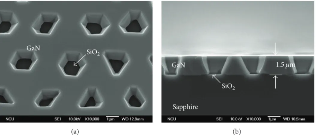
High-density plasma was used for SiO2etching.Figure 1(a)
shows the specification of the patterned SiO2 AlN/sapphire
template. The pitch and the diameter of the patterned SiO2
microdisk were 3.4 and 2𝜇m. Figure 1(b) shows the tilted
view of the scanning electron microscope (SEM) image of the
patterned SiO2AlN/sapphire template.
In this study we controlled void shapes by IFELOG com-prising three growth steps, with each step having a specific function. The first step (Step 1) involved the initial formation of GaN seeds exposed on PVD AlN buffer layer. The second step (Step 2) involved the growth performed only against the c-plane growth, and the final step (Step 3) involved the
coalescence. Trimethylgallium (TMGa) and ammonia (NH3)
were, respectively, used as gallium and nitrogen sources during growth. The GaN epitaxial layer grown on a patterned
SiO2AlN/sapphire template with rectangular, triangular, and
pillar voids was labeled as sample-R, sample-T, and sample-P, respectively.
At the onset of GaN growth, the growth temperature and
chamber pressure in Step 1 were set at 1050∘C and 400 torr.
The growth times of sample-R, sample-T, and sample-P in the same step were 1500, 750, and 1500 s, respectively. The growth
temperature and chamber pressure in Step 2 were 1050∘C and
100 torr. Pulsed growth technique was applied to obtain c-plane growth in this step, which is generally used to grow GaN
nanorod arrays [32]. Hence, this technique enhances the
c-plane growth direction. The respective pulsed growth periods of sample-R, sample-T, and sample-P were 60, 60, and 360,
respectively. The flow rates of TMGa and NH3were 17 sccm
and 3.5 slm; the injection times of TMGa and NH3were 3 and
5 s. Following the pulsed growth, Step 3 was performed with
growth temperature and chamber pressure set at 1080∘C and
400 torr. Conventional undoped-GaN with neither IFELOG
technology nor patterned SiO2 AlN/sapphire template was
prepared (i.e., sample-C) for comparative purposes.
The samples were examined by optical microscopy (OM), SEM, X-ray diffraction (XRD), atomic force microscopy (AFM), and transmission electron microscopy (TEM) to discuss the distribution of IFELOG in detail.
3. Results and Discussion
Figure 2 shows the cross-sectional SEM images of GaN epitaxial layers with differently shaped air voids utilizing
IFELOG on the same template.Figure 2(a)shows the
cross-sectional SEM images of sample-R with embedded rectan-gular air voids, each having a width and height of 1.00 and
1.00 𝜇m 0.10 𝜇m (a) 0.50 𝜇m 0.60 𝜇m (b) 1.12 𝜇m 0.55 𝜇m (c)
Figure 2: Cross-sectional SEM images of (a) sample-R, (b) sample-T, and (c) sample-P.
0.10𝜇m.Figure 2(b)shows the cross-sectional SEM images of sample-T with embedded triangular air voids, each having a
width and height of 0.60 and 0.50𝜇m; the angle of inclination
of the voids was 54∘. Figure 2(c)shows the cross-sectional
SEM images of sample-P with embedded pillar-shaped air
voids, each having a width and height of 0.55 and 1.12𝜇m.
Figure 3(a) shows the growth model of the GaN epitaxial layer with various air voids. At the onset of IFELOG, we obtained different distances between GaN seeds by adjusting
the growth time in Step 1 (Figures 3(a-2) and3(b-2)). We
also controlled the void heights by changing the pulsed
growth periods in Step 2 (Figures3(a-3) and3(c-3)).Figure 4
shows the tilted and cross-sectional SEM images of the GaN epitaxial layers of sample-R after Step-2 growth in the IFELOG technology. The standing GaN seeds confirmed that this technique induced c-plane growth. We also found that the GaN seeds were not able to deposit the entire AlN area during Step-1 growth, which will be discussed in more
detail inFigure 7. Considering that the samples had different
growth time combinations in between steps, we obtained the various diameters and heights of GaN seeds. Ali etal. reported that the diameter of hexagonal holes between GaN affects
void shape control [25]. In other words, the distances between
GaN seeds define the void shape after coalescence. Figures
3(a-4),3(b-4), and3(c-4) show the coalesced growth in Step-3
growth. Narrowing the gap inhibits the source gas molecules from diffusing to the bottom, which eventually forms the
Table 1: Full width at half-maximum values of𝜔 rocking curves measured by XRD. Sample FWHM (arcsecs) (002) (004) (006) (102) (105) Sample-C 485 479 480 600 603 Sample-R 376 362 355 322 384 Sample-T 433 454 420 408 459 Sample-P 416 420 409 360 426
embedded air voids that are responsible for the formation of differently shaped air voids (i.e., sample-R, sample-T, and
sample-P) [33].
The crystal quality of the GaN epitaxial layer was inves-tigated by XRD and AFM. Heying et al. reported the pure edge TD to be insensitive to the symmetric (0 0 l) rocking
curves with𝑙 nonzero and to distort only the (ℎ 𝑘 𝑙) planes
with either ℎ or 𝑘 nonzero. In other words, the decrease
in the FWHM values is regarded as a reduction in TDs [34–36].Table 1shows the respective values of full width at half maximum (FWHM) of the GaN (0 0 2) peak, GaN (0 0 4) peak, GaN (0 0 6) peak, GaN (1 0 2) peak, and GaN (1 0 5) peak for sample-C, sample-R, sample-T, and sample-P, respectively. All of the XRD results showed an improvement in IFELOG, particularly for sample-R, which
AlN Template (a-1) (a-2) (a-3) (a-4) (a-5) (b-1) (b-2) (b-3) (b-4) (b-5) (c-1) (c-2) (c-3) (c-4) (c-5)
(a) sample-R (b) sample-T (c) sample-P
Step-1 growth Step-2 growth Step-3 growth Sapphire GaN Rectangular air void AlN Sapphire GaN Triangular air void AlN Sapphire GaN Pillar-shaped air void
SiO2 SiO2 SiO2
Figure 3: The proposed growth model of (a) sample-R, (b) sample-T, and (c) sample-P.
GaN SiO2 (a) GaN Sapphire SiO2 1.5 𝜇m (b)
Figure 4: (a) Tilted and (b) cross-sectional SEM images of the sample-R GaN epitaxial layers after Step-1 and Step-2 growth in the IFELOG technology.
0 2.50 5.00 0 2.50 5.00 (𝜇m) 15.0 7.5 0.0 (nm) (a) 0 2.50 5.00 0 2.50 5.00 (𝜇m) 15.0 7.5 0.0 (nm) (b) 0 2.50 5.00 0 2.50 5.00 (𝜇m) 15.0 7.5 0.0 (nm) (c) 0 2.50 5.00 15.0 7.5 0.0 (nm) 0 2.50 5.00 (𝜇m) (d)
Figure 5: The EPD images over 5× 5 𝜇m2scanning area of (a) sample-C, (b) sample-R, (c) sample-T, and (d) sample-P.
reduced the GaN (1 0 2) from 600 arcsec to 322 arcsec. XRD data showed that IFELOG significantly enhanced the crystal quality due to the lateral growth beside the embedded air voids. The bending dislocations were observed in the TEM images.
A wet etching experiment was conducted in H3PO4
solu-tion at 250∘C to determine the etching pit densities (EPDs)
for GaN samples, and the samples were then examined using AFM. After wet etching, numerous hexagonal etching pits were observed on the surface. These etching pits were produced by the threading dislocations propagating to the surface of GaN, which originate from the interface between
GaN and substrate.Figure 5shows the EPD images over a
5 × 5 𝜇m2 scanning area of C, R,
T, and P. The EPDs of C, R,
sample-T, and sample-P were 5.3 × 10⁸, 2.4 × 10⁸, 2.7 × 10⁸, and
2.2× 10⁸/cm2, respectively. These results indicated that the
dislocation densities could be reduced in GaN epilayer using
IFELOG technology, which also corresponded to the XRD result.
TEM was used to analyze the reduction in the dislocation
density. Figure 6 shows the TEM images of the GaN
epi-taxial layer overgrown on the patterned SiO2 AlN/sapphire
template. The bended TDs were led by the coalesced growth
beside the voids [26], which eventually developed into
stacking faults (inset of Figure 6(c). Recent studies have
reported that TDs can be blocked by SiO2and stacking faults
mentioned above [37, 38]. Based on the TEM images, the
decrease in FWHM of the GaN peak and EPDs was caused by the significant decrease in TDs of the GaN epitaxial layer through IFELOG.
Figures7(a),7(b), and7(c)show the OM images of
sam-ple-R, sample-T, and sample-P, respectively. The OM images
show that the patterned SiO2 microdisk was surrounded
by expanded voids. Among all the samples, sample-R and sample-T had the most and least numbers of expanded
GaN Void Sapphire 1 𝜇m SiO2 (a) GaN Sapphire Void SiO2 1 𝜇m (b) GaN Void Sapphire SiO2 1 𝜇m 200 nm (c)
Figure 6: The TEM images of (a) sample-R, (b) sample-T, and (c) sample-P.
(a) (b)
(c)
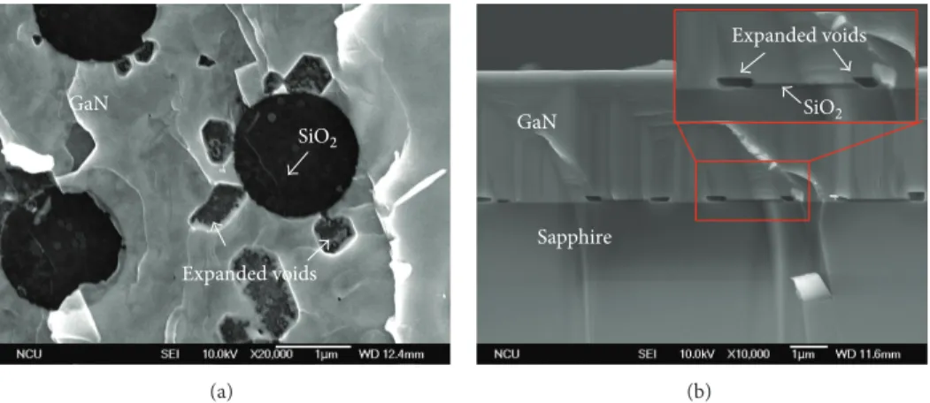
GaN Expanded voids SiO2 (a) Expanded voids GaN Sapphire SiO2 (b)
Figure 8: (a) The SEM image of sample-R lifted off by diamond cutter. (b) The cross-sectional SEM image of sample-R.
voids. Lift-off template surface and cross-section SEM mea-surements were performed to further clarify the cause of
the expanded voids that surrounded the patterned SiO2
microdisk. Sample-R was lifted off by a diamond cutter and it was found that the expanded voids surrounded the
patterned SiO2 microdisk (Figure 8(a)).Figure 8(b) shows
the cross-sectional SEM images prepared to clearly observe
the interface between SiO2and the GaN epitaxial layer. The
formation of expanded voids was caused by the discontinuous island-type growth characteristic of the GaN seed layer in the beginning. In other words, GaN seeds were not able to deposit the entire AlN area during Step-1 growth, which resulted in
residual vacancies beside the patterned SiO2microdisk. These
vacancies were converted into expanded voids, which had the similar function with the voids generated from the nanorod
template [23]. Such behavior can increase the lateral growth
and lower the TDs. These expanded voids were suggested to have positive effects on the quality of the GaN epitaxial layer because of the enhancement in XRD data and EPD result of sample-R, which had the most number of expanded voids.
4. Conclusion
We successfully demonstrated an interruption-free epitaxial lateral overgrowth technology by combining sputter AlN buffer layer and pulsed growth method. By adjusting Step-1 growth time and the periods of Step-2 growth, we easily controlled the void shape by the same template. The growth model was proposed to explain the formation of differently shaped air voids based on the SEM results. AFM images show that the epitaxial layer grown by IFELOG technology has lower etching pit densities, thereby increasing the volume of defect-free regions and bending TDs. XRD data suggests that we can decrease the FWHM of the GaN (0 0 2) and (1 0 2) peaks from 485 arcsec to 376 arcsec and from 600 arcsec to 322 arcsec in sample-R. IFELOG technology not only simplified the fabrication of templates, but also greatly enhanced the quality of the GaN epitaxial layer and yielded an uninterrupted growth.
Conflict of Interests
The authors declare that there is no conflict of interests regarding the publication of this paper.
Acknowledgment
The authors would like to acknowledge the financial support from National Science Council of Taiwan for their research Grants of NSC 101-2221-E-009-028-MY3 and NSC-3113-P-009-007-CC2.
References
[1] T. Mukai, M. Yamada, and S. Nakamura, “Characteristics of InGaN-based UV/blue/green/amber/red light-emitting dio-des,” Japanese Journal of Applied Physics, Part 1: Regular Papers
and Short Notes and Review Papers, vol. 38, no. 7, pp. 3976–3981,
1999.
[2] Y. Narukawa, I. Niki, K. Izuno, M. Yamada, Y. Murazaki, and T. Mukai, “Phosphor-conversion white light emitting diode using InGaN near-ultraviolet chip,” Japanese Journal of Applied
Physics, Part 2: Letters, vol. 41, no. 4, pp. L371–L373, 2002.
[3] Y. P. Hsu, S. J. Chang, Y. K. Su et al., “Lateral epitaxial patterned sapphire InGaN/GaN MQW LEDs,” Journal of Crystal Growth, vol. 261, no. 4, pp. 466–470, 2004.
[4] D. Kapolnek, S. Keller, R. Vetury et al., “Anisotropic epitaxial lateral growth in GaN selective area epitaxy,” Applied Physics
Letters, vol. 71, no. 9, pp. 1204–1206, 1997.
[5] T. S. Zheleva, O.-H. Nam, M. D. Bremser, and R. F. Davis, “Dislocation density reduction via lateral epitaxy in selectively grown GaN structures,” Applied Physics Letters, vol. 71, no. 17, pp. 2472–2474, 1997.
[6] M. Hansen, P. Fini, M. Craven, B. Heying, J. S. Speck, and S. P. DenBaars, “Morphological and optical properties of InGaN laser diodes on laterally overgrown GaN,” Journal of Crystal
Growth, vol. 234, no. 4, pp. 623–630, 2002.
[7] I.-H. Kim, C. Sone, O.-H. Nam, Y.-J. Park, and T. Kim, “Crystal tilting in GaN grown by pendoepitaxy method on sapphire substrate,” Applied Physics Letters, vol. 75, no. 26, pp. 4109–4111, 1999.
R. F. Davis, “Investigations regarding the maskless Pendeo-epitaxial growth of GaN films prior to coalescence,” IEEE
Jour-nal of Quantum Electronics, vol. 38, no. 8, pp. 1006–1016, 2002.
[9] C. I. H. Ashby, C. C. Mitchell, J. Han et al., “Low-dislocation-density GaN from a single growth on a textured substrate,”
Applied Physics Letters, vol. 77, no. 20, pp. 3233–3235, 2000.
[10] H. Miyake, R. Takeuchi, K. Hiramatsu et al., “High quality GaN grown by facet-controlled ELO, (FACELO) technique,” Physica
Status Solidi (A), vol. 194, pp. 545–549, 2002.
[11] K. Hiramatsu, K. Nishiyama, M. Onishi et al., “Fabrication and characterization of low defect density GaN using facet-controlled epitaxial lateral overgrowth (FACELO),” Journal of
Crystal Growth, vol. 221, no. 1–4, pp. 316–326, 2000.
[12] Y.-B. Lee, T. Wang, Y.-H. Liu et al., “High-performance 348 nm AlGaN/GaN-based ultraviolet-light-emitting diode with a SiN buffer layer,” Japanese Journal of Applied Physics, Part 1: Regular
Papers and Short Notes and Review Papers, vol. 41, no. 7, pp.
4450–4453, 2002.
[13] Y.-K. Ee, J. M. Biser, W. Cao, H. M. Chan, R. P. Vinci, and N. Tansu, “Metalorganic vapor phase epitaxy of III-nitride light-emitting diodes on nanopatterned AGOG sapphire substrate by abbreviated growth mode,” IEEE Journal on Selected Topics in
Quantum Electronics, vol. 15, no. 4, pp. 1066–1072, 2009.
[14] Y.-K. Ee, X.-H. Li, J. Biser et al., “Abbreviated MOVPE nucle-ation of III-nitride light-emitting diodes on nano-patterned sapphire,” Journal of Crystal Growth, vol. 312, no. 8, pp. 1311–1315, 2010.
[15] W. Cao, J. M. Biser, Y.-K. Ee et al., “Dislocation structure of GaN films grown on planar and nano-patterned sapphire,” Journal of
Applied Physics, vol. 110, no. 5, Article ID 053505, 2011.
[16] G. Martinez-Criado, M. Kuball, M. Benyoucef et al., “Free-standing GaN grown on epitaxial lateral overgrown GaN substrates,” Journal of Crystal Growth, vol. 255, no. 3-4, pp. 277– 281, 2003.
[17] C.-F. Lin, J.-J. Dai, M.-S. Lin et al., “An AlN sacrificial buffer layer inserted into the GaN/patterned sapphire substrate for a chemical lift-off process,” Applied Physics Express, vol. 3, no. 3, Article ID 031001, 2010.
[18] S. Bohyama, H. Miyake, K. Hiramatsu, Y. Tsuchida, and T. Maeda, “Freestanding GaN substrate by advanced facet-con-trolled epitaxial lateral overgrowth technique with masking side facets,” Japanese Journal of Applied Physics, Part 2: Letters, vol. 44, no. 1–7, pp. L24–L26, 2005.
[19] W.-K. Wang, D.-S. Wuu, W.-C. Shih et al., “Near-ultraviolet InGaN/GaN light-emitting diodes grown on patterned sapphire substrates,” Japanese Journal of Applied Physics, Part 1: Regular
Papers and Short Notes and Review Papers, vol. 44, no. 4, pp.
2512–2515, 2005.
[20] W.-C. Lai, Y.-Y. Yang, L.-C. Peng, S.-W. Yang, Y.-R. Lin, and J.-K. Sheu, “GaN-based light emitting diodes with embedded SiO2 pillars and air gap array structures,” Applied Physics Letters, vol. 97, no. 8, Article ID 081103, 2010.
[21] M. Ali, O. Svensk, L. Riuttanen et al., “Enhancement of near-UV GaN LED light extraction efficiency by GaN/sapphire template patterning,” Semiconductor Science and Technology, vol. 27, no. 8, Article ID 082002, 2012.
[22] S. D. Hersee, X. Y. Sun, X. Wang, M. N. Fairchild, J. Liang, and J. Xu, “Nanoheteroepitaxial growth of GaN on Si nanopillar arrays,” Journal of Applied Physics, vol. 97, no. 12, Article ID 124308, 2005.
improvement of near-ultraviolet nitride-based light-emitting-diode prepared on GaN nano-rod arrays by metalorganic chem-ical vapor deposition,” IEEE Journal of Quantum Electronics, vol. 50, no. 3, article 129, 2014.
[24] Z. Liliental-Weber, X. Ni, and H. Morkoc, “Structural perfection of laterally overgrown GaN layers grown in polar- and non-polar directions,” Journal of Materials Science: Materials in
Electronics, vol. 19, no. 8-9, pp. 815–820, 2008.
[25] M. Ali, A. E. Romanov, S. Suihkonen et al., “Void shape control in GaN re-grown on hexagonally patterned mask-less GaN,”
Journal of Crystal Growth, vol. 315, no. 1, pp. 188–191, 2011.
[26] M. Ali, A. E. Romanov, S. Suihkonen et al., “Analysis of threading dislocations in void shape controlled GaN re-grown on hexagonally patterned mask-less GaN,” Journal of Crystal
Growth, vol. 344, no. 1, pp. 59–64, 2012.
[27] J.-J. Dai, C.-F. Lin, G.-M. Wang, and M.-S. Lin, “Enhanced the light extraction efficiency of an InGaN light emitting diodes with an embedded rhombus-like air-void structure,” Applied
Physics Express, vol. 3, no. 7, Article ID 071002, 2010.
[28] C.-H. Yen, W.-C. Lai, Y.-Y. Yang et al., “GaN-based light-emitting diode with sputtered AlN nucleation layer,” IEEE
Photonics Technology Letters, vol. 24, no. 4, pp. 294–296, 2012.
[29] Y. H. Yeh, J. K. Sheu et al., “InGaN flip-chip light emitting diodes with embedded air voids as light-scattering layer,” IEEE Electron
Device Letters, vol. 34, no. 12, pp. 1542–1544, 2013.
[30] J.-K. Sheu, Y.-H. Yeh, S.-J. Tu, M.-L. Lee, P. C. Chen, and W.-C. Lai, “Improved output power of GaN-based blue LEDs by forming air voids on Ar-implanted sapphire substrate,” Journal
of Lightwave Technology, vol. 31, no. 8, Article ID 6464504, pp.
1318–1322, 2013.
[31] J.-K. Sheu, S.-J. Tu, Y.-H. Yeh, M.-L. Lee, and W.-C. Lai, “Gal-lium nitride-based light-emitting diodes with embedded air voids grown on Ar-implanted AlN/sapphire substrate,” Applied
Physics Letters, vol. 101, no. 15, Article ID 151103, 2012.
[32] S. D. Hersee, X. Sun, and X. Wang, “The controlled growth of GaN nanowires,” Nano Letters, vol. 6, no. 8, pp. 1808–1811, 2006. [33] H. J. Oh, S. W. Rhee, and I. S. Kang, “Simulation of CVD process by boundary integral technique,” Journal of the Electrochemical
Society, vol. 139, no. 6, pp. 1714–1720, 1992.
[34] H. Heinke, V. Kirchner, S. Einfeldt, and D. Hommel, “X-ray diffraction analysis of the defect structure in epitaxial GaN,”
Applied Physics Letters, vol. 77, no. 14, pp. 2145–2147, 2000.
[35] Y. Iyechika, M. Shimizu, T. Maeda, H. Miyake, and K. Hira-matsu, “X-ray analysis of twist and tilt of GaN prepared by facet-controlled epitaxial lateral overgrowth (FACELO),” Japanese
Journal of Applied Physics, Part 2: Letters, vol. 42, no. 7, pp. L732–
L734, 2003.
[36] B. Heying, X. H. Wu, S. Keller et al., “Role of threading disloca-tion structure on the x-ray diffracdisloca-tion peak widths in epitaxial GaN films,” Applied Physics Letters, vol. 68, article 643, 1995. [37] C. H. Chiu, H. H. Yen, C. L. Chao et al., “Nanoscale epitaxial
lateral overgrowth of GaN-based light-emitting diodes on a SiO2 nanorod-array patterned sapphire template,” Applied
Physics Letters, vol. 93, no. 8, Article ID 081108, 2008.
[38] D. S. Wuu, W. K. Wang, K. S. Wen et al., “Fabrication of pyra-midal patterned sapphire substrates for high-efficiency InGaN-based light emitting diodes,” Journal of the Electrochemical
Society, vol. 153, no. 8, Article ID 063608JES, pp. G765–G770,
Submit your manuscripts at
http://www.hindawi.com
Hindawi Publishing Corporation
http://www.hindawi.com Volume 2014
Inorganic Chemistry
International Journal of
Hindawi Publishing Corporation
http://www.hindawi.com Volume 2014
Photoenergy
Hindawi Publishing Corporation
http://www.hindawi.com Volume 2014
Carbohydrate
Chemistry
International Journal ofHindawi Publishing Corporation
http://www.hindawi.com Volume 2014
Journal of
Chemistry
Hindawi Publishing Corporation
http://www.hindawi.com Volume 2014
Physical Chemistry
Hindawi Publishing Corporation http://www.hindawi.com Analytical Methods in Chemistry Journal of Volume 2014 Bioinorganic Chemistry and Applications Hindawi Publishing Corporation
http://www.hindawi.com Volume 2014
Spectroscopy
International Journal ofHindawi Publishing Corporation
http://www.hindawi.com Volume 2014
The Scientific
World Journal
Hindawi Publishing Corporation
http://www.hindawi.com Volume 2014
Medicinal Chemistry
Hindawi Publishing Corporation
http://www.hindawi.com Volume 2014
Chromatography Research International
Hindawi Publishing Corporation
http://www.hindawi.com Volume 2014
Applied ChemistryJournal of
Hindawi Publishing Corporation
http://www.hindawi.com Volume 2014
Hindawi Publishing Corporation
http://www.hindawi.com Volume 2014 Theoretical Chemistry Journal of
Hindawi Publishing Corporation
http://www.hindawi.com Volume 2014
Journal of
Spectroscopy
Analytical Chemistry
Hindawi Publishing Corporation
http://www.hindawi.com Volume 2014
Journal of
Hindawi Publishing Corporation
http://www.hindawi.com Volume 2014 Quantum Chemistry
Hindawi Publishing Corporation
http://www.hindawi.com Volume 2014
International
Electrochemistry
International Journal of Hindawi Publishing Corporationhttp://www.hindawi.com Volume 2014
Hindawi Publishing Corporation
http://www.hindawi.com Volume 2014